TLC555
LinCMOS TIMER
SLFS043F - SEPTEMBER 1983 - REVISED FEBRUARY 2005
1
POST OFFICE BOX 655303
∑
DALLAS, TEXAS 75265
D
Very Low Power Consumption
- 1 mW Typ at V
DD
= 5 V
D
Capable of Operation in Astable Mode
D
CMOS Output Capable of Swinging Rail
to Rail
D
High Output-Current Capability
- Sink 100 mA Typ
- Source 10 mA Typ
D
Output Fully Compatible With CMOS, TTL,
and MOS
D
Low Supply Current Reduces Spikes
During Output Transitions
D
Single-Supply Operation From 2 V to 15 V
D
Functionally Interchangeable With the
NE555; Has Same Pinout
D
ESD Protection Exceeds 2000 V Per
MIL-STD-883C, Method 3015.2
D
Available in Q-Temp Automotive
High Reliability Automotive Applications
Configuration Control/Print Support
Qualification to Automotive Standards
description
The TLC555 is a monolithic timing circuit
fabricated using the TI LinCMOS
process. The
timer is fully compatible with CMOS, TTL, and
MOS logic and operates at frequencies up to
2 MHz. Because of its high input impedance, this
device uses smaller timing capacitors than those
used by the NE555. As a result, more accurate
time delays and oscillations are possible. Power
consumption is low across the full range of power
supply voltage.
Like the NE555, the TLC555 has a trigger level equal to approximately one-third of the supply voltage and a
threshold level equal to approximately two-thirds of the supply voltage. These levels can be altered by use of
the control voltage terminal (CONT). When the trigger input (TRIG) falls below the trigger level, the flip-flop is
set and the output goes high. If TRIG is above the trigger level and the threshold input (THRES) is above the
threshold level, the flip-flop is reset and the output is low. The reset input (RESET) can override all other inputs
and can be used to initiate a new timing cycle. If RESET is low, the flip-flop is reset and the output is low.
Whenever the output is low, a low-impedance path is provided between the discharge terminal (DISCH) and
GND. All unused inputs should be tied to an appropriate logic level to prevent false triggering.
While the CMOS output is capable of sinking over 100 mA and sourcing over 10 mA, the TLC555 exhibits greatly
reduced supply-current spikes during output transitions. This minimizes the need for the large decoupling
capacitors required by the NE555.
Please be aware that an important notice concerning availability, standard warranty, and use in critical applications of
Texas Instruments semiconductor products and disclaimers thereto appears at the end of this data sheet.
Copyright
1983-2005, Texas Instruments Incorporated
PRODUCTION DATA information is current as of publication date.
Products conform to specifications per the terms of Texas Instruments
standard warranty. Production processing does not necessarily include
testing of all parameters.
LinCMOS is a trademark of Texas Instruments.
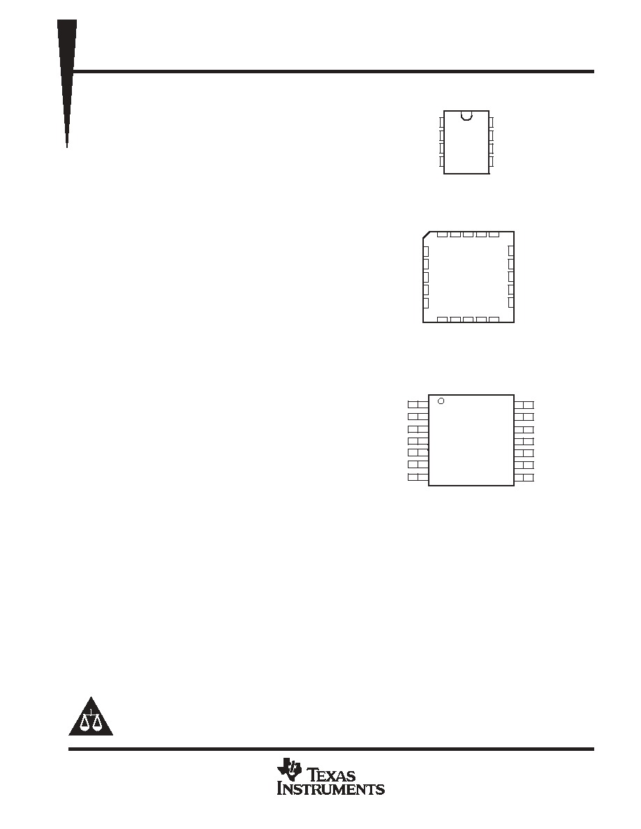
3
2
1 20 19
9 10 11 12 13
4
5
6
7
8
18
17
16
15
14
NC
DISCH
NC
THRES
NC
NC
TRIG
NC
OUT
NC
FK PACKAGE
(TOP VIEW)
NC
GND
NC
CONT
NC
V
NC
RESET
NC
NC
DD
D, DB, JG, OR P PACKAGE
(TOP VIEW)
1
2
3
4
8
7
6
5
GND
TRIG
OUT
RESET
V
DD
DISCH
THRES
CONT
NC - No internal connection
1
2
3
4
5
6
7
14
13
12
11
10
9
8
GND
NC
TRIG
NC
OUT
NC
RESET
V
DD
NC
DISCH
NC
THRES
NC
CONT
PW PACKAGE
(TOP VIEW)
On products compliant to MIL PRF 38535, all parameters are tested
unless otherwise noted. On all other products, production
processing does not necessarily include testing of all parameters.

TLC555
LinCMOS TIMER
SLFS043F - SEPTEMBER 1983 - REVISED FEBRUARY 2005
2
POST OFFICE BOX 655303
∑
DALLAS, TEXAS 75265
description (continued)
The TLC555C is characterized for operation from 0
∞
C to 70
∞
C. The TLC555I is characterized for operation from
-40
∞
C to 85
∞
C. The TLC555Q is characterized for operation over the automotive temperature range of -40
∞
C
to 125
∞
C. The TLC555M is characterized for operation over the full military temperature range of -55
∞
C to
125
∞
C.
AVAILABLE OPTIONS
PACKAGED DEVICES
TA
VDD
RANGE
SMALL
OUTLINE
(D)
SSOP
(DB)
CHIP CARRIER
(FK)
CERAMIC DIP
(JG)
PLASTIC DIP
(P)
TSSOP
(PW)
0
∞
C to 70
∞
C
2 V to 15 V
TLC555CD
TLC555CDB
--
--
TLC555CP
TLC555CPW
-40
∞
C to 85
∞
C
3 V to 15 V
TLC555ID
--
--
--
TLC555IP
--
-40
∞
C to 125
∞
C
5 V to 15 V
TLC555QD
--
--
--
--
--
-55
∞
C to 125
∞
C
5 V to 15 V
TLC555MD
--
TLC555MFK
TLC555MJG
TLC555MP
--
For the most current package and ordering information, see the Package Option Addendum at the end of this document, or see the TI web site
at www.ti.com.
This package is available taped and reeled. Add the R suffix to device type (e.g., TLC555CDR).
FUNCTION TABLE
RESET VOLTAGE
TRIGGER VOLTAGE
THRESHOLD VOLTAGE
OUTPUT
DISCHARGE SWITCH
<MIN
Irrelevant
Irrelevant
L
On
>MAX
<MIN
Irrelevant
H
Off
>MAX
>MAX
>MAX
L
On
>MAX
>MAX
<MIN
As previously established
For conditions shown as MIN or MAX, use the appropriate value specified under electrical characteristics.
functional block diagram
GND
RESET
CONT
VDD
1
THRES
TRIG
R
R
R
DISCH
OUT
S
R
R1
Pin numbers are for all packages except the FK package. RESET can override TRIG, which can override THRES.
5
6
2
1
7
3
4
8

TLC555
TIMER
LinCMOS
SLFS043F - SEPTEMBER 1983 - REVISED FEBRUARY 2005
POST OFFICE BOX 655303 DALLAS, TEXAS 75265
∑
3
equivalent
schematic (each channel)
THRES
CONT
TRIG
RESET
V
DD
DISCH
OUT
GND
T
ransistors
COMPONENT COUNT
Resistors
39
5

TLC555
LinCMOS TIMER
SLFS043F - SEPTEMBER 1983 - REVISED FEBRUARY 2005
4
POST OFFICE BOX 655303
∑
DALLAS, TEXAS 75265
absolute maximum ratings over operating free-air temperature range (unless otherwise noted)
Supply voltage, V
DD
(see Note 1)
18 V
. . . . . . . . . . . . . . . . . . . . . . . . . . . . . . . . . . . . . . . . . . . . . . . . . . . . . . . . . . . .
Input voltage range, V
I
(any input)
-0.3 to V
DD
. . . . . . . . . . . . . . . . . . . . . . . . . . . . . . . . . . . . . . . . . . . . . . . . . . . . .
Sink current, discharge or output
150 mA
. . . . . . . . . . . . . . . . . . . . . . . . . . . . . . . . . . . . . . . . . . . . . . . . . . . . . . . . . .
Source current, output, I
O
15 mA
. . . . . . . . . . . . . . . . . . . . . . . . . . . . . . . . . . . . . . . . . . . . . . . . . . . . . . . . . . . . . . . . .
Continuous total power dissipation
See Dissipation Rating Table
. . . . . . . . . . . . . . . . . . . . . . . . . . . . . . . . . . . . .
Operating free-air temperature range, T
A
: C-suffix 0
∞
C to 70
∞
C
. . . . . . . . . . . . . . . . . . . . . . . . . . . . . . . . . . . . . .
I-suffix -40
∞
C to 85
∞
C
. . . . . . . . . . . . . . . . . . . . . . . . . . . . . . . . . . . .
Q-suffix -40
∞
C to 125
∞
C
. . . . . . . . . . . . . . . . . . . . . . . . . . . . . . . . . .
M-suffix -55
∞
C to 125
∞
C
. . . . . . . . . . . . . . . . . . . . . . . . . . . . . . . . . .
Storage temperature range
-65
∞
C to 150
∞
C
. . . . . . . . . . . . . . . . . . . . . . . . . . . . . . . . . . . . . . . . . . . . . . . . . . . . . . . .
Case temperature for 60 seconds: FK package
260
∞
C
. . . . . . . . . . . . . . . . . . . . . . . . . . . . . . . . . . . . . . . . . . . . . .
Lead temperature 1,6 mm (1/16 inch) from case for 60 seconds: JG package
300
∞
C
. . . . . . . . . . . . . . . . . . . .
Lead temperature 1,6 mm (1/16 inch) from case for 10 seconds: D, DB, P, or PW package
260
∞
C
. . . . . . . .
Stresses beyond those listed under "absolute maximum ratings" may cause permanent damage to the device. These are stress ratings only and
functional operation of the device at these or any other conditions beyond those indicated under "recommended operating conditions" is not
implied. Exposure to absolute-maximum-rated conditions for extended periods may affect device reliability.
NOTE 1: All voltage values are with respect to network GND.
DISSIPATION RATING TABLE
PACKAGE
TA
25
∞
C
POWER RATING
DERATING FACTOR
ABOVE TA = 25
∞
C
TA = 70
∞
C
POWER RATING
TA = 85
∞
C
POWER RATING
TA = 125
∞
C
POWER RATING
D
DB
FK
JG
P
PW
725 mW
525 mW
1375 mW
1050 mW
1000 mW
525 mW
5.8 mW/
∞
C
4.2 mW/
∞
C
11.0 mW/
∞
C
8.4 mW/
∞
C
8.0 mW/
∞
C
4.2 mW/
∞
C
464 mW
336 mW
880 mW
672 mW
640 mW
336 mW
377 mW
273 mW
715 mW
546 mW
520 mW
273 mW
145 mW
105 mW
275 mW
210 mW
200 mW
105 mW
recommended operating conditions
MIN
MAX
UNIT
Supply voltage, VDD
2
15
V
TLC555C
0
70
Operating free-air temperature range, TA
TLC555I
-40
85
∞
C
Operating free-air temperature range, TA
TLC555Q
-40
125
∞
C
TLC555M
-55
125

TLC555
LinCMOS TIMER
SLFS043F - SEPTEMBER 1983 - REVISED FEBRUARY 2005
5
POST OFFICE BOX 655303
∑
DALLAS, TEXAS 75265
electrical characteristics at specified free-air temperature, V
DD
= 2 V for TLC555C, V
DD
= 3 V for
TLC555I
PARAMETER
TEST
TA
TLC555C
TLC555I
UNIT
PARAMETER
TEST
CONDITIONS
TA
MIN
TYP
MAX
MIN
TYP
MAX
UNIT
VIT
Threshold voltage
25
∞
C
0.95
1.33
1.65
1.6
2.4
V
VIT
Threshold voltage
Full range
0.85
1.75
1.5
2.5
V
IIT
Threshold current
25
∞
C
10
10
pA
IIT
Threshold current
MAX
75
150
pA
VI(TRIG)
Trigger voltage
25
∞
C
0.4
0.67
0.95
0.71
1
1.29
V
VI(TRIG)
Trigger voltage
Full range
0.3
1.05
0.61
1.39
V
II(TRIG)
Trigger current
25
∞
C
10
10
pA
II(TRIG)
Trigger current
MAX
75
150
pA
VI(RESET)
Reset voltage
25
∞
C
0.4
1.1
1.5
0.4
1.1
1.5
V
VI(RESET)
Reset voltage
Full range
0.3
2
0.3
1.8
V
II(RESET)
Reset current
25
∞
C
10
10
pA
II(RESET)
Reset current
MAX
75
150
pA
Control voltage (open circuit) as
a percentage of supply voltage
MAX
66.7%
66.7%
Discharge switch on-stage
IOL = 1 mA
25
∞
C
0.03
0.2
0.03
0.2
V
Discharge switch on-stage
voltage
IOL = 1 mA
Full range
0.25
0.375
V
Discharge switch off-stage
25
∞
C
0.1
0.1
nA
Discharge switch off-stage
current
MAX
0.5
120
nA
VOH
High-level output voltage
IOH = - 300 A
25
∞
C
1.5
1.9
2.5
2.85
V
VOH
High-level output voltage
IOH = - 300
µ
A
Full range
1.5
2.5
V
VOL
Low-level output voltage
IOL = 1 mA
25
∞
C
0.07
0.3
0.07
0.3
V
VOL
Low-level output voltage
IOL = 1 mA
Full range
0.35
0.4
V
IDD
Supply current
See Note 2
25
∞
C
250
250
µ
A
IDD
Supply current
See Note 2
Full range
400
500
µ
A
Full range is 0
∞
C to 70
∞
C for the TLC555C and -40
∞
C to 85
∞
C for the TLC555I. For conditions shown as MAX, use the appropriate value specified
in the recommended operating conditions table.
NOTE 2: These values apply for the expected operating configurations in which THRES is connected directly to DISCH or to TRIG.