
5
6
7
8
9
10
11
25
24
23
22
21
20
19
4
3
2
1 28
12 13 14 15 16
Q
B
Q
C
Q
D
NC
Q
E
Q
F
Q
G
B
C
D
NC
E
F
G
A
S1
S0
RCO
CLK
ENT
GND
NC
NC
ENP
Q
V
H
H
17 18
27 26
NC ≠ No internal connection
CC
S0
S1
A
B
C
D
E
F
G
H
ENT
GND
V
CC
ENP
Q
A
Q
B
Q
C
Q
D
Q
E
Q
F
Q
G
Q
H
CLK
RCO
1
2
3
4
5
6
7
8
9
10
11
12
24
23
22
21
20
19
18
17
16
15
14
13
SN54AS867, SN54AS869 . . . JT PACKAGE
SN74ALS867A, SN74ALS869, SN74AS867,
SN74AS869 . . . DW OR NT PACKAGE
(TOP VIEW)
SN54AS867, SN54AS869 . . . FK PACKAGE
(TOP VIEW)
A
Q
SN54AS867, SN54AS869
SN74ALS867A, SN74ALS869, SN74AS867, SN74AS869
SYNCHRONOUS 8-BIT UP/DOWN COUNTERS
SDAS115C ≠ DECEMBER 1982 ≠ REVISED JANUARY 1995
Copyright
©
1995, Texas Instruments Incorporated
1
POST OFFICE BOX 655303
∑
DALLAS, TEXAS 75265
∑
Fully Programmable With Synchronous
Counting and Loading
∑
SN74ALS867A and
AS867 Have
Asynchronous Clear; SN74ALS869 and
AS869 Have Synchronous Clear
∑
Fully Independent Clock Circuit
Simplifies Use
∑
Ripple-Carry Output for n-Bit Cascading
∑
Package Options Include Plastic
Small-Outline (DW) Packages, Ceramic
Chip Carriers (FK), and Standard Plastic
(NT) and Ceramic (JT) 300-mil DIPs
description
These synchronous, presettable, 8-bit up/down
counters feature internal-carry look-ahead
circuitry for cascading in high-speed counting
applications. Synchronous operation is provided
by having all flip-flops clocked simultaneously so
that the outputs change coincidentally with each
other when so instructed by the count-enable
(ENP, ENT) inputs and internal gating. This mode
of operation eliminates the output counting spikes
normally associated with asynchronous (ripple-
clock) counters. A buffered clock (CLK) input
triggers the eight flip-flops on the rising (positive-
going) edge of the clock waveform.
These counters are fully programmable; they may
be preset to any number between 0 and 255. The
load-input circuitry allows parallel loading of the
cascaded counters. Because loading is
synchronous, selecting the load mode disables
the counter and causes the outputs to agree with
the data inputs after the next clock pulse.
The carry look-ahead circuitry provides for cascading counters for n-bit synchronous applications without
additional gating. Two count-enable (ENP and ENT) inputs and a ripple-carry (RCO) output are instrumental
in accomplishing this function. Both ENP and ENT must be low to count. The direction of the count is determined
by the levels of the select (S0, S1) inputs as shown in the function table. ENT is fed forward to enable RCO. RCO
thus enabled produces a low-level pulse while the count is zero (all outputs low) counting down or 255 counting
up (all outputs high). This low-level overflow-carry pulse can be used to enable successive cascaded stages.
Transitions at ENP and ENT are allowed regardless of the level of CLK. All inputs are diode clamped to minimize
transmission-line effects, thereby simplifying system design.
These counters feature a fully independent clock circuit. With the exception of the asynchronous clear on the
SN74ALS867A and
AS867, changes at S0 and S1 that modify the operating mode have no effect on the Q
outputs until clocking occurs. For the
AS867 and
AS869, any time ENP and/or ENT is taken high, RCO either
goes or remains high. For the SN74ALS867A and SN74ALS869, any time ENT is taken high, RCO either goes
or remains high. The function of the counter (whether enabled, disabled, loading, or counting) is dictated solely
by the conditions meeting the stable setup and hold times.
PRODUCTION DATA information is current as of publication date.
Products conform to specifications per the terms of Texas Instruments
standard warranty. Production processing does not necessarily include
testing of all parameters.
SN54AS867, SN54AS869
SN74ALS867A, SN74ALS869, SN74AS867, SN74AS869
SYNCHRONOUS 8-BIT UP/DOWN COUNTERS
SDAS115C ≠ DECEMBER 1982 ≠ REVISED JANUARY 1995
2
POST OFFICE BOX 655303
∑
DALLAS, TEXAS 75265
description (continued)
The SN54AS867 and SN54AS869 are characterized for operation over the full military temperature range of
≠ 55
∞
C to 125
∞
C. The SN74ALS867A, SN74ALS869, SN74AS867, and SN74AS869 are characterized for
operation from 0
∞
C to 70
∞
C.
FUNCTION TABLE
S1
S0
FUNCTION
L
L
Clear
L
H
Count down
H
L
Load
H
H
Count up

SN54AS867, SN54AS869
SN74ALS867A, SN74ALS869, SN74AS867, SN74AS869
SYNCHRONOUS 8-BIT UP/DOWN COUNTERS
SDAS115C ≠ DECEMBER 1982 ≠ REVISED JANUARY 1995
3
POST OFFICE BOX 655303
∑
DALLAS, TEXAS 75265
logic symbols
ENT
ENP
CTRDIV 256
2,6D
3
A
4
B
5
C
6
D
22
21
20
19
0
1
S0
M
0
3
3,4CT=255
0R
7
E
8
F
9
G
10
H
18
17
16
15
1
2
S1
G4
11
G5
23
14
CLK
13
1,4CT=0
RCO
QA
QB
QC
QD
QE
QF
QG
QH
SN74ALS867A
ENT
ENP
CTRDIV 256
2,6D
3
A
4
B
5
C
6
D
22
21
20
19
0
1
S0
M
0
3
3,4CT=255
0,6R
7
E
8
F
9
G
10
H
18
17
16
15
1
2
S1
G4
11
G5
23
14
CLK
13
1,4CT=0
RCO
QA
QB
QC
QD
QE
QF
QG
QH
SN74ALS869
C6/1,4,5 ≠ /3,4,5 +
C6/1,4,5 ≠ /3,4,5 +
These symbols are in accordance with ANSI/IEEE Std 91-1984 and IEC Publication 617-12.
Pin numbers shown are for the DW, JT, and NT packages.

SN54AS867, SN54AS869
SN74ALS867A, SN74ALS869, SN74AS867, SN74AS869
SYNCHRONOUS 8-BIT UP/DOWN COUNTERS
SDAS115C ≠ DECEMBER 1982 ≠ REVISED JANUARY 1995
4
POST OFFICE BOX 655303
∑
DALLAS, TEXAS 75265
logic symbols (continued)
ENT
ENP
CTRDIV 256
2,6D
3
A
4
B
5
C
6
D
22
21
20
19
0
1
S0
M
0
3
3,4,5CT=255
0R
7
E
8
F
9
G
10
H
18
17
16
15
1
2
S1
G4
11
G5
23
14
CLK
13
1,4,5CT=0
RCO
QA
QB
QC
QD
QE
QF
QG
QH
AS867
ENT
ENP
CTRDIV 256
2,6D
3
A
4
B
5
C
6
D
22
21
20
19
0
1
S0
M
0
3
3,4,5CT=255
0,6R
7
E
8
F
9
G
10
H
18
17
16
15
1
2
S1
G4
11
G5
23
14
CLK
13
1,4,5CT=0
RCO
QA
QB
QC
QD
QE
QF
QG
QH
AS869
C6/1,4,5 ≠ /3,4,5 +
C6/1,4,5 ≠ /3,4,5 +
These symbols are in accordance with ANSI/IEEE Std 91-1984 and IEC Publication 617-12.
Pin numbers shown are for the DW, JT, and NT packages.
SN54AS867, SN54AS869
SN74ALS867A, SN74ALS869, SN74AS867, SN74AS869
SYNCHRONOUS 8-BIT UP/DOWN COUNTERS
SDAS115C ≠ DECEMBER 1982 ≠ REVISED JANUARY 1995
5
POST OFFICE BOX 655303
∑
DALLAS, TEXAS 75265
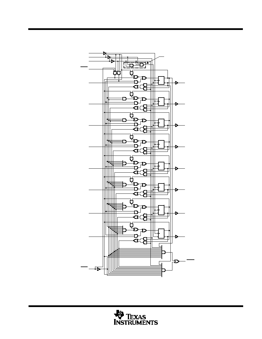
logic diagram (positive logic)
A
1D
R
C1
22
QA
14
1
2
23
3
B
1D
R
C1
21
QB
4
C
1D
R
C1
20
QC
5
D
1D
R
C1
19
QD
6
E
1D
R
C1
18
QE
7
ENP
S1
S0
CLK
F
1D
R
C1
17
QF
8
G
1D
R
C1
16
QG
9
H
1D
R
C1
15
QH
10
13
RCO
ENT
11
SN74ALS867A Only
(asynchronous clear)
SN74ALS867A, SN74ALS869
Pin numbers shown are for the DW, JT, and NT packages.
SN54AS867, SN54AS869
SN74ALS867A, SN74ALS869, SN74AS867, SN74AS869
SYNCHRONOUS 8-BIT UP/DOWN COUNTERS
SDAS115C ≠ DECEMBER 1982 ≠ REVISED JANUARY 1995
6
POST OFFICE BOX 655303
∑
DALLAS, TEXAS 75265
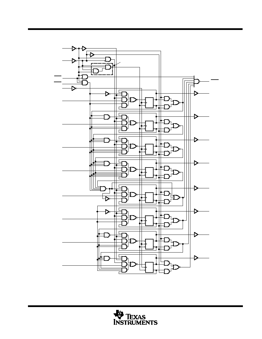
logic diagram (positive logic)
1D
R
C1
A
ENP
S1
S0
CLK
ENT
QA
RCO
1
2
11
23
14
3
13
22
1D
R
C1
B
QB
4
21
1D
R
C1
C
QC
5
20
1D
R
C1
D
QD
6
19
1D
R
C1
E
QE
7
18
AS867 Only
(asynchronous clear)
1D
R
C1
F
QF
8
17
1D
R
C1
G
QG
9
16
1D
R
C1
H
QH
10
15
AS867,
AS869
Pin numbers shown are for the DW, JT, and NT packages.
SN54AS867, SN54AS869
SN74ALS867A, SN74ALS869, SN74AS867, SN74AS869
SYNCHRONOUS 8-BIT UP/DOWN COUNTERS
SDAS115C ≠ DECEMBER 1982 ≠ REVISED JANUARY 1995
7
POST OFFICE BOX 655303
∑
DALLAS, TEXAS 75265
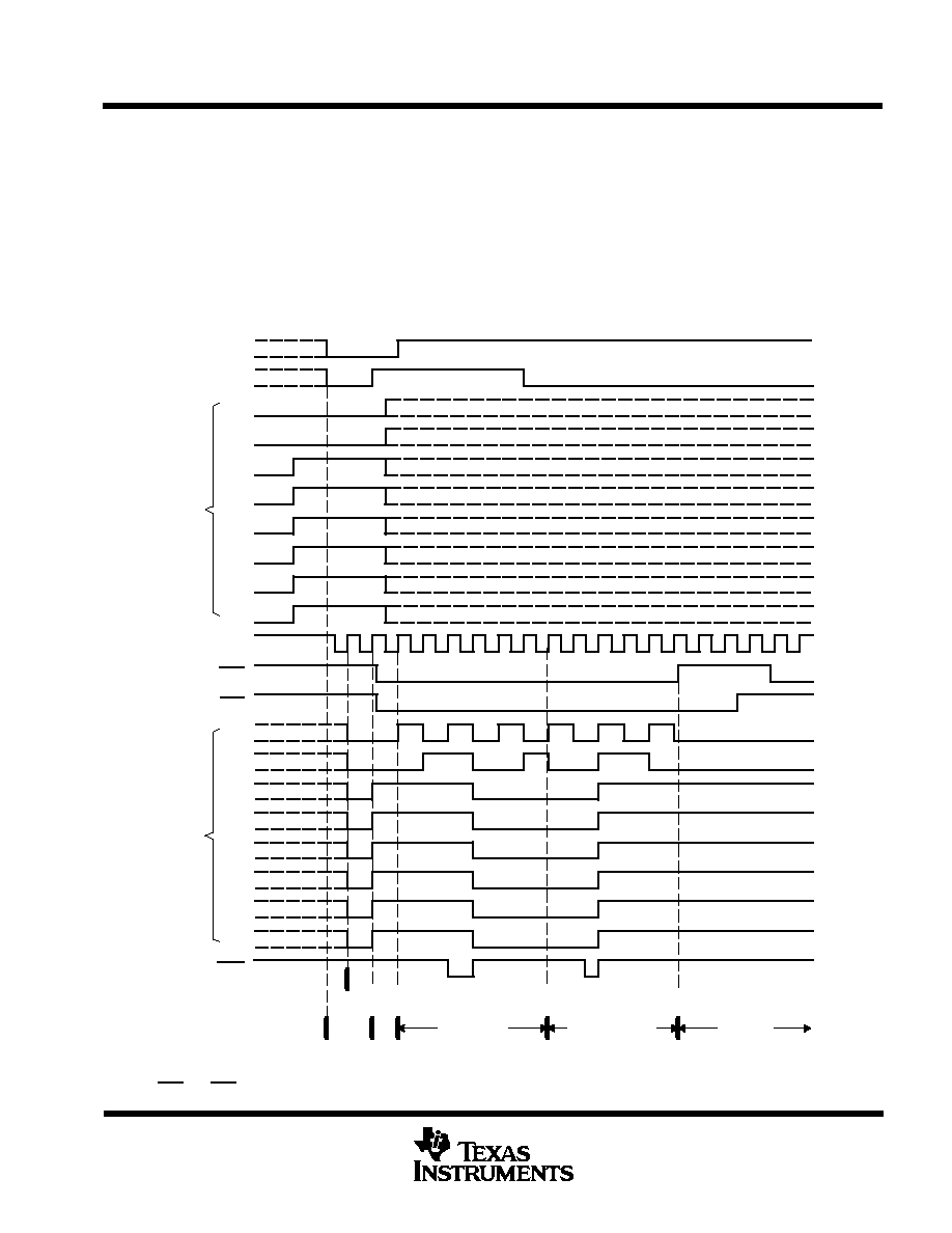
typical clear, preset, count, and inhibit sequences
The following sequence is illustrated below:
1.
Clear outputs to zero (SN74ALS867A and
AS867 are asynchronous;
SN74ALS869 and
AS869 are synchronous.)
2.
Preset to binary 252
3.
Count up to 253, 254, 255, 0, 1, and 2
4.
Count down to 1, 0, 255, 254, 253, and 252
5.
Inhibit
C
Async
Clear
D
E
F
CLK
ENP
ENT
QA
QB
QC
QD
RCO
Data
Inputs
Outputs
QE
QF
QG
QH
Count Down
G
H
B
A
S1
S0
Preset
Sync
Clear
252 253
255
254
255 254 253 252
0
1
2
1
0
Count Up
Inhibit
ENT and ENP both must be low for counting to occur.
SN54AS867, SN54AS869
SN74ALS867A, SN74ALS869, SN74AS867, SN74AS869
SYNCHRONOUS 8-BIT UP/DOWN COUNTERS
SDAS115C ≠ DECEMBER 1982 ≠ REVISED JANUARY 1995
8
POST OFFICE BOX 655303
∑
DALLAS, TEXAS 75265
absolute maximum ratings over operating free-air temperature range (unless otherwise noted)
Supply voltage, V
CC
7 V
. . . . . . . . . . . . . . . . . . . . . . . . . . . . . . . . . . . . . . . . . . . . . . . . . . . . . . . . . . . . . . . . . . . . . . . .
Input voltage, V
I
7 V
. . . . . . . . . . . . . . . . . . . . . . . . . . . . . . . . . . . . . . . . . . . . . . . . . . . . . . . . . . . . . . . . . . . . . . . . . . . .
Operating free-air temperature range, T
A
: SN74ALS867A
0
∞
C to 70
∞
C
. . . . . . . . . . . . . . . . . . . . . . . . . . . . . . . .
Storage temperature range
≠ 65
∞
C to 150
∞
C
. . . . . . . . . . . . . . . . . . . . . . . . . . . . . . . . . . . . . . . . . . . . . . . . . . . . . . .
Stresses beyond those listed under "absolute maximum ratings" may cause permanent damage to the device. These are stress ratings only, and
functional operation of the device at these or any other conditions beyond those indicated under "recommended operating conditions" is not
implied. Exposure to absolute-maximum-rated conditions for extended periods may affect device reliability.
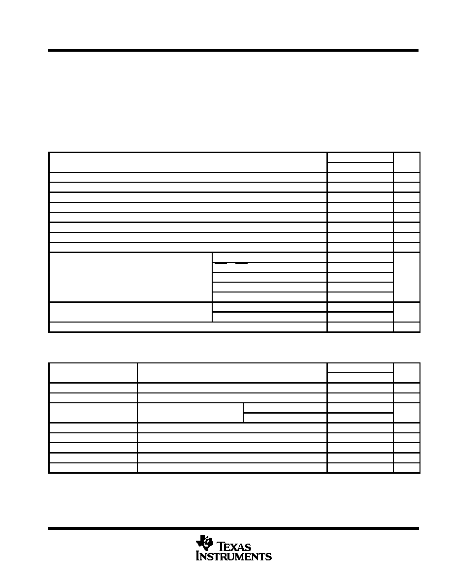
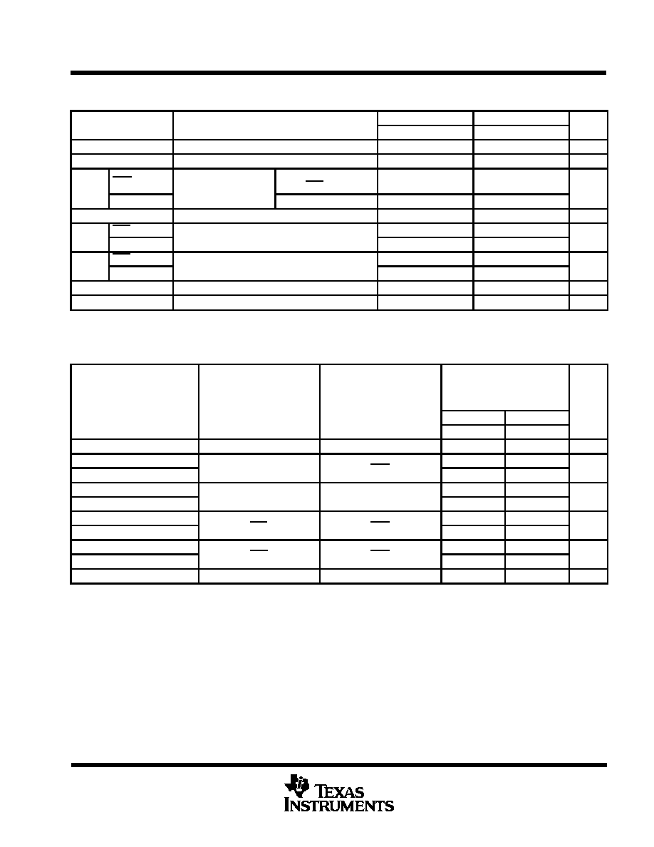
recommended operating conditions
SN74ALS867A
UNIT
MIN
NOM
MAX
UNIT
VCC
Supply voltage
4.5
5
5.5
V
VIH
High-level input voltage
2
V
VIL
Low-level input voltage
0.8
V
IOH
High-level output current
≠ 0.4
mA
IOL
Low-level output current
8
mA
fclock
Clock frequency
0
35
MHz
tw(clock)
Pulse duration, CLK high or low
14
ns
tw(clear)
Pulse duration of clear pulse, S0 and S1 low
10
ns
Data inputs A ≠ H
10
ENP or ENT
15
tsu
Setup time before CLK
S0 low and S1 high (load)
12
ns
S0 high and S1 low (count down)
12
S0 and S1 high (count up)
12
th
Hold time after CLK
S0 high after S1
or S1 high after S0
3
ns
th
Hold time after CLK
Data inputs A ≠ H
0
ns
TA
Operating free-air temperature
0
70
∞
C
electrical characteristics over recommended operating free-air temperature range (unless
otherwise noted)
PARAMETER
TEST CONDITIONS
SN74ALS867A
UNIT
PARAMETER
TEST CONDITIONS
MIN
TYP
MAX
UNIT
VIK
VCC = 4.5 V,
II = ≠18 mA
≠1.2
V
VOH
VCC = 4.5 V to 5.5 V,
IOH = ≠ 0.4 mA
VCC ≠ 2
V
VOL
VCC = 4 5 V
IOL = 4 mA
0.25
0.4
V
VOL
VCC = 4.5 V
IOL = 8 mA
0.35
0.5
V
II
VCC = 5.5 V,
VI = 7 V
0.1
mA
IIH
VCC = 5.5 V,
VI = 2.7 V
20
µ
A
IIL
VCC = 5.5 V,
VI = 0.4 V
≠ 0.2
mA
IOß
VCC = 5.5 V,
VO = 2.25 V
≠ 30
≠112
mA
ICC
VCC = 5.5 V
28
45
mA
All typical values are at VCC = 5 V, TA = 25
∞
C.
ß The output conditions have been chosen to produce a current that closely approximates one half of the true short-circuit output current, IOS.
SN54AS867, SN54AS869
SN74ALS867A, SN74ALS869, SN74AS867, SN74AS869
SYNCHRONOUS 8-BIT UP/DOWN COUNTERS
SDAS115C ≠ DECEMBER 1982 ≠ REVISED JANUARY 1995
9
POST OFFICE BOX 655303
∑
DALLAS, TEXAS 75265
switching characteristics (see Figure 1)
PARAMETER
FROM
(INPUT)
TO
(OUTPUT)
VCC = 4.5 V to 5.5 V,
CL = 50 pF,
RL = 500
,
TA = MIN to MAX
UNIT
(INPUT)
(OUTPUT)
SN74ALS867A
MIN
MAX
fmax
35
MHz
tPLH
CLK
RCO
4
14
ns
tPHL
CLK
RCO
4
14
ns
tPLH
CLK
Any Q
3
16
ns
tPHL
CLK
Any Q
3
16
ns
tPLH
ENT
RCO
3
14
ns
tPHL
ENT
RCO
2
9
ns
tPHL
S0 or S1 (clear mode)
Any Q
8
26
ns
tPLH
S0 or S1
RCO
4
16
ns
tPHL
(count up/down)
RCO
4
16
ns
tPLH
S0 or S1 (clear mode)
RCO
4
16
ns
For conditions shown as MIN or MAX, use the appropriate value specified under recommended operating conditions.
SN54AS867, SN54AS869
SN74ALS867A, SN74ALS869, SN74AS867, SN74AS869
SYNCHRONOUS 8-BIT UP/DOWN COUNTERS
SDAS115C ≠ DECEMBER 1982 ≠ REVISED JANUARY 1995
10
POST OFFICE BOX 655303
∑
DALLAS, TEXAS 75265
absolute maximum ratings over operating free-air temperature range (unless otherwise noted)
Supply voltage, V
CC
7 V
. . . . . . . . . . . . . . . . . . . . . . . . . . . . . . . . . . . . . . . . . . . . . . . . . . . . . . . . . . . . . . . . . . . . . . . .
Input voltage, V
I
7 V
. . . . . . . . . . . . . . . . . . . . . . . . . . . . . . . . . . . . . . . . . . . . . . . . . . . . . . . . . . . . . . . . . . . . . . . . . . . .
Operating free-air temperature range, T
A
: SN74ALS869
0
∞
C to 70
∞
C
. . . . . . . . . . . . . . . . . . . . . . . . . . . . . . . . .
Storage temperature range
≠ 65
∞
C to 150
∞
C
. . . . . . . . . . . . . . . . . . . . . . . . . . . . . . . . . . . . . . . . . . . . . . . . . . . . . . .
Stresses beyond those listed under "absolute maximum ratings" may cause permanent damage to the device. These are stress ratings only, and
functional operation of the device at these or any other conditions beyond those indicated under "recommended operating conditions" is not
implied. Exposure to absolute-maximum-rated conditions for extended periods may affect device reliability.
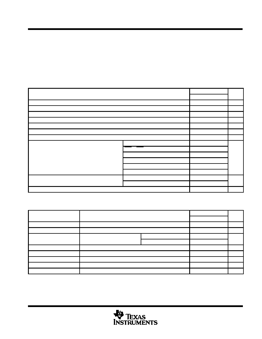
recommended operating conditions
SN74ALS869
UNIT
MIN
NOM
MAX
UNIT
VCC
Supply voltage
4.5
5
5.5
V
VIH
High-level input voltage
2
V
VIL
Low-level input voltage
0.8
V
IOH
High-level output current
≠ 0.4
mA
IOL
Low-level output current
8
mA
fclock
Clock frequency
0
35
MHz
tw(clock)
Pulse duration, CLK high or low
14
ns
Data inputs A ≠ H
10
ENP or ENT
15
t
Set p time before CLK
S0 and S1 low (clear)
13
ns
tsu
Setup time before CLK
S0 low and S1 high (load)
13
ns
S0 high and S1 low (count down)
13
S0 and S1 high (count up)
13
th
Hold time after CLK
S0 high after S1
or S1 high after S0
3
ns
th
Hold time after CLK
Data inputs A ≠ H
0
ns
TA
Operating free-air temperature
0
70
∞
C
electrical characteristics over recommended operating free-air temperature range (unless
otherwise noted)
PARAMETER
TEST CONDITIONS
SN74ALS869
UNIT
PARAMETER
TEST CONDITIONS
MIN
TYP
MAX
UNIT
VIK
VCC = 4.5 V,
II = ≠18 mA
≠1.2
V
VOH
VCC = 4.5 V to 5.5 V,
IOH = ≠ 0.4 mA
VCC ≠ 2
V
VOL
VCC = 4 5 V
IOL = 4 mA
0.25
0.4
V
VOL
VCC = 4.5 V
IOL = 8 mA
0.35
0.5
V
II
VCC = 5.5 V,
VI = 7 V
0.1
mA
IIH
VCC = 5.5 V,
VI = 2.7 V
20
µ
A
IIL
VCC = 5.5 V,
VI = 0.4 V
≠ 0.2
mA
IOß
VCC = 5.5 V,
VO = 2.25 V
≠ 30
≠112
mA
ICC
VCC = 5.5 V
28
45
mA
All typical values are at VCC = 5 V, TA = 25
∞
C.
ß The output conditions have been chosen to produce a current that closely approximates one half of the true short-circuit output current, IOS.
SN54AS867, SN54AS869
SN74ALS867A, SN74ALS869, SN74AS867, SN74AS869
SYNCHRONOUS 8-BIT UP/DOWN COUNTERS
SDAS115C ≠ DECEMBER 1982 ≠ REVISED JANUARY 1995
11
POST OFFICE BOX 655303
∑
DALLAS, TEXAS 75265
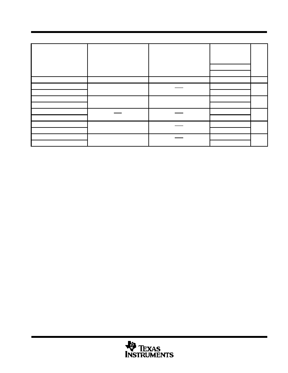
switching characteristics (see Figure 1)
PARAMETER
FROM
(INPUT)
TO
(OUTPUT)
VCC = 4.5 V to 5.5 V,
CL = 50 pF,
RL = 500
,
TA = MIN to MAX
UNIT
(INPUT)
(OUTPUT)
SN74ALS869
MIN
MAX
fmax
35
MHz
tPLH
CLK
RCO
4
14
ns
tPHL
CLK
RCO
4
14
ns
tPLH
CLK
Any Q
3
16
ns
tPHL
CLK
Any Q
3
16
ns
tPLH
ENT
RCO
3
14
ns
tPHL
ENT
RCO
2
9
ns
tPLH
S1
RCO
4
15
ns
tPHL
(count up/down)
RCO
4
15
ns
tPLH
S0
RCO
4
16
ns
tPHL
(clear/load)
RCO
4
12
ns
For conditions shown as MIN or MAX, use the appropriate value specified under recommended operating conditions.

SN54AS867, SN54AS869
SN74ALS867A, SN74ALS869, SN74AS867, SN74AS869
SYNCHRONOUS 8-BIT UP/DOWN COUNTERS
SDAS115C ≠ DECEMBER 1982 ≠ REVISED JANUARY 1995
12
POST OFFICE BOX 655303
∑
DALLAS, TEXAS 75265
absolute maximum ratings over operating free-air temperature range (unless otherwise noted)
Supply voltage, V
CC
7 V
. . . . . . . . . . . . . . . . . . . . . . . . . . . . . . . . . . . . . . . . . . . . . . . . . . . . . . . . . . . . . . . . . . . . . . . .
Input voltage, V
I
7 V
. . . . . . . . . . . . . . . . . . . . . . . . . . . . . . . . . . . . . . . . . . . . . . . . . . . . . . . . . . . . . . . . . . . . . . . . . . . .
Operating free-air temperature range, T
A
: SN54AS867
≠ 55
∞
C to 125
∞
C
. . . . . . . . . . . . . . . . . . . . . . . . . . . . . .
SN74AS867
0
∞
C to 70
∞
C
. . . . . . . . . . . . . . . . . . . . . . . . . . . . . . . . . .
Storage temperature range
≠ 65
∞
C to 150
∞
C
. . . . . . . . . . . . . . . . . . . . . . . . . . . . . . . . . . . . . . . . . . . . . . . . . . . . . . .
Stresses beyond those listed under "absolute maximum ratings" may cause permanent damage to the device. These are stress ratings only, and
functional operation of the device at these or any other conditions beyond those indicated under "recommended operating conditions" is not
implied. Exposure to absolute-maximum-rated conditions for extended periods may affect device reliability.
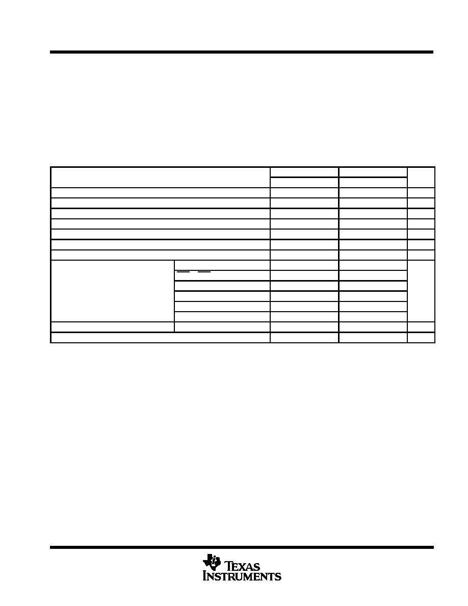
recommended operating conditions
SN54AS867
SN74AS867
UNIT
MIN
NOM
MAX
MIN
NOM
MAX
UNIT
VCC
Supply voltage
4.5
5
5.5
4.5
5
5.5
V
VIH
High-level input voltage
2
2
V
VIL
Low-level input voltage
0.8
0.8
V
IOH
High-level output current
≠ 2
≠ 2
mA
IOL
Low-level output current
20
20
mA
fclock*
Clock frequency
0
40
0
50
MHz
tw(clock)*
Pulse duration, CLK high or low
12.5
10
ns
tw(clear)*
Pulse duration of clear pulse, S0 and S1 low
12.5
10
ns
Data inputs A ≠ H
5
4
ENP or ENT
9
8
t
*
Set p time before CLK
S0 low and S1 high (load)
11
10
ns
tsu*
Setup time before CLK
S0 and S1 low (clear)
11
10
ns
S0 high and S1 low (count down)
42
40
S0 and S1 high (count up)
42
40
th*
Hold time after CLK
Data inputs A ≠ H
0
0
ns
tskew*
Skew time between S0 and S1
(maximum to avoid inadvertent clear)
8
7
ns
TA
Operating free-air temperature
≠ 55
125
0
70
∞
C
* On products compliant to MIL-STD-883, Class B, this parameter is based on characterization data but is not production tested.
SN54AS867, SN54AS869
SN74ALS867A, SN74ALS869, SN74AS867, SN74AS869
SYNCHRONOUS 8-BIT UP/DOWN COUNTERS
SDAS115C ≠ DECEMBER 1982 ≠ REVISED JANUARY 1995
13
POST OFFICE BOX 655303
∑
DALLAS, TEXAS 75265
electrical characteristics over recommended operating free-air temperature range (unless
otherwise noted)
PARAMETER
TEST CONDITIONS
SN54AS867
SN74AS867
UNIT
PARAMETER
TEST CONDITIONS
MIN
TYP
MAX
MIN
TYP
MAX
UNIT
VIK
VCC = 4.5 V,
II = ≠18 mA
≠1.2
≠1.2
V
VOH
VCC = 4.5 V to 5.5 V,
IOH = ≠ 2 mA
VCC ≠ 2
VCC ≠ 2
V
VOL
RCO
VCC = 4.5 V
IOL = 20 mA,
VIL on ENT = 0.7 V
0.34
0.5
V
OL
Other outputs
CC
IOL = 20 mA
0.34
0.5
II
VCC = 5.5 V,
VI = 7 V
0.1
0.1
mA
IIH
ENT
VCC = 5 5 V
VI = 2 7 V
40
40
µ
A
IIH
Other inputs
VCC = 5.5 V,
VI = 2.7 V
20
20
µ
A
IIL
ENT
VCC = 5 5 V
VI = 0 4 V
≠ 4
≠ 4
mA
IIL
Other inputs
VCC = 5.5 V,
VI = 0.4 V
≠ 2
≠ 2
mA
IO
VCC = 5.5 V,
VO = 2.25 V
≠ 30
≠ 112
≠ 30
≠ 112
mA
ICC
VCC = 5.5 V
134
195
134
195
mA
All typical values are at VCC = 5 V, TA = 25
∞
C.
The output conditions have been chosen to produce a current that closely approximates one half of the true short-circuit output current, IOS.
switching characteristics (see Figure 1)
PARAMETER
FROM
(INPUT)
TO
(OUTPUT)
VCC = 4.5 V to 5.5 V,
CL = 50 pF,
RL = 500
,
TA = MIN to MAXß
UNIT
(INPUT)
(OUTPUT)
SN54AS867
SN74AS867
MIN
MAX
MIN
MAX
fmax*
40
50
MHz
tPLH
CLK
RCO
5
31
5
22
ns
tPHL
CLK
RCO
6
19
6
16
ns
tPLH
CLK
Any Q
3
12
3
11
ns
tPHL
CLK
Any Q
4
16
4
15
ns
tPLH
ENT
RCO
3
19
3
10
ns
tPHL
ENT
RCO
5
21
5
17
ns
tPLH
ENP
RCO
5
16
5
14
ns
tPHL
ENP
RCO
5
21
5
17
ns
tPHL
Clear (S0 or S1 low)
Any Q
7
23
7
21
ns
* On products compliant to MIL-STD-883, Class B, this parameter is based on characterization data but is not production tested.
ß For conditions shown as MIN or MAX, use the appropriate value specified under recommended operating conditions.
SN54AS867, SN54AS869
SN74ALS867A, SN74ALS869, SN74AS867, SN74AS869
SYNCHRONOUS 8-BIT UP/DOWN COUNTERS
SDAS115C ≠ DECEMBER 1982 ≠ REVISED JANUARY 1995
14
POST OFFICE BOX 655303
∑
DALLAS, TEXAS 75265
absolute maximum ratings over operating free-air temperature range (unless otherwise noted)
Supply voltage, V
CC
7 V
. . . . . . . . . . . . . . . . . . . . . . . . . . . . . . . . . . . . . . . . . . . . . . . . . . . . . . . . . . . . . . . . . . . . . . . .
Input voltage, V
I
7 V
. . . . . . . . . . . . . . . . . . . . . . . . . . . . . . . . . . . . . . . . . . . . . . . . . . . . . . . . . . . . . . . . . . . . . . . . . . . .
Operating free-air temperature range, T
A
: SN54AS869
≠ 55
∞
C to 125
∞
C
. . . . . . . . . . . . . . . . . . . . . . . . . . . . . .
SN74AS869
0
∞
C to 70
∞
C
. . . . . . . . . . . . . . . . . . . . . . . . . . . . . . . . . .
Storage temperature range
≠ 65
∞
C to 150
∞
C
. . . . . . . . . . . . . . . . . . . . . . . . . . . . . . . . . . . . . . . . . . . . . . . . . . . . . . .
Stresses beyond those listed under "absolute maximum ratings" may cause permanent damage to the device. These are stress ratings only, and
functional operation of the device at these or any other conditions beyond those indicated under "recommended operating conditions" is not
implied. Exposure to absolute-maximum-rated conditions for extended periods may affect device reliability.
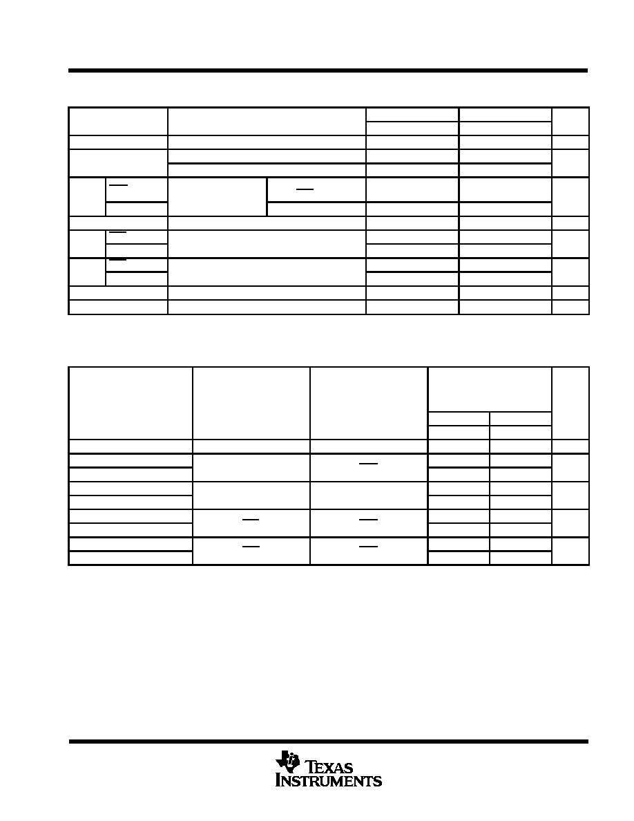
recommended operating conditions
SN54AS869
SN74AS869
UNIT
MIN
NOM
MAX
MIN
NOM
MAX
UNIT
VCC
Supply voltage
4.5
5
5.5
4.5
5
5.5
V
VIH
High-level input voltage
2
2
V
VIL
Low-level input voltage
0.7
0.8
V
IOH
High-level output current
≠ 2
≠ 2
mA
IOL
Low-level output current
20
20
mA
fclock*
Clock frequency
40
45
MHz
tw(clock)*
Pulse duration, CLK high or low
12.5
11
ns
Data inputs A ≠ H
6
5
ENP or ENT
10
9
t
*
Set p time before CLK
S0 low and S1 high (load)
13
11
ns
tsu*
Setup time before CLK
S0 and S1 low (clear)
13
11
ns
S0 high and S1 low (count down)
52
50
S0 and S1 high (count up)
52
50
th*
Hold time after CLK
Data inputs A ≠ H
0
0
ns
TA
Operating free-air temperature
≠ 55
125
0
70
∞
C
* On products compliant to MIL-STD-883, Class B, this parameter is based on characterization data but is not production tested.
SN54AS867, SN54AS869
SN74ALS867A, SN74ALS869, SN74AS867, SN74AS869
SYNCHRONOUS 8-BIT UP/DOWN COUNTERS
SDAS115C ≠ DECEMBER 1982 ≠ REVISED JANUARY 1995
15
POST OFFICE BOX 655303
∑
DALLAS, TEXAS 75265
electrical characteristics over recommended operating free-air temperature range (unless
otherwise noted)
PARAMETER
TEST CONDITIONS
SN54AS869
SN74AS869
UNIT
PARAMETER
TEST CONDITIONS
MIN
TYP
MAX
MIN
TYP
MAX
UNIT
VIK
VCC = 4.5 V,
II = ≠18 mA
≠1.2
≠1.2
V
VOH
VCC = 4.5 V to 5.5 V,
IOH = ≠ 2 mA
VCC ≠ 2
V
VOH
VCC = 4.5 V,
IOH = ≠ 2 mA
VCC ≠ 2*
V
VOL
RCO
VCC = 4.5 V
IOL = 20 mA,
VIL on ENT = 0.7 V
0.34
0.5
V
OL
Other outputs
CC
IOL = 20 mA
0.34
0.5
II
VCC = 5.5 V,
VI = 7 V
0.1
0.1
mA
IIH
ENT
VCC = 5 5 V
VI = 2 7 V
40
40
µ
A
IIH
Other inputs
VCC = 5.5 V,
VI = 2.7 V
20
20
µ
A
IIL
ENT
VCC = 5 5 V
VI = 0 4 V
≠ 4
≠ 4
mA
IIL
Other inputs
VCC = 5.5 V,
VI = 0.4 V
≠ 2
≠ 2
mA
IO
VCC = 5.5 V,
VO = 2.25 V
≠ 30
≠ 112
≠ 30
≠ 112
mA
ICC
VCC = 5.5 V
134
195
134
195
mA
All typical values are at VCC = 5 V, TA = 25
∞
C.
The output conditions have been chosen to produce a current that closely approximates one half of the true short-circuit output current, IOS.
switching characteristics (see Figure 1)
PARAMETER
FROM
(INPUT)
TO
(OUTPUT)
VCC = 4.5 V to 5.5 V,
CL = 50 pF,
RL = 500
,
TA = MIN to MAXß
UNIT
(INPUT)
(OUTPUT)
SN54AS869
SN74AS869
MIN
MAX
MIN
MAX
fmax*
40
45
MHz
tPLH
CLK
RCO
6
35
6
35
ns
tPHL
CLK
RCO
6
20
6
18
ns
tPLH
CLK
Any Q
3
12
3
11
ns
tPHL
CLK
Any Q
4
16
4
15
ns
tPLH
ENT
RCO
3
25
3
15
ns
tPHL
ENT
RCO
6
21
6
17
ns
tPLH
ENP
RCO
5
27
5
19
ns
tPHL
ENP
RCO
6
21
6
18
ns
* On products compliant to MIL-STD-883, Class B, this parameter is based on characterization data but is not production tested.
ß For conditions shown as MIN or MAX, use the appropriate value specified under recommended operating conditions.
SN54AS867, SN54AS869
SN74ALS867A, SN74ALS869, SN74AS867, SN74AS869
SYNCHRONOUS 8-BIT UP/DOWN COUNTERS
SDAS115C ≠ DECEMBER 1982 ≠ REVISED JANUARY 1995
16
POST OFFICE BOX 655303
∑
DALLAS, TEXAS 75265
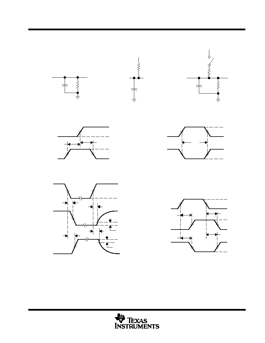
PARAMETER MEASUREMENT INFORMATION
SERIES 54ALS/ 74ALS AND 54AS/ 74AS DEVICES
tPHZ
tPLZ
tPHL
tPLH
0.3 V
tPZL
tPZH
tPLH
tPHL
LOAD CIRCUIT
FOR 3-STATE OUTPUTS
From Output
Under Test
Test
Point
R1
S1
CL
(see Note A)
7 V
1.3 V
1.3 V
1.3 V
3.5 V
3.5 V
0.3 V
0.3 V
th
tsu
VOLTAGE WAVEFORMS
SETUP AND HOLD TIMES
Timing
Input
Data
Input
1.3 V
1.3 V
3.5 V
3.5 V
0.3 V
0.3 V
High-Level
Pulse
Low-Level
Pulse
tw
VOLTAGE WAVEFORMS
PULSE DURATIONS
Input
Out-of-Phase
Output
(see Note C)
1.3 V
1.3 V
1.3 V
1.3 V
1.3 V
1.3 V
1.3 V
1.3 V
1.3 V
1.3 V
3.5 V
3.5 V
0.3 V
0.3 V
VOL
VOH
VOH
VOL
Output
Control
(low-level
enabling)
Waveform 1
S1 Closed
(see Note B)
Waveform 2
S1 Open
(see Note B)
[
0 V
VOH
VOL
[
3.5 V
In-Phase
Output
0.3 V
1.3 V
1.3 V
VOLTAGE WAVEFORMS
PROPAGATION DELAY TIMES
VOLTAGE WAVEFORMS
ENABLE AND DISABLE TIMES, 3-STATE OUTPUTS
R2
VCC
RL
Test
Point
From Output
Under Test
CL
(see Note A)
LOAD CIRCUIT
FOR OPEN-COLLECTOR OUTPUTS
LOAD CIRCUIT FOR
BI-STATE
TOTEM-POLE OUTPUTS
From Output
Under Test
Test
Point
CL
(see Note A)
RL
RL = R1 = R2
NOTES: A. CL includes probe and jig capacitance.
B. Waveform 1 is for an output with internal conditions such that the output is low except when disabled by the output control.
Waveform 2 is for an output with internal conditions such that the output is high except when disabled by the output control.
C. When measuring propagation delay items of 3-state outputs, switch S1 is open.
D. All input pulses have the following characteristics: PRR
1 MHz, tr = tf = 2 ns, duty cycle = 50%.
E. The outputs are measured one at a time with one transition per measurement.
Figure 1. Load Circuits and Voltage Waveforms

IMPORTANT NOTICE
Texas Instruments and its subsidiaries (TI) reserve the right to make changes to their products or to discontinue
any product or service without notice, and advise customers to obtain the latest version of relevant information
to verify, before placing orders, that information being relied on is current and complete. All products are sold
subject to the terms and conditions of sale supplied at the time of order acknowledgement, including those
pertaining to warranty, patent infringement, and limitation of liability.
TI warrants performance of its semiconductor products to the specifications applicable at the time of sale in
accordance with TI's standard warranty. Testing and other quality control techniques are utilized to the extent
TI deems necessary to support this warranty. Specific testing of all parameters of each device is not necessarily
performed, except those mandated by government requirements.
CERTAIN APPLICATIONS USING SEMICONDUCTOR PRODUCTS MAY INVOLVE POTENTIAL RISKS OF
DEATH, PERSONAL INJURY, OR SEVERE PROPERTY OR ENVIRONMENTAL DAMAGE ("CRITICAL
APPLICATIONS"). TI SEMICONDUCTOR PRODUCTS ARE NOT DESIGNED, AUTHORIZED, OR
WARRANTED TO BE SUITABLE FOR USE IN LIFE-SUPPORT DEVICES OR SYSTEMS OR OTHER
CRITICAL APPLICATIONS. INCLUSION OF TI PRODUCTS IN SUCH APPLICATIONS IS UNDERSTOOD TO
BE FULLY AT THE CUSTOMER'S RISK.
In order to minimize risks associated with the customer's applications, adequate design and operating
safeguards must be provided by the customer to minimize inherent or procedural hazards.
TI assumes no liability for applications assistance or customer product design. TI does not warrant or represent
that any license, either express or implied, is granted under any patent right, copyright, mask work right, or other
intellectual property right of TI covering or relating to any combination, machine, or process in which such
semiconductor products or services might be or are used. TI's publication of information regarding any third
party's products or services does not constitute TI's approval, warranty or endorsement thereof.
Copyright
©
1998, Texas Instruments Incorporated