
LT1014, LT1014A, LT1014D
QUAD PRECISION OPERATIONAL AMPLIFIERS
SLOS039C ≠ JULY 1989 ≠ REVISED SEPTEMBER 1999
1
POST OFFICE BOX 655303
∑
DALLAS, TEXAS 75265
D
Single-Supply Operation:
Input Voltage Range Extends to Ground,
and Output Swings to Ground While
Sinking Current
D
Input Offset Voltage 300
µ
V Max at 25
∞
C for
LT1014
D
Offset Voltage Temperature Coefficient
2.5
µ
V/
∞
C Max for LT1014
D
Input Offset Current 1.5 nA Max at 25
∞
C for
LT1014
D
High Gain 1.2 V/
µ
V Min (R
L
= 2 k
), 0.5 V/
µ
V
Min (R
L
= 600
) for LT1014
D
Low Supply Current 2.2 mA Max at 25
∞
C for
LT 1014
D
Low Peak-to-Peak Noise Voltage
0.55
µ
V Typ
D
Low Current Noise 0.07 pA/
Hz Typ
description
The LT1014, LT1014A, and LT1014D are quad
precision operational amplifiers with 14-pin
industry-standard configuration. They feature low
offset-voltage temperature coefficient, high gain,
low supply current, and low noise.
The LT1014, LT1014A, and LT1014D can be
operated with both dual
±
15 V and single 5 V
power supplies.
The common-mode input voltage
range includes ground, and the output voltage can
also swing to within a few milivolts of ground.
Crossover distortion is eliminated.
The LT1014C and LT1014 AC are characterized
for operation from 0
∞
C to 70
∞
C. The LT1014I and
LT1014DI are characterized for operation from
≠40
∞
C to 105
∞
C. The LT1014M, LT1014AM and
LT1014DM are characterized for operation over
the full military temperature range of ≠55
∞
C to
125
∞
C.
Copyright
©
1999, Texas Instruments Incorporated
PRODUCTION DATA information is current as of publication date.
Products conform to specifications per the terms of Texas Instruments
standard warranty. Production processing does not necessarily include
testing of all parameters.
Please be aware that an important notice concerning availability, standard warranty, and use in critical applications of
Texas Instruments semiconductor products and disclaimers thereto appears at the end of this data sheet.
1
2
3
4
5
6
7
8
16
15
14
13
12
11
10
9
1OUT
1IN≠
1IN+
V
CC+
2IN+
2IN≠
2OUT
NC
4OUT
4IN≠
4IN+
V
CC≠
/GND
3IN+
3IN≠
3OUT
NC
DW PACKAGE
(TOP VIEW)
1
2
3
4
5
6
7
14
13
12
11
10
9
8
1OUT
1IN≠
1IN+
V
CC+
2IN+
2IN≠
2OUT
4OUT
4IN≠
4IN+
V
CC≠
3IN+
3IN≠
3OUT
3
2
1 20 19
9 10 11 12 13
4
5
6
7
8
18
17
16
15
14
4IN+
NC
V
CC≠
/GND
NC
3IN+
1IN+
NC
V
CC+
NC
2IN+
1IN≠
1OUT
NC
3IN≠
4IN≠
2IN≠
2OUT
NC
3OUT
4OUT
J OR N PACKAGE
(TOP VIEW)
FK PACKAGE
(TOP VIEW)
NC ≠ No internal connection

LT1014, LT1014A, LT1014D
QUAD PRECISION OPERATIONAL AMPLIFIERS
SLOS039C ≠ JULY 1989 ≠ REVISED SEPTEMBER 1999
2
POST OFFICE BOX 655303
∑
DALLAS, TEXAS 75265
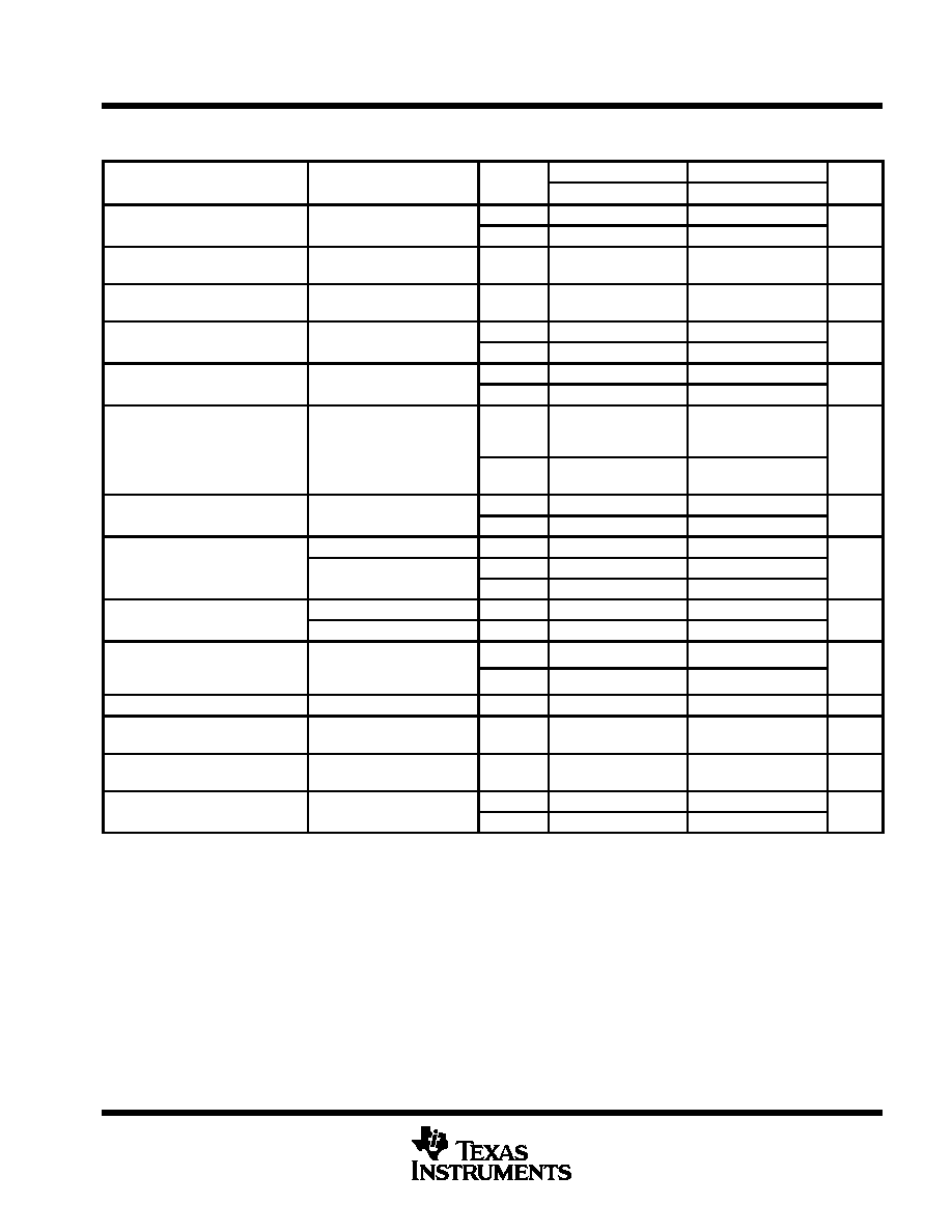
AVAILABLE OPTIONS
PACKAGED DEVICES
TA
VIO max
AT 25
∞
C
SMALL
OUTLINE
(DW)
CHIP
CARRIER
(FK)
CERAMIC
DIP
(J)
PLASTIC
DIP
(N)
0
∞
C to 70
∞
C
300
µ
V
--
--
--
LT1014CN
0
∞
C to 70
∞
C
µ
800
µ
V
LT1014DDW
--
--
LT1014DN
40
∞
C to 105
∞
C
300
µ
V
--
--
--
LT1014IN
≠40
∞
C to 105
∞
C
µ
800
µ
V
LT1014DIDW
--
--
LT1014DIN
180
µ
V
--
LT1014AMFK
LT1014AMJ
--
≠55
∞
C to 125
∞
C
180
µ
V
300
µ
V
--
LT1014AMFK
LT1014MFK
LT1014AMJ
LT1014MJ
LT1014MN
µ
800
µ
V
LT1014DMDW
--
--
LT1014DMN
The DW package is available taped and reeled. Add the suffix R to the device type (e.g., LT1014DDWR).

LT1014, LT1014A, LT1014D
QUAD PRECISION OPERATIONAL AMPLIFIERS
SLOS039C ≠ JULY 1989 ≠ REVISED SEPTEMBER 1999
3
POST OFFICE BOX 655303
∑
DALLAS, TEXAS 75265
schematic (each amplifier)
V
CC+
IN≠
IN+
V
CC≠
k
9
k
9
k
1.6
k
1.6
k
1.6
100
k
1
800
Q5
Q6
Q13
Q16
Q14
Q15
Q32
Q30
Q25
Q35
Q36
Q41
Q39
600
Q3
Q4
Q37
J1
Q33
Q26
k
3.9
Q27
Q38
Q28
Q2
Q22
Q1
Q21
400
400
Q12
Q1
1
Q9
75 pF
Q7
Q29
Q10
Q18
Q19
Q17
21 pF
2.5 pF
k
2.4
18
k
14
OUT
Q40
Q8
k
5
k
5
10 pF
k
2
k
1.3
Q20
4 pF
Q31
Q34
Q23
Q24
k
2
10 pF
k
2
30
k
42
Component values are nominal.
LT1014, LT1014A, LT1014D
QUAD PRECISION OPERATIONAL AMPLIFIERS
SLOS039C ≠ JULY 1989 ≠ REVISED SEPTEMBER 1999
4
POST OFFICE BOX 655303
∑
DALLAS, TEXAS 75265
absolute maximum ratings over operating free-air temperature range (unless otherwise noted)
Supply voltage (see Note 1): V
CC+
22 V
. . . . . . . . . . . . . . . . . . . . . . . . . . . . . . . . . . . . . . . . . . . . . . . . . . . . . . . . . .
V
CC≠
≠22
V
. . . . . . . . . . . . . . . . . . . . . . . . . . . . . . . . . . . . . . . . . . . . . . . . . . . . . . . . . .
Differential input voltage (see Note 2)
±
30 V
. . . . . . . . . . . . . . . . . . . . . . . . . . . . . . . . . . . . . . . . . . . . . . . . . . . . . . . .
Input voltage range, V
I
(any input) (see Note 1)
V
CC≠
≠ 5 V to V
CC+
. . . . . . . . . . . . . . . . . . . . . . . . . . . . . . . . . .
Duration of short-circuit current at (or below) T
A
= 25
∞
C (see Note 3)
Unlimited
. . . . . . . . . . . . . . . . . . . . . . . . .
Continuous total power dissipation
See Dissipation Rating Table
. . . . . . . . . . . . . . . . . . . . . . . . . . . . . . . . . . . . .
Operating free-air temperature range, T
A
: LT1014C, LT1014DC
≠0
∞
C to 70
∞
C
. . . . . . . . . . . . . . . . . . . . . . . . . .
LT1014I, LT1014DI
≠40
∞
C to 105
∞
C
. . . . . . . . . . . . . . . . . . . . . . . . . .
LT1014M, LT1014AM, LT1014DM
≠55
∞
C to 125
∞
C
. . . . . . . . . . . . .
Lead temperature 1,6 mm (1/16 inch) from case for 60 seconds: J package
300
∞
C
. . . . . . . . . . . . . . . . . . . . .
Lead temperature 1,6 mm (1/16 inch) from case for 10 seconds: DW or N package
260
∞
C
. . . . . . . . . . . . . . .
Case temperature for 60 seconds: FK package
260
∞
C
. . . . . . . . . . . . . . . . . . . . . . . . . . . . . . . . . . . . . . . . . . . . . .
Storage temperature range, T
stg
≠65
∞
C to 150
∞
C
. . . . . . . . . . . . . . . . . . . . . . . . . . . . . . . . . . . . . . . . . . . . . . . . . . .
Stresses beyond those listed under "absolute maximum ratings" may cause permanent damage to the device. These are stress ratings only, and
functional operation of the device at these or any other conditions beyond those indicated under "recommended operating conditions" is not
implied. Exposure to absolute-maximum-rated conditions for extended periods may affect device reliability.
NOTES:
1. All voltage values, except differential voltages, are with respect to the midpoint between VCC+ and VCC≠.
2. Differential voltages are at the noninverting input with respect to the inverting input.
3. The output may be shorted to either supply.
DISSIPATION RATING TABLE
PACKAGE
TA
25
∞
C
POWER RATING
DERATING FACTOR
ABOVE TA = 25
∞
C
TA = 70
∞
C
POWER RATING
TA = 105
∞
C
POWER RATING
TA = 125
∞
C
POWER RATING
DW
1025 mV
8.2 mW/
∞
C
656 mW
369 mW
205 mW
FK
1375 mV
11.0 mW/
∞
C
880 mW
495 mW
275 mW
J
1375 mV
11.0 mW/
∞
C
880 mW
495 mW
275 mW
N
1150 mV
9.2 mW/
∞
C
736 mW
414 mW
230 mW
LT1014, LT1014A, LT1014D
QUAD PRECISION OPERATIONAL AMPLIFIERS
SLOS039C ≠ JULY 1989 ≠ REVISED SEPTEMBER 1999
5
POST OFFICE BOX 655303
∑
DALLAS, TEXAS 75265
electrical characteristics at specified free-air temperature, V
CC
±
=
±
15 V, V
IC
= 0 (unless otherwise
noted)
PARAMETER
TEST CONDITIONS
T
LT1014C
LT1014DC
UNIT
PARAMETER
TEST CONDITIONS
TA
MIN
TYP
MAX
MIN
TYP
MAX
UNIT
VIO
Input offset voltage
RS = 50
25
∞
C
60
300
200
800
µ
V
VIO
Input offset voltage
RS = 50
Full range
550
1000
µ
V
a
V
IO
Temperature coeficient
of input offset voltage
Full range
0.4
2.5
0.7
5
µ
V/
∞
C
Long-term drift
of input offset voltage
25
∞
C
0.5
0.5
µ
V/mo
IIO
Input offset current
25
∞
C
0.15
1.5
0.15
1.5
nA
IIO
Input offset current
Full range
2.8
2.8
nA
IIB
Input bias current
25
∞
C
≠12
≠30
≠12
≠30
nA
IIB
Input bias current
Full range
≠38
≠38
nA
VICR
Common-mode
input voltage range
25
∞
C
≠15
to
13.5
≠15.3
to
13.8
≠15
to
13.5
≠15.3
to
13.8
V
ICR
input voltage range
Full range
≠15
to 13
≠15
to 13
VOM
Maximum peak output
RL = 2 k
25
∞
C
±
12.5
±
14
±
12.5
±
14
V
VOM
voltage swing
RL = 2 k
Full range
±
12
±
12
V
L
i
l diff
ti l
VO =
±
10 V,
RL = 600
25
∞
C
0.5
2
0.5
2
AVD
Large-signal differential
voltage amplification
VO =
±
10 V
RL = 2 k
25
∞
C
1.2
8
1.2
8
V/
µ
V
voltage am lification
VO =
±
10 V,
RL = 2 k
Full range
0.7
0.7
CMRR
Common-mode
VIC = ≠15 V to 13.5 V
25
∞
C
97
117
97
117
dB
CMRR
rejection ratio
VIC = ≠15 V to 13 V
Full range
94
94
dB
kSVR
Supply-voltage
rejection ratio
VCC
±
=
±
2 V to
±
18 V
25
∞
C
100
117
100
117
dB
kSVR
rejection ratio
(
VCC/
VIO)
VCC
±
=
±
2 V to
±
18 V
Full range
97
97
dB
Channel separation
VO =
±
10 V,
RL = 2 k
25
∞
C
120
137
120
137
dB
rid
Differential
input resistance
25
∞
C
70
300
70
300
M
ric
Common-mode
input resistance
25
∞
C
4
4
G
ICC
Supply current
25
∞
C
0.35
0.55
0.35
0.55
mA
ICC
y
per amplifier
Full range
0.6
0.6
mA
Full range is 0
∞
C to 70
∞
C.
All typical values are at TA = 25
∞
C.