
SN54AS756, SN74AS756, SN74AS757
OCTAL BUFFERS AND LINE DRIVERS
WITH OPEN-COLLECTOR OUTPUTS
SDAS040B ≠ DECEMBER 1983 ≠ REVISED JANUARY 1995
Copyright
©
1995, Texas Instruments Incorporated
1
POST OFFICE BOX 655303
∑
DALLAS, TEXAS 75265
∑
Open-Collector Outputs Drive Bus Lines or
Buffer Memory Address Registers
∑
Eliminate the Need for 3-State Overlap
Protection
∑
pnp Inputs Reduce dc Loading
∑
Open-Collector Versions of
AS240A and
AS241
∑
Package Options Include Plastic
Small-Outline (DW) Packages, Ceramic
Chip Carriers (FK), and Standard Plastic (N)
and Ceramic (J) 300-mil DIPs
description
These octal buffers and line drivers are designed
specifically to improve the performance and
density of 3-state memory address drivers, clock
drivers, and bus-oriented receivers and
transmitters by eliminating the need for 3-state
overlap protection. The designer has a choice of
selected combinations of inverting and
noninverting outputs, symmetrical active-low
output-enable (OE) inputs, and complementary
OE and OE inputs. These devices feature high
fan-out and improved fan-in.
The SN54AS756 is characterized for operation
over the full military temperature range of ≠ 55
∞
C
to 125
∞
C. The SN74AS756 and SN74AS757 are
characterized for operation from 0
∞
C to 70
∞
C.
logic symbols
2
1A1
4
1A2
6
1A3
8
1A4
EN
1
1Y1
18
1Y2
16
1Y3
14
1Y4
12
11
2A1
13
2A2
15
2A3
17
2A4
EN
19
2Y1
9
2Y2
7
2Y3
5
2Y4
3
1OE
2OE
AS756
2
1A1
4
1A2
6
1A3
8
1A4
EN
1
1Y1
18
1Y2
16
1Y3
14
1Y4
12
11
2A1
13
2A2
15
2A3
17
2A4
EN
19
2OE
2Y1
9
2Y2
7
2Y3
5
2Y4
3
1OE
SN74AS757
These symbols are in accordance with ANSI/IEEE Std 91-1984 and IEC Publication 617-12.
1
2
3
4
5
6
7
8
9
10
20
19
18
17
16
15
14
13
12
11
1OE
1A1
2Y4
1A2
2Y3
1A3
2Y2
1A4
2Y1
GND
V
CC
2OE / 2OE
1Y1
2A4
1Y2
2A3
1Y3
2A2
1Y4
2A1
SN54AS756 . . . J PACKAGE
SN74AS756, SN74AS757 . . . DW OR N PACKAGE
(TOP VIEW)
3
2
1 20 19
9 10 11 12 13
4
5
6
7
8
18
17
16
15
14
1Y1
2A4
1Y2
2A3
1Y3
1A2
2Y3
1A3
2Y2
1A4
SN54AS756 . . . FK PACKAGE
(TOP VIEW)
2Y4
1A1
1OE
1Y4
2A2
2OE
2Y1
GND
2A1
V
CC
2OE for
AS756 or 2OE for SN74AS757
PRODUCTION DATA information is current as of publication date.
Products conform to specifications per the terms of Texas Instruments
standard warranty. Production processing does not necessarily include
testing of all parameters.
SN54AS756, SN74AS756, SN74AS757
OCTAL BUFFERS AND LINE DRIVERS
WITH OPEN-COLLECTOR OUTPUTS
SDAS040B ≠ DECEMBER 1983 ≠ REVISED JANUARY 1995
2
POST OFFICE BOX 655303
∑
DALLAS, TEXAS 75265
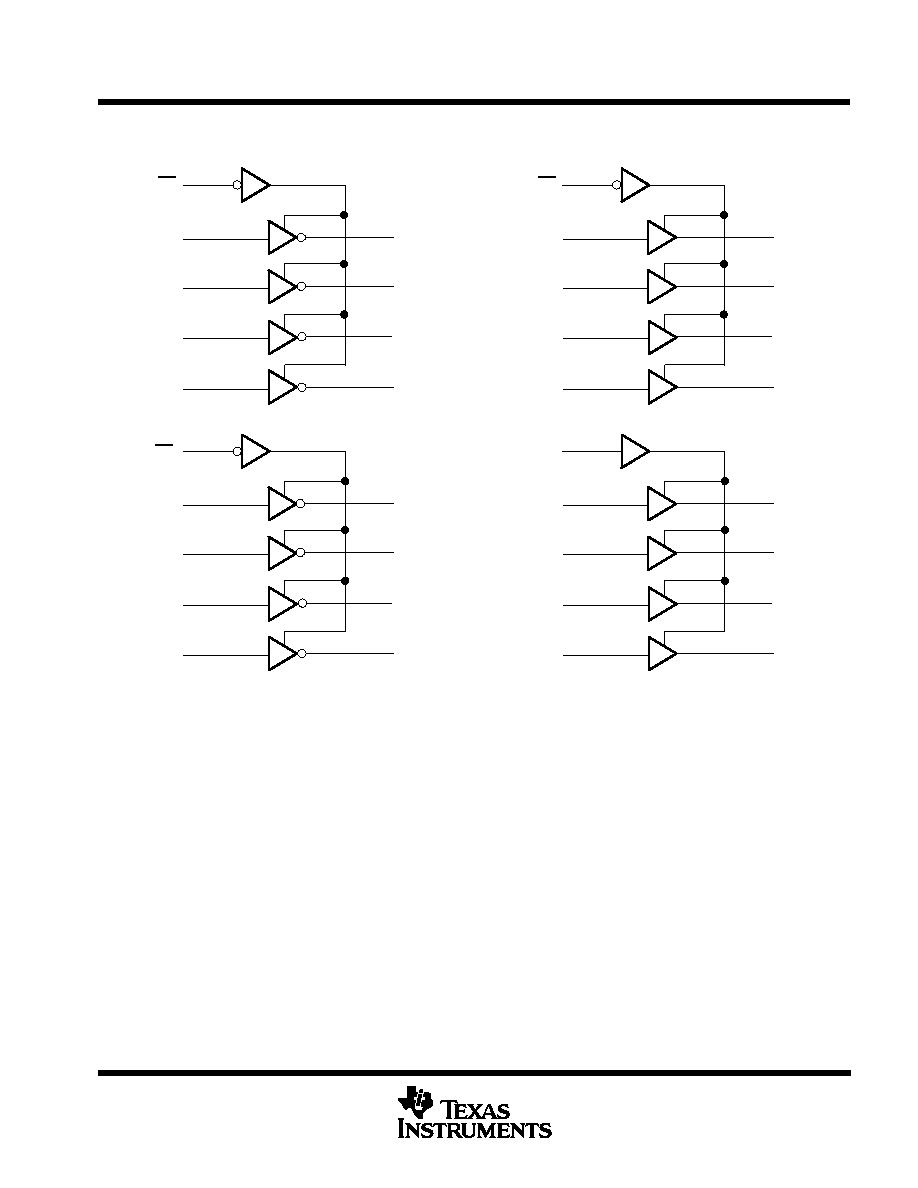
logic diagrams (positive logic)
1
2
4
6
8
19
11
13
15
17
3
5
7
9
12
14
16
18
1A1
1A2
1A3
1A4
1Y1
2A1
2A2
2A3
2A4
2Y1
1Y2
1Y3
1Y4
2Y2
2Y3
2Y4
1OE
2OE
1
2
4
6
8
19
11
13
15
17
3
5
7
9
12
14
16
18
1A1
1A2
1A3
1A4
1Y1
2A1
2A2
2A3
2A4
2Y1
1Y2
1Y3
1Y4
2Y2
2Y3
2Y4
1OE
2OE
AS756
SN74AS757
absolute maximum ratings over operating free-air temperature range (unless otherwise noted)
Supply voltage, V
CC
7 V
. . . . . . . . . . . . . . . . . . . . . . . . . . . . . . . . . . . . . . . . . . . . . . . . . . . . . . . . . . . . . . . . . . . . . . . .
Input voltage, V
I
7 V
. . . . . . . . . . . . . . . . . . . . . . . . . . . . . . . . . . . . . . . . . . . . . . . . . . . . . . . . . . . . . . . . . . . . . . . . . . . .
Off-state output voltage
7 V
. . . . . . . . . . . . . . . . . . . . . . . . . . . . . . . . . . . . . . . . . . . . . . . . . . . . . . . . . . . . . . . . . . . . . .
Operating free-air temperature range, T
A
: SN54AS756
≠ 55
∞
C to 125
∞
C
. . . . . . . . . . . . . . . . . . . . . . . . . . . . . .
SN74AS756, SN74AS757
0
∞
C to 70
∞
C
. . . . . . . . . . . . . . . . . . . . . .
Storage temperature range
≠ 65
∞
C to 150
∞
C
. . . . . . . . . . . . . . . . . . . . . . . . . . . . . . . . . . . . . . . . . . . . . . . . . . . . . . .
Stresses beyond those listed under "absolute maximum ratings" may cause permanent damage to the device. These are stress ratings only, and
functional operation of the device at these or any other conditions beyond those indicated under "recommended operating conditions" is not
implied. Exposure to absolute-maximum-rated conditions for extended periods may affect device reliability.

SN54AS756, SN74AS756, SN74AS757
OCTAL BUFFERS AND LINE DRIVERS
WITH OPEN-COLLECTOR OUTPUTS
SDAS040B ≠ DECEMBER 1983 ≠ REVISED JANUARY 1995
3
POST OFFICE BOX 655303
∑
DALLAS, TEXAS 75265
recommended operating conditions
SN54AS756
SN74AS756
SN74AS757
UNIT
MIN
NOM
MAX
MIN
NOM
MAX
VCC
Supply voltage
4.5
5
5.5
4.5
5
5.5
V
VIH
High-level input voltage
2
2
V
VIL
Low-level input voltage
0.7
0.8
V
VOH
High-level output voltage
5.5
5.5
V
IOL
Low-level output current
48
64
mA
TA
Operating free-air temperature
≠ 55
125
0
70
∞
C
electrical characteristics over recommended operating free-air temperature range (unless
otherwise noted)
PARAMETER
TEST CONDITIONS
SN54AS756
SN74AS756
SN74AS757
UNIT
MIN
TYP
MAX
MIN
TYP
MAX
VIK
VCC = 4.5 V,
II = ≠ 18 mA
≠ 1.2
≠ 1.2
V
IOH
VCC = 4.5 V,
VOH = 5.5 V
0.1
0.1
mA
VOL
VCC = 4 5 V
IOL = 48 mA
0.55
V
VOL
VCC = 4.5 V
IOL = 64 mA
0.55
V
II
VCC = 5.5 V,
VI = 7 V
0.1
0.1
mA
IIH
VCC = 5.5 V,
VI = 2.7 V
20
20
µ
A
IIL
A inputs of
SN74AS757 only
VCC = 5.5 V,
VI = 0.4 V
≠ 1
≠ 1
mA
IL
All other inputs
CC
,
I
≠ 0.5
≠ 0.5
AS756
VCC = 5 5 V
Outputs high
9
15
9
15
ICC
AS756
VCC = 5.5 V
Outputs low
51
80
51
80
mA
ICC
SN74AS757
VCC = 5 5 V
Outputs high
21
33
21
33
mA
SN74AS757
VCC = 5.5 V
Outputs low
61
95
61
95
All typical values are at VCC = 5 V, TA = 25
∞
C.

SN54AS756, SN74AS756, SN74AS757
OCTAL BUFFERS AND LINE DRIVERS
WITH OPEN-COLLECTOR OUTPUTS
SDAS040B ≠ DECEMBER 1983 ≠ REVISED JANUARY 1995
4
POST OFFICE BOX 655303
∑
DALLAS, TEXAS 75265
switching characteristics (see Figure 1)
PARAMETER
FROM
(INPUT)
TO
(OUTPUT)
VCC = 4.5 V to 5.5 V,
CL = 50 pF,
RL = 500
,
TA = MIN to MAX
UNIT
(INPUT)
(OUTPUT)
SN54AS756
SN74AS756
MIN
MAX
MIN
MAX
tPLH
A
Y
3
20
3
19
ns
tPHL
A
Y
1
7
1
6
ns
tPLH
OE
Y
3
22
3
19.5
ns
tPHL
OE
Y
1
8.5
1
7.5
ns
For conditions shown as MIN or MAX, use the appropriate value specified under recommended operating conditions.
switching characteristics (see Figure 1)
PARAMETER
FROM
(INPUT)
TO
(OUTPUT)
VCC = 4.5 V to 5.5 V,
CL = 50 pF,
RL = 500
,
TA = MIN to MAX
UNIT
(INPUT)
(OUTPUT)
SN74AS757
MIN
MAX
tPLH
A
Y
3
18.5
ns
tPHL
A
Y
1
6
ns
tPLH
1OE
1Y
3
20
ns
tPHL
1OE
1Y
1
7
ns
tPLH
2OE
2Y
3
21
ns
tPHL
2OE
2Y
1
7.5
ns
For conditions shown as MIN or MAX, use the appropriate value specified under recommended operating conditions.

SN54AS756, SN74AS756, SN74AS757
OCTAL BUFFERS AND LINE DRIVERS
WITH OPEN-COLLECTOR OUTPUTS
SDAS040B ≠ DECEMBER 1983 ≠ REVISED JANUARY 1995
5
POST OFFICE BOX 655303
∑
DALLAS, TEXAS 75265
PARAMETER MEASUREMENT INFORMATION
SERIES 54ALS/ 74ALS AND 54AS/ 74AS DEVICES
tPHZ
tPLZ
tPHL
tPLH
0.3 V
tPZL
tPZH
tPLH
tPHL
LOAD CIRCUIT
FOR 3-STATE OUTPUTS
From Output
Under Test
Test
Point
R1
S1
CL
(see Note A)
7 V
1.3 V
1.3 V
1.3 V
3.5 V
3.5 V
0.3 V
0.3 V
th
tsu
VOLTAGE WAVEFORMS
SETUP AND HOLD TIMES
Timing
Input
Data
Input
1.3 V
1.3 V
3.5 V
3.5 V
0.3 V
0.3 V
High-Level
Pulse
Low-Level
Pulse
tw
VOLTAGE WAVEFORMS
PULSE DURATIONS
Input
Out-of-Phase
Output
(see Note C)
1.3 V
1.3 V
1.3 V
1.3 V
1.3 V
1.3 V
1.3 V
1.3 V
1.3 V
1.3 V
3.5 V
3.5 V
0.3 V
0.3 V
VOL
VOH
VOH
VOL
Output
Control
(low-level
enabling)
Waveform 1
S1 Closed
(see Note B)
Waveform 2
S1 Open
(see Note B)
[
0 V
VOH
VOL
[
3.5 V
In-Phase
Output
0.3 V
1.3 V
1.3 V
VOLTAGE WAVEFORMS
PROPAGATION DELAY TIMES
VOLTAGE WAVEFORMS
ENABLE AND DISABLE TIMES, 3-STATE OUTPUTS
R2
VCC
RL
Test
Point
From Output
Under Test
CL
(see Note A)
LOAD CIRCUIT
FOR OPEN-COLLECTOR OUTPUTS
LOAD CIRCUIT FOR
BI-STATE
TOTEM-POLE OUTPUTS
From Output
Under Test
Test
Point
CL
(see Note A)
RL
RL = R1 = R2
NOTES: A. CL includes probe and jig capacitance.
B. Waveform 1 is for an output with internal conditions such that the output is low except when disabled by the output control.
Waveform 2 is for an output with internal conditions such that the output is high except when disabled by the output control.
C. When measuring propagation delay items of 3-state outputs, switch S1 is open.
D. All input pulses have the following characteristics: PRR
1 MHz, tr = tf = 2 ns, duty cycle = 50%.
E. The outputs are measured one at a time with one transition per measurement.
Figure 1. Load Circuits and Voltage Waveforms