1
Data sheet acquired from Harris Semiconductor
SCHS140E
Features
∑ Asynchronous Set and Reset
∑ Schmitt Trigger Clock Inputs
∑ Typical f
MAX
= 54MHz at V
CC
= 5V, C
L
= 15pF,
T
A
= 25
o
C
∑ Fanout (Over Temperature Range)
- Standard Outputs . . . . . . . . . . . . . . . 10 LSTTL Loads
- Bus Driver Outputs . . . . . . . . . . . . . 15 LSTTL Loads
∑ Wide Operating Temperature Range . . . -55
o
C to 125
o
C
∑ Balanced Propagation Delay and Transition Times
∑ Significant Power Reduction Compared to LSTTL
Logic ICs
∑ HC Types
- 2V to 6V Operation
- High Noise Immunity: N
IL
= 30%, N
IH
= 30% of V
CC
at V
CC
= 5V
∑ HCT Types
- 4.5V to 5.5V Operation
- Direct LSTTL Input Logic Compatibility,
V
IL
= 0.8V (Max), V
IH
= 2V (Min)
- CMOS Input Compatibility, I
l
1
µ
A at V
OL
, V
OH
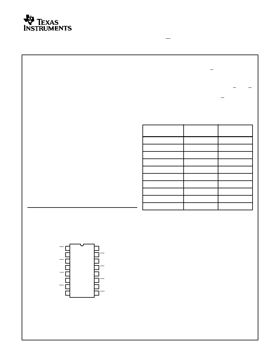
Pinout
CD54HC109, CD54HCT109
(CERDIP)
CD74HC109, CD74HCT109
(PDIP, SOIC)
TOP VIEW
Description
The 'HC109 and 'HCT109 are dual J-K flip-flops with set and
reset. The flip-flop changes state with the positive transition
of Clock (1CP and 2CP).
The flip-flop is set and reset by active-low S and R,
respectively. A low on both the set and reset inputs
simultaneously will force both Q and Q outputs high.
However, both set and reset going high simultaneously
results in an unpredictable output condition.
14
15
16
9
13
12
11
10
1
2
3
4
5
7
6
8
1R
1J
1K
1CP
1S
1Q
GND
1Q
V
CC
2J
2K
2CP
2S
2Q
2Q
2R
Ordering Information
PART NUMBER
TEMP. RANGE
(
o
C)
PACKAGE
CD54HC109F3A
-55 to 125
16 Ld CERDIP
CD54HCT109F3A
-55 to 125
16 Ld CERDIP
CD74HC109E
-55 to 125
16 Ld PDIP
CD74HC109M
-55 to 125
16 Ld SOIC
CD74HC109MT
-55 to 125
16 Ld SOIC
CD74HC109M96
-55 to 125
16 Ld SOIC
CD74HCT109E
-55 to 125
16 Ld PDIP
CD74HCT109M
-55 to 125
16 Ld SOIC
CD74HCT109MT
-55 to 125
16 Ld SOIC
CD74HCT109M96
-55 to 125
16 Ld SOIC
NOTE: When ordering, use the entire part number. The suffix 96
denotes tape and reel. The suffix T denotes a small-quantity reel of
250.
March 1998 - Revised October 2003
CAUTION: These devices are sensitive to electrostatic discharge. Users should follow proper IC Handling Procedures.
Copyright
©
2003, Texas Instruments Incorporated
CD54HC109, CD74HC109,
CD54HCT109, CD74HCT109
Dual J-K Flip-Flop with Set and Reset
Positive-Edge Trigger
[ /Title
(CD74H
C109,
CD74H
CT109)
/Subject
(Dual J-
K Flip-
Flop
with Set
and
Reset

2
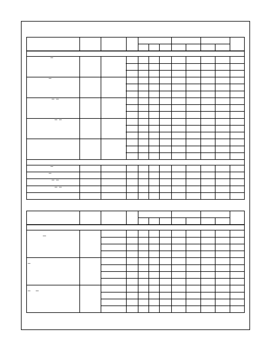
Functional Diagram
Logic Diagram
TRUTH TABLE
INPUTS
OUTPUTS
S
R
CP
J
K
Q
Q
L
H
X
X
X
H
L
H
L
X
X
X
L
H
L
L
X
X
X
H (Note 1)
H (Note 1)
H
H
L
L
L
H
H
H
H
L
Toggle
H
H
L
H
No Change
H
H
H
H
H
L
H
H
L
X
X
No Change
H= High Level (Steady State)
L= Low Level (Steady State)
X= Don't Care
= Low-to-High Transition
NOTE:
1. Unpredictable and unstable condition if both S and R go high simultaneously
1S
2S
2R
5
11
6
7
1Q
1Q
15
1
1R
2K
13
12
10
9
2Q
2Q
2CP
F/F 1
F/F 2
GND = 8
V
CC
= 16
2J
14
1K
3
4
1CP
1J
2
S
J
K
CL
CL
R
Q
Q
6(10)
7(9)
Q
Q
5(11)
S
2(14)
J
3(13)
K
4(12)
CP
1(15)
R
FF
V
CC
GND
16
8
CD54HC109, CD74HC109, CD54HCT109, CD74HCT109

3
Absolute Maximum Ratings
Thermal Information
DC Supply Voltage, V
CC
. . . . . . . . . . . . . . . . . . . . . . . . -0.5V to 7V
DC Input Diode Current, I
IK
For V
I
< -0.5V or V
I
> V
CC
+ 0.5V
. . . . . . . . . . . . . . . . . . . . . .±
20mA
DC Drain Current, per Output, I
O
For -0.5V < V
O
< V
CC
+ 0.5V
. . . . . . . . . . . . . . . . . . . . . . . . . .±
25mA
DC Output Diode Current, I
OK
For V
O
< -0.5V or V
O
> V
CC
+ 0.5V
. . . . . . . . . . . . . . . . . . . .±
20mA
DC Output Source or Sink Current per Output Pin, I
O
For V
O
> -0.5V or V
O
< V
CC
+ 0.5V
. . . . . . . . . . . . . . . . . . . .±
25mA
DC V
CC
or Ground Current, I
CC
. . . . . . . . . . . . . . . . . . . . . . . . .±
50mA
Operating Conditions
Temperature Range, T
A
. . . . . . . . . . . . . . . . . . . . . . -55
o
C to 125
o
C
Supply Voltage Range, V
CC
HC Types . . . . . . . . . . . . . . . . . . . . . . . . . . . . . . . . . . . . .2V to 6V
HCT Types . . . . . . . . . . . . . . . . . . . . . . . . . . . . . . . . .4.5V to 5.5V
DC Input or Output Voltage, V
I
, V
O
. . . . . . . . . . . . . . . . . 0V to V
CC
C
P
Input Rise and Fall Time, t
r
, t
f
2V . . . . . . . . . . . . . . . . . . . . . . . . . . . . . . . . . . . . . . . 1.0ms (Max)
4.5V. . . . . . . . . . . . . . . . . . . . . . . . . . . . . . . . . . . . . . 1.0ms (Max)
6V . . . . . . . . . . . . . . . . . . . . . . . . . . . . . . . . . . . . . . . 1.0ms (Max)
Input Rise and Fall Time (All Inputs Except C
P
), t
r
, t
f
2V . . . . . . . . . . . . . . . . . . . . . . . . . . . . . . . . . . . . . . 1000ns (Max)
4.5V. . . . . . . . . . . . . . . . . . . . . . . . . . . . . . . . . . . . . . 500ns (Max)
6V . . . . . . . . . . . . . . . . . . . . . . . . . . . . . . . . . . . . . . . 400ns (Max)
Thermal Resistance (Typical, Note 2)
JA
(
o
C/W)
E (PDIP) Package . . . . . . . . . . . . . . . . . . . . . . . . . .
67
M (SOIC) Package. . . . . . . . . . . . . . . . . . . . . . . . . .
73
Maximum Junction Temperature (Hermetic Package or Die) . . . 175
o
C
Maximum Junction Temperature (Plastic Package) . . . . . . . . 150
o
C
Maximum Storage Temperature Range . . . . . . . . . .-65
o
C to 150
o
C
Maximum Lead Temperature (Soldering 10s) . . . . . . . . . . . . . 300
o
C
(SOIC - Lead Tips Only)
CAUTION: Stresses above those listed in "Absolute Maximum Ratings" may cause permanent damage to the device. This is a stress only rating and operation
of the device at these or any other conditions above those indicated in the operational sections of this specification is not implied.
NOTE:
2. The package thermal impedance is calculated in accordance with JESD 51-7
DC Electrical Specifications
PARAMETER
SYMBOL
TEST
CONDITIONS
V
CC
(V)
25
o
C
-40
o
C TO 85
o
C
-55
o
C TO 125
o
C
UNITS
V
I
(V)
I
O
(mA)
MIN
TYP
MAX
MIN
MAX
MIN
MAX
HC TYPES
High Level Input
Voltage
V
IH
-
-
2
1.5
-
-
1.5
-
1.5
-
V
4.5
3.15
-
-
3.15
-
3.15
-
V
6
4.2
-
-
4.2
-
4.2
-
V
Low Level Input
Voltage
V
IL
-
-
2
-
-
0.5
-
0.5
-
0.5
V
4.5
-
-
1.35
-
1.35
-
1.35
V
6
-
-
1.8
-
1.8
-
1.8
V
High Level Output
Voltage
CMOS Loads
V
OH
V
IH
or
V
IL
-0.02
2
1.9
-
-
1.9
-
1.9
-
V
4.5
4.4
-
-
4.4
-
4.4
-
V
6
5.9
-
-
5.9
-
5.9
-
V
High Level Output
Voltage
TTL Loads
-
-
-
-
-
-
-
-
-
V
-4
4.5
3.96
-
-
3.84
-
3.7
-
V
-5.2
6
5.48
-
-
5.34
-
5.2
-
V
CD54HC109, CD74HC109, CD54HCT109, CD74HCT109

4
Low Level Output
Voltage
CMOS Loads
V
OL
V
IH
or
V
IL
0.02
2
-
-
0.1
-
0.1
-
0.1
V
4.5
-
-
0.1
-
0.1
-
0.1
V
6
-
-
0.1
-
0.1
-
0.1
V
Low Level Output
Voltage
TTL Loads
-
-
-
-
-
-
-
-
-
V
4
4.5
-
-
0.26
-
0.33
-
0.4
V
5.2
6
-
-
0.26
-
0.33
-
0.4
V
Input Leakage
Current
I
I
V
CC
or
GND
-
6
-
-
±
0.1
-
±
1
-
±
1
µ
A
Quiescent Device
Current
I
CC
V
CC
or
GND
0
6
-
-
4
-
40
-
80
µ
A
HCT TYPES
High Level Input
Voltage
V
IH
-
-
4.5 to
5.5
2
-
-
2
-
2
-
V
Low Level Input
Voltage
V
IL
-
-
4.5 to
5.5
-
-
0.8
-
0.8
-
0.8
V
High Level Output
Voltage
CMOS Loads
V
OH
V
IH
or
V
IL
-0.02
4.5
4.4
-
-
4.4
-
4.4
-
V
High Level Output
Voltage
TTL Loads
-4
4.5
3.98
-
-
3.84
-
3.7
-
V
Low Level Output
Voltage CMOS Loads
V
OL
V
IH
or
V
IL
0.02
4.5
-
-
0.1
-
0.1
-
0.1
V
Low Level Output
Voltage
TTL Loads
4
4.5
-
-
0.26
-
0.33
-
0.4
V
Input Leakage
Current
I
I
V
CC
and
GND
-
5.5
-
±
0.1
-
±
1
-
±
1
µ
A
Quiescent Device
Current
I
CC
V
CC
or
GND
0
5.5
-
-
4
-
40
-
80
µ
A
Additional Quiescent
Device Current Per
Input Pin: 1 Unit Load
I
CC
(Note 3)
V
CC
- 2.1
-
4.5 to
5.5
-
100
360
-
450
-
490
µ
A
NOTE:
3. For dual-supply systems theoretical worst case (V
I
= 2.4V, V
CC
= 5.5V) specification is 1.8mA.
DC Electrical Specifications
(Continued)
PARAMETER
SYMBOL
TEST
CONDITIONS
V
CC
(V)
25
o
C
-40
o
C TO 85
o
C
-55
o
C TO 125
o
C
UNITS
V
I
(V)
I
O
(mA)
MIN
TYP
MAX
MIN
MAX
MIN
MAX
HCT Input Loading Table
INPUT
UNIT LOADS
All
0.3
NOTE: Unit Load is
I
CC
limit specified in DC Electrical Specifica-
tions table, e.g., 360
µ
A max at 25
o
C.
CD54HC109, CD74HC109, CD54HCT109, CD74HCT109
5
Prerequisite For Switching Specifications
PARAMETER
SYMBOL
TEST
CONDITIONS
V
CC
(V)
25
o
C
-40
o
C TO 85
o
C
-55
o
C TO 125
o
C
UNITS
MIN
TYP
MAX
MIN
MAX
MIN
MAX
HC TYPES
Setup Time J, K, to CP
t
SU
-
2
80
-
-
100
-
120
-
ns
4.5
16
-
-
20
-
24
-
ns
6
14
-
-
17
-
20
-
ns
Hold Time J, K, to CP
t
H
-
2
5
-
-
5
-
5
-
ns
4.5
5
-
-
5
-
5
-
ns
6
5
-
-
5
-
5
-
ns
Removal Time R, S, to CP
t
REM
-
2
80
-
-
100
-
120
-
ns
4.5
16
-
-
20
-
24
-
ns
6
14
-
-
17
-
20
-
ns
Pulse Width CP, R, S
t
W
-
2
80
-
-
100
-
120
-
ns
4.5
16
-
-
20
-
24
-
ns
6
14
-
-
17
-
20
-
ns
CP Frequency
f
MAX
-
2
6
-
-
5
-
4
-
MHz
4.5
30
-
-
25
-
20
-
MHz
6
35
-
-
29
-
23
-
MHz
HCT TYPES
Setup Time J, K to CP
t
SU
-
4.5
18
-
-
23
-
27
-
ns
Hold Time J, K to CP
t
H
-
4.5
3
-
-
3
-
3
-
ns
Removal Time R, S, to CP
t
REM
-
4.5
18
-
-
23
-
27
-
ns
Pulse Width CP, R, S
t
W
-
4.5
18
-
-
23
-
27
-
ns
CP Frequency
f
MAX
-
4.5
27
-
-
22
-
18
-
MHz
Switching Specifications
Input t
r
, t
f
= 6ns
PARAMETER
SYMBOL
TEST
CONDITIONS
V
CC
(V)
25
o
C
-40
o
C TO 85
o
C
-55
o
C TO 125
o
C
UNITS
MIN
TYP
MAX
MIN
MAX
MIN
MAX
HC TYPES
Propagation Delay,
CP
Q, Q
t
PLH
, t
PHL
C
L
= 50pF
2
-
-
175
-
220
-
265
ns
C
L
= 50pF
4.5
-
-
35
-
44
-
53
ns
C
L
= 15pF
5
-
14
-
-
-
-
-
ns
C
L
= 50pF
6
-
-
30
-
37
-
45
ns
Propagation Delay,
S
Q
t
PLH
, t
PHL
C
L
= 50pF
2
-
-
120
-
150
-
180
ns
C
L
= 50pF
4.5
-
-
24
-
30
-
36
ns
C
L
= 15pF
5
-
9
-
-
-
-
-
ns
C
L
= 50pF
6
-
-
20
-
26
-
31
ns
Propagation Delay,
S
Q
t
PLH
, t
PHL
C
L
= 50pF
2
-
-
155
-
195
-
235
ns
C
L
= 50pF
4.5
-
-
31
-
39
-
47
ns
C
L
= 15pF
5
-
13
-
-
-
-
-
ns
C
L
= 50pF
6
-
-
26
-
33
-
40
ns
CD54HC109, CD74HC109, CD54HCT109, CD74HCT109