
SN54AS821A . . . JT PACKAGE
SN74AS821A . . . DW OR NT PACKAGE
(TOP VIEW)
SN54AS821A . . . FK PACKAGE
(TOP VIEW)
1
2
3
4
5
6
7
8
9
10
11
12
24
23
22
21
20
19
18
17
16
15
14
13
OE
1D
2D
3D
4D
5D
6D
7D
8D
9D
10D
GND
V
CC
1Q
2Q
3Q
4Q
5Q
6Q
7Q
8Q
9Q
10Q
CLK
NC � No internal connection
3 2 1 28 27
12 13
5
6
7
8
9
10
11
25
24
23
22
21
20
19
3Q
4Q
5Q
NC
6Q
7Q
8Q
3D
4D
5D
NC
6D
7D
8D
4
26
14 15 16 17 18
9D
10D
GND
NC
CLK
10Q
9Q
2D
1D
OE
NC
1Q
2Q
V
C
C
SN54AS821A, SN74AS821A
10-BIT BUS-INTERFACE FLIP-FLOPS
WITH 3-STATE OUTPUTS
SDAS230A � DECEMBER 1983 � REVISED AUGUST 1995
Copyright
�
1995, Texas Instruments Incorporated
1
POST OFFICE BOX 655303
�
DALLAS, TEXAS 75265
�
Functionally Equivalent to AMD's AM29821
�
Provide Extra Data Width Necessary for
Wider Address/Data Paths or Buses With
Parity
�
Outputs Have Undershoot-Protection
Circuitry
�
Power-Up High-Impedance State
�
Buffered Control Inputs to Reduce
dc Loading Effects
�
Package Options Include Plastic
Small-Outline (DW) Packages, Ceramic
Chip Carriers (FK), and Standard Plastic
(NT) and Ceramic (JT) 300-mil DIPs
description
These 10-bit flip-flops feature 3-state outputs
designed specifically for driving highly capacitive
or relatively low-impedance loads. They are
particularly suitable for implementing wider buffer
registers, I/O ports, bidirectional bus drivers with
parity, and working registers.
The ten flip-flops are edge-triggered D-type
flip-flops. On the positive transition of the clock
(CLK) input, the Q outputs are true to the data (D)
input.
A buffered output-enable (OE) input can be used
to place the ten outputs in either a normal logic
state (high or low logic levels) or a high-
impedance state. In the high-impedance state, the
outputs neither load nor drive the bus lines
significantly. The high-impedance state and
increased drive provide the capability to drive bus
lines without interface or pullup components.
OE does not affect the internal operation of the flip-flops. Previously stored data can be retained or new data
can be entered while the outputs are in the high-impedance state.
The SN54AS821A is characterized for operation over the full military temperature range of � 55
�
C to 125
�
C. The
SN74AS821A is characterized for operation from 0
�
C to 70
�
C.
FUNCTION TABLE
(each flip-flop)
INPUTS
OUTPUT
OE
CLK
D
Q
L
H
H
L
L
L
L
L
X
Q0
H
X
X
Z
PRODUCTION DATA information is current as of publication date.
Products conform to specifications per the terms of Texas Instruments
standard warranty. Production processing does not necessarily include
testing of all parameters.

SN54AS821A, SN74AS821A
10-BIT BUS-INTERFACE FLIP-FLOPS
WITH 3-STATE OUTPUTS
SDAS230A � DECEMBER 1983 � REVISED AUGUST 1995
2
POST OFFICE BOX 655303
�
DALLAS, TEXAS 75265
logic symbol
6Q
18
7Q
17
8Q
16
9Q
15
10Q
14
7
6D
8
7D
9
8D
10
9D
EN
1
1Q
23
3
2D
4
3D
5
4D
6
5D
2Q
22
3Q
21
4Q
20
5Q
19
13
CLK
OE
11
10D
C1
1D
2
1D
This symbol is in accordance with ANSI/IEEE Std 91-1984 and IEC Publication 617-12.
Pin numbers shown are for the DW, JT, and NT packages.
logic diagram (positive logic)
1D
OE
2
1
13
1Q
23
CLK
1D
To Nine Other Channels
C1
Pin numbers shown are for the DW, JT, and NT packages.
absolute maximum ratings over operating free-air temperature range (unless otherwise noted)
Supply voltage, V
CC
7 V
. . . . . . . . . . . . . . . . . . . . . . . . . . . . . . . . . . . . . . . . . . . . . . . . . . . . . . . . . . . . . . . . . . . . . . . .
Input voltage, V
I
7 V
. . . . . . . . . . . . . . . . . . . . . . . . . . . . . . . . . . . . . . . . . . . . . . . . . . . . . . . . . . . . . . . . . . . . . . . . . . . .
Voltage applied to a disabled 3-state output
5.5 V
. . . . . . . . . . . . . . . . . . . . . . . . . . . . . . . . . . . . . . . . . . . . . . . . . .
Operating free-air temperature range, T
A
: SN54AS821A
� 55
�
C to 125
�
C
. . . . . . . . . . . . . . . . . . . . . . . . . . . . .
SN74AS821A
0
�
C to 70
�
C
. . . . . . . . . . . . . . . . . . . . . . . . . . . . . . . . .
Storage temperature range
� 65
�
C to 150
�
C
. . . . . . . . . . . . . . . . . . . . . . . . . . . . . . . . . . . . . . . . . . . . . . . . . . . . . . .
Stresses beyond those listed under "absolute maximum ratings" may cause permanent damage to the device. These are stress ratings only, and
functional operation of the device at these or any other conditions beyond those indicated under "recommended operating conditions" is not
implied. Exposure to absolute-maximum-rated conditions for extended periods may affect device reliability.

SN54AS821A, SN74AS821A
10-BIT BUS-INTERFACE FLIP-FLOPS
WITH 3-STATE OUTPUTS
SDAS230A � DECEMBER 1983 � REVISED AUGUST 1995
3
POST OFFICE BOX 655303
�
DALLAS, TEXAS 75265
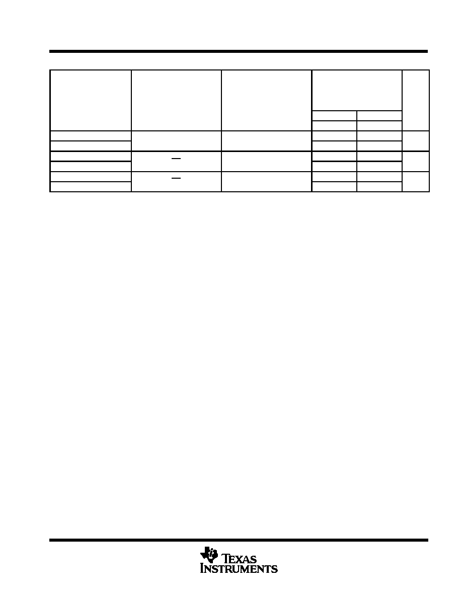
recommended operating conditions
SN54AS821A
SN74AS821A
UNIT
MIN
NOM
MAX
MIN
NOM
MAX
UNIT
VCC
Supply voltage
4.5
5
5.5
4.5
5
5.5
V
VIH
High-level input voltage
2
2
V
VIL
Low-level input voltage
0.8
0.8
V
IOH
High-level output current
� 24
� 24
mA
IOL
Low-level output current
32
48
mA
tw*
Pulse duration, CLK high or low
9
8
ns
tsu*
Setup time, data before CLK
7
6
ns
th*
Hold time, data after CLK
0
0
ns
TA
Operating free-air temperature
� 55
125
0
70
�
C
* On products compliant to MIL-STD-883, Class B, this parameter is based on characterization data but is not production tested.
electrical characteristics over recommended operating free-air temperature range (unless
otherwise noted)
PARAMETER
TEST CONDITIONS
SN54AS821A
SN74AS821A
UNIT
PARAMETER
TEST CONDITIONS
MIN
TYP
MAX
MIN
TYP
MAX
UNIT
VIK
VCC = 4.5 V,
II = � 18 mA
� 1.2
� 1.2
V
VCC = 4.5 V to 5.5 V,
IOH = � 2 mA
VCC � 2
VCC � 2
VOH
VCC = 4 5 V
IOH = � 15 mA
2.4
3.2
2.4
3.2
V
VCC = 4.5 V
IOH = � 24 mA
2
2
VOL
VCC = 4 5 V
IOL = 32 mA
0.25
0.5
V
VOL
VCC = 4.5 V
IOL = 48 mA
0.35
0.5
V
IOZH
VCC = 5.5 V,
VO = 2.7 V
50
50
�
A
IOZL
VCC = 5.5 V,
VI = 0.4 V
� 50
� 50
�
A
II
VCC = 5.5 V,
VI = 7 V
0.1
0.1
mA
IIH
VCC = 5.5 V,
VI = 2.7 V
20
20
�
A
IIL
VCC = 5.5 V,
VI = 0.4 V
� 0.5
� 0.5
mA
IO
VCC = 5.5 V,
VO = 2.25 V
� 30
� 112
� 30
� 112
mA
Outputs high
55
88
55
88
ICC
VCC = 5.5 V
Outputs low
68
109
68
109
mA
Outputs disabled
70
113
70
113
All typical values are at VCC = 5 V, TA = 25
�
C.
The output conditions have been chosen to produce a current that closely approximates one half of the true short-circuit output current, IOS.
SN54AS821A, SN74AS821A
10-BIT BUS-INTERFACE FLIP-FLOPS
WITH 3-STATE OUTPUTS
SDAS230A � DECEMBER 1983 � REVISED AUGUST 1995
4
POST OFFICE BOX 655303
�
DALLAS, TEXAS 75265
switching characteristics (see Figure 1)
PARAMETER
FROM
(INPUT)
TO
(OUTPUT)
VCC = 4.5 V to 5.5 V,
CL = 50 pF,
R1 = 500
,
R2 = 500
,
TA = MIN to MAX
UNIT
SN54AS821A
SN74AS821A
MIN
MAX
MIN
MAX
tPLH
CLK
An Q
3.5
9
3.5
7.5
ns
tPHL
CLK
Any Q
3.5
14
3.5
13
ns
tPZH
OE
An Q
4
12
3
11
ns
tPZL
OE
Any Q
4
13
4
12
ns
tPHZ
OE
Any Q
1
10
1
8
ns
tPLZ
OE
Any Q
1
10
1
8
ns
For conditions shown as MIN or MAX, use the appropriate value specified under recommended operating conditions.
SN54AS821A, SN74AS821A
10-BIT BUS-INTERFACE FLIP-FLOPS
WITH 3-STATE OUTPUTS
SDAS230A � DECEMBER 1983 � REVISED AUGUST 1995
5
POST OFFICE BOX 655303
�
DALLAS, TEXAS 75265
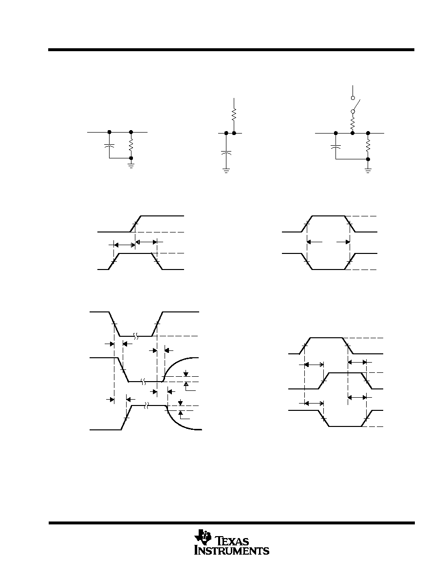
PARAMETER MEASUREMENT INFORMATION
SERIES 54ALS/ 74ALS AND 54AS/ 74AS DEVICES
tPHZ
tPLZ
tPHL
tPLH
0.3 V
tPZL
tPZH
tPLH
tPHL
LOAD CIRCUIT
FOR 3-STATE OUTPUTS
From Output
Under Test
Test
Point
R1
S1
CL
(see Note A)
7 V
1.3 V
1.3 V
1.3 V
3.5 V
3.5 V
0.3 V
0.3 V
th
tsu
VOLTAGE WAVEFORMS
SETUP AND HOLD TIMES
Timing
Input
Data
Input
1.3 V
1.3 V
3.5 V
3.5 V
0.3 V
0.3 V
High-Level
Pulse
Low-Level
Pulse
tw
VOLTAGE WAVEFORMS
PULSE DURATIONS
Input
Out-of-Phase
Output
(see Note C)
1.3 V
1.3 V
1.3 V
1.3 V
1.3 V
1.3 V
1.3 V
1.3 V
1.3 V
1.3 V
3.5 V
3.5 V
0.3 V
0.3 V
VOL
VOH
VOH
VOL
Output
Control
(low-level
enabling)
Waveform 1
S1 Closed
(see Note B)
Waveform 2
S1 Open
(see Note B)
[
0 V
VOH
VOL
[
3.5 V
In-Phase
Output
0.3 V
1.3 V
1.3 V
VOLTAGE WAVEFORMS
PROPAGATION DELAY TIMES
VOLTAGE WAVEFORMS
ENABLE AND DISABLE TIMES, 3-STATE OUTPUTS
R2
VCC
RL
Test
Point
From Output
Under Test
CL
(see Note A)
LOAD CIRCUIT
FOR OPEN-COLLECTOR OUTPUTS
LOAD CIRCUIT FOR
BI-STATE
TOTEM-POLE OUTPUTS
From Output
Under Test
Test
Point
CL
(see Note A)
RL
RL = R1 = R2
NOTES: A. CL includes probe and jig capacitance.
B. Waveform 1 is for an output with internal conditions such that the output is low except when disabled by the output control.
Waveform 2 is for an output with internal conditions such that the output is high except when disabled by the output control.
C. When measuring propagation delay items of 3-state outputs, switch S1 is open.
D. All input pulses have the following characteristics: PRR
1 MHz, tr = tf = 2 ns, duty cycle = 50%.
E. The outputs are measured one at a time with one transition per measurement.
Figure 1. Load Circuits and Voltage Waveforms