TLC220x, TLC220xA, TLC220xB, TLC220xY
Advanced LinCMOS
TM
LOW-NOISE PRECISION
OPERATIONAL AMPLIFIERS
SLOS175 ≠ FEBRUARY 1997
1
POST OFFICE BOX 655303
∑
DALLAS, TEXAS 75265
D
B Grade Is 100% Tested for Noise
30 nV/
Hz Max at f = 10 Hz
12 nV/
Hz Max at f = 1 kHz
D
Low Input Offset Voltage . . . 500
µ
V Max
D
Excellent Offset Voltage Stability
With Temperature . . . 0.5
µ
V/
∞
C Typ
D
Rail-to-Rail Output Swing
D
Low Input Bias Current
1 pA Typ at T
A
= 25
∞
C
D
Common-Mode Input Voltage Range
Includes the Negative Rail
D
Fully Specified For Both Single-Supply and
Split-Supply Operation
description
The TLC220x, TLC220xA, TLC220xB, and
TLC220xY are precision, low-noise operational
amplifiers using Texas Instruments Advanced
LinCMOS
TM
process. These devices combine the
noise performance of the lowest-noise JFET
amplifiers with the dc precision available
previously only in bipolar amplifiers. The
Advanced LinCMOS
TM
process uses silicon-gate
technology to obtain input offset voltage stability
with temperature and time that far exceeds that
obtainable using metal-gate technology. In
addition, this technology makes possible input
impedance levels that meet or exceed levels
offered by top-gate JFET and expensive
dielectric-isolated devices.
The combination of excellent dc and noise
performance with a common-mode input voltage
range that includes the negative rail makes these
devices an ideal choice for high-impedance,
low-level signal-conditioning applications in either
single-supply or split-supply configurations.
The device inputs and outputs are designed to withstand ≠100-mA surge currents without sustaining latch-up.
In addition, internal ESD-protection circuits prevent functional failures at voltages up to 2000 V as tested under
MIL-PRF-38535, Method 3015.2; however, care should be exercised in handling these devices as exposure
to ESD may result in degradation of the parametric performance.
The C-suffix devices are characterized for operation from 0
∞
C to 70
∞
C. The I-suffix devices are characterized
for operation from ≠ 40
∞
C to 85
∞
C. The M-suffix devices are characterized for operation over the full military
temperature range of ≠ 55
∞
C to 125
∞
C.
Advanced LinCMOS is a trademark of Texas Instruments Incorporated.
Copyright
©
1997, Texas Instruments Incorporated
On products compliant to MIL-PRF-38535, all parameters are tested
unless otherwise noted. On all other products, production
processing does not necessarily include testing of all parameters.
PRODUCTION DATA information is current as of publication date.
Products conform to specifications per the terms of Texas Instruments
standard warranty. Production processing does not necessarily include
testing of all parameters.
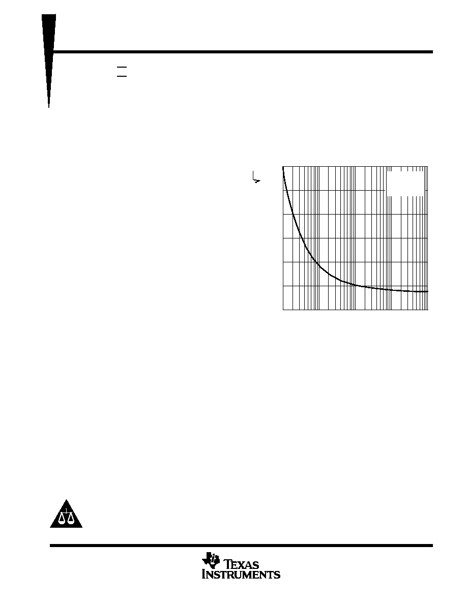
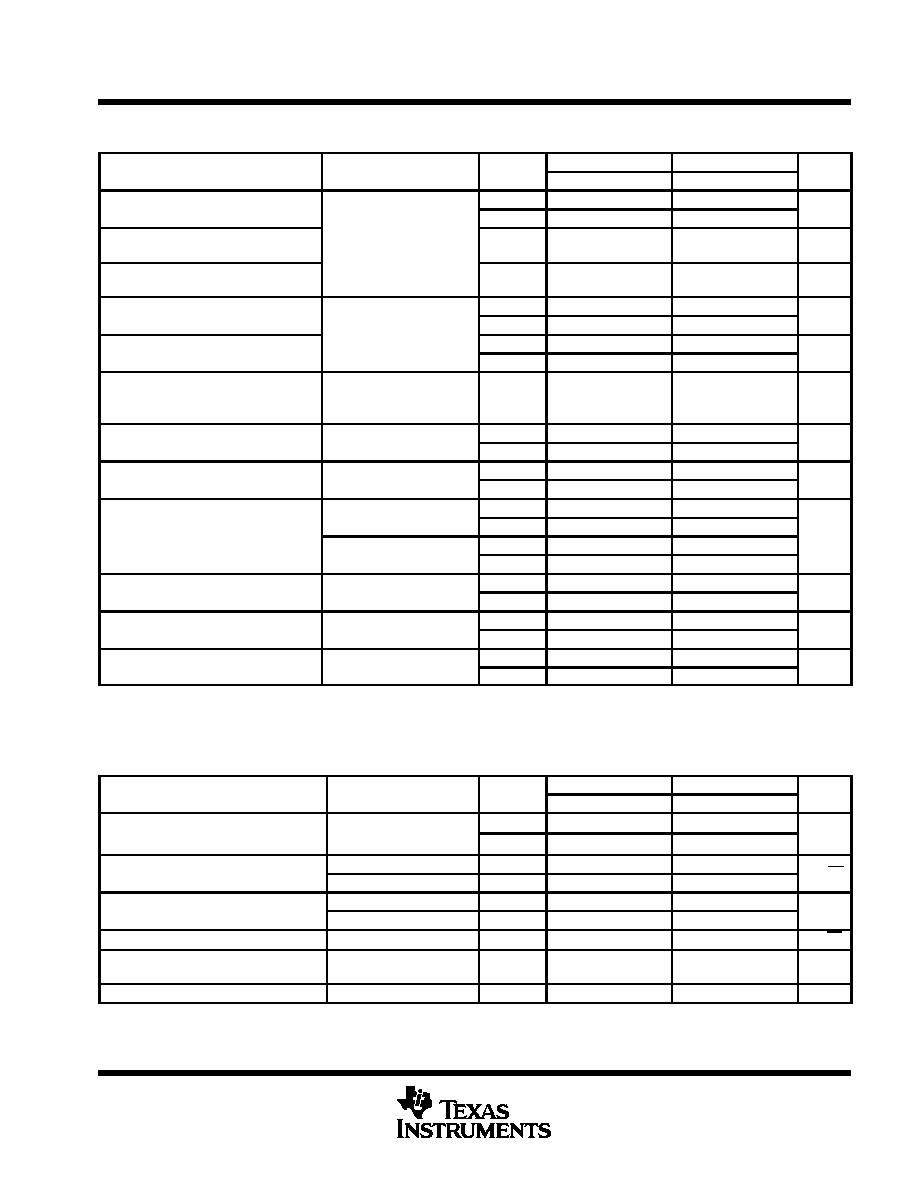
1
10
100
Vn ≠ Equivalent Input Noise V
oltage ≠ nV/ Hz
f ≠ Frequency ≠ Hz
TYPICAL EQUIVALENT
INPUT NOISE VOLTAGE
vs
FREQUENCY
60
1 k
10 k
50
40
30
20
10
0
VDD = 5 V
RS = 20
TA = 25
∞
C
Hz
V
n
Please be aware that an important notice concerning availability, standard warranty, and use in critical applications of
Texas Instruments semiconductor products and disclaimers thereto appears at the end of this data sheet.

TLC220x, TLC220xA, TLC220xB, TLC220xY
Advanced LinCMOS
TM
LOW-NOISE PRECISION
OPERATIONAL AMPLIFIERS
SLOS175 ≠ FEBRUARY 1997
2
POST OFFICE BOX 655303
∑
DALLAS, TEXAS 75265
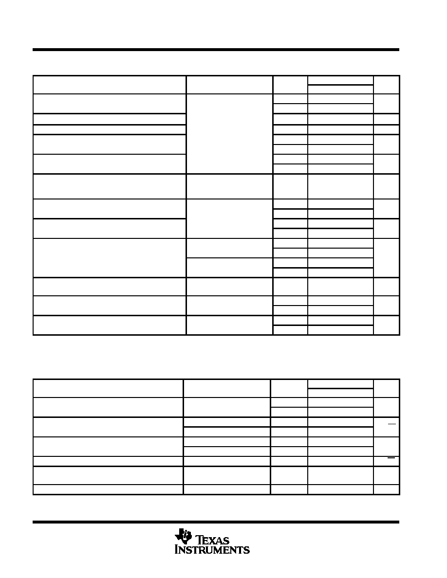
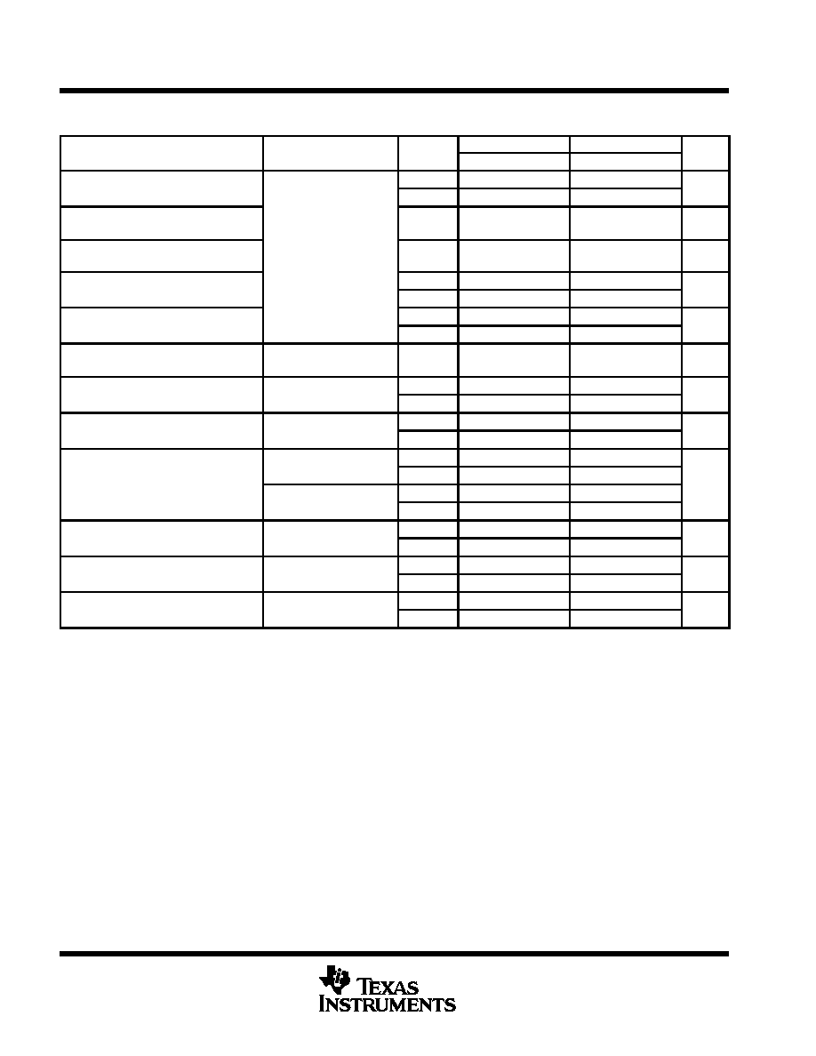
TLC2201 AVAILABLE OPTIONS
V max
V max
PACKAGED DEVICES
CHIP
TA
VIOmax
AT 25
∞
C
Vnmax
f = 10 Hz
AT 25
∞
C
Vnmax
f = 1 kHz
AT 25
∞
C
SMALL
OUTLINE
(D)
CHIP
CARRIER
(FK)
CERAMIC
DIP
(JG)
PLASTIC
DIP
(P)
CHIP
FORM
(Y)
0
∞
C
200
µ
V
35 nV/
Hz
15 nV/
Hz
TLC2201ACD
TLC2201ACP
0 C
to
200
µ
V
200
µ
V
35 nV/
Hz
30 nV/
Hz
15 nV/
Hz
12 nV/
Hz
TLC2201ACD
TLC2201BCD
--
--
TLC2201ACP
TLC2201BCP
TLC2201Y
70
∞
C
µ
500
µ
V
--
--
TLC2201CD
TLC2201CP
≠ 40
∞
C
200
µ
V
35 nV/
Hz
15 nV/
Hz
TLC2201AID
TLC2201AIP
40 C
to
200
µ
V
200
µ
V
35 nV/
Hz
30 nV/
Hz
15 nV/
Hz
12 nV/
Hz
TLC2201AID
TLC2201BID
--
--
TLC2201AIP
TLC2201BIP
--
85
∞
C
µ
500
µ
V
--
--
TLC2201ID
TLC2201IP
≠ 55
∞
C
200
µ
V
35 nV/
Hz
15 nV/
Hz
TLC2201AMD
TLC2201AMFK
TLC2201AMJG
TLC2201AMP
to
µ
200
µ
V
35 nV/
Hz
30 nV/
Hz
15 nV/
Hz
12 nV/
Hz
TLC2201BMD
TLC2201BMFK
TLC2201BMJG
TLC2201BMP
--
125
∞
C
500
µ
V
--
--
TLC2201MD
TLC2201MFK
TLC2201MJG
TLC2201MP
The D packages are available taped and reeled. Add R suffix to device type (e.g. TLC220xBCDR).
Chip forms are tested at 25
∞
C only.
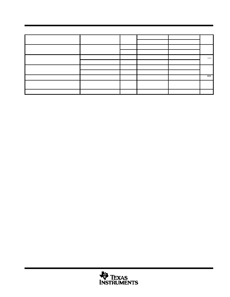
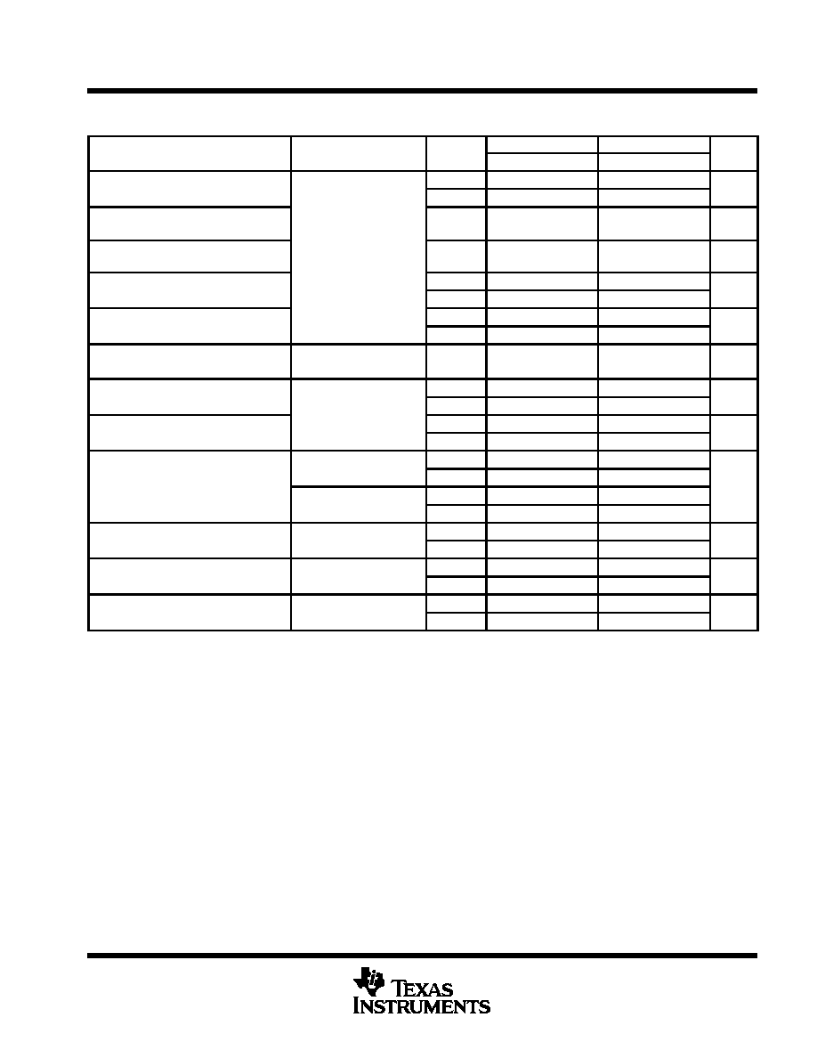
TLC2202 AVAILABLE OPTIONS
V max
V max
PACKAGED DEVICES
CHIP
TA
VIOmax
AT 25
∞
C
Vnmax
f = 10 Hz
AT 25
∞
C
Vnmax
f = 1 kHz
AT 25
∞
C
SMALL
OUTLINE
(D)
CHIP
CARRIER
(FK)
CERAMIC
DIP
(JG)
PLASTIC
DIP
(P)
CHIP
FORM
(Y)
500
µ
V
30 nV/
Hz
12 nV/
Hz
TLC2202BCD
--
--
TLC2202BCP
0
∞
C to 70
∞
C
500
µ
V
500
µ
V
30 nV/
Hz
35 nV/
Hz
12 nV/
Hz
15 nV/
Hz
TLC2202BCD
TLC2202ACD
--
--
TLC2202BCP
TLC2202ACP
TLC2202Y
1 mV
--
--
TLC2202CD
--
--
TLC2202CP
500
µ
V
30 nV/
Hz
12 nV/
Hz
TLC2202BID
--
--
TLC2202BIP
≠ 40
∞
C to 85
∞
C
500
µ
V
500
µ
V
30 nV/
Hz
35 nV/
Hz
12 nV/
Hz
15 nV/
Hz
TLC2202BID
TLC2202AID
--
--
TLC2202BIP
TLC2202AIP
--
1 mV
--
--
TLC2202ID
--
--
TLC2202IP
500
µ
V
30 nV/
Hz
12 nV/
Hz
TLC2202BMD
TLC2202BMFK
TLC2202BMJG
TLC2202BMP
≠ 55
∞
C to 125
∞
C
500
µ
V
500
µ
V
30 nV/
Hz
35 nV/
Hz
12 nV/
Hz
15 nV/
Hz
TLC2202BMD
TLC2202AMD
TLC2202BMFK
TLC2202AMFK
TLC2202BMJG
TLC2202AMJG
TLC2202BMP
TLC2202AMP
--
1 mV
--
--
TLC2202MD
TLC2202MFK
TLC2202MJG
TLC2202MP
The D packages are available taped and reeled. Add R suffix to device type (e.g. TLC220xBCDR).
Chip forms are tested at 25
∞
C only.
TLC220x, TLC220xA, TLC220xB, TLC220xY
Advanced LinCMOS
TM
LOW-NOISE PRECISION
OPERATIONAL AMPLIFIERS
SLOS175 ≠ FEBRUARY 1997
3
POST OFFICE BOX 655303
∑
DALLAS, TEXAS 75265
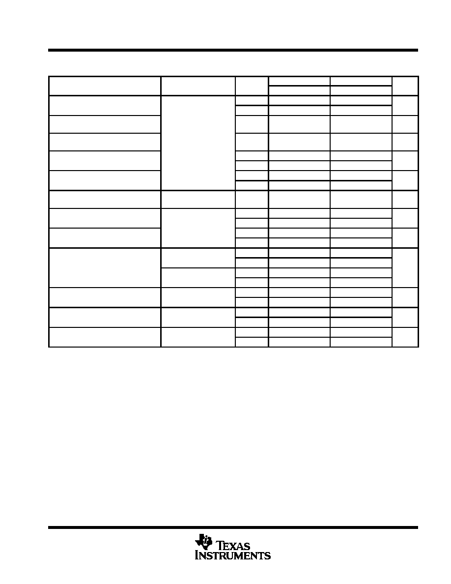
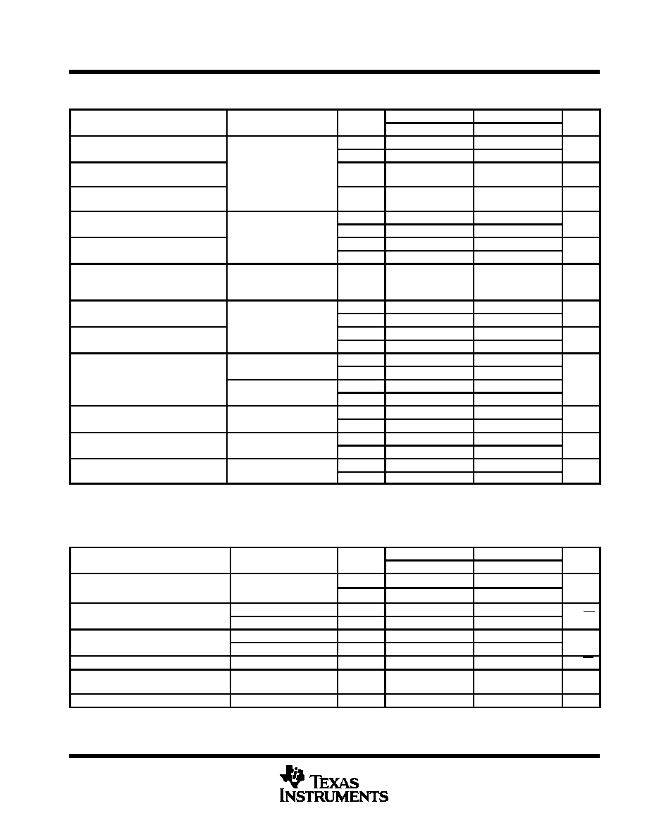
1
2
3
4
5
6
7
14
13
12
11
10
9
8
NC
NC
1OUT
1IN ≠
1IN +
V
DD ≠
/GND
NC
NC
NC
V
DD +
2OUT
2IN ≠
2IN +
NC
1
2
3
4
8
7
6
5
1OUT
1IN ≠
1IN +
V
DD ≠
/GND
V
DD +
2OUT
2IN ≠
2IN +
NC ≠ No internal connection
3
2
1 20 19
9 10 11 12 13
4
5
6
7
8
18
17
16
15
14
NC
2OUT
NC
2IN ≠
NC
NC
1IN ≠
NC
1IN +
NC
NC
1OUT
NC
NC
NC
NC
NC
2IN+
DD+
V
DD ≠
V
/GND
1
2
3
4
8
7
6
5
NC
IN ≠
IN +
V
DD ≠
/GND
NC
V
DD +
OUT
NC
3
2
1 20 19
9 10 11 12 13
4
5
6
7
8
18
17
16
15
14
NC
V
DD +
NC
OUT
NC
NC
IN ≠
NC
IN +
NC
NC
NC
NC
NC
NC
NC
NC
DD ≠
V
NC
NC
/GND
TLC2201
FK PACKAGE
(TOP VIEW)
TLC2202
D PACKAGE
(TOP VIEW)
TLC2202
JG OR P PACKAGE
(TOP VIEW)
TLC2202
FK PACKAGE
(TOP VIEW)
TLC2201
D, JG, OR P PACKAGE
(TOP VIEW)

TLC220x, TLC220xA, TLC220xB, TLC220xY
Advanced LinCMOS
TM
LOW-NOISE PRECISION
OPERATIONAL AMPLIFIERS
SLOS175 ≠ FEBRUARY 1997
4
POST OFFICE BOX 655303
∑
DALLAS, TEXAS 75265
equivalent schematic (each amplifier)
IN +
IN ≠
Q3
Q6
Q9
Q12
Q14
Q16
Q13
Q15
Q17
Q7
Q8
Q10
Q11
Q2
Q5
Q1
Q4
R1
R2
D1
C1
VDD +
VDD ≠ / GND
OUT
ACTUAL DEVICE COMPONENT COUNT
COMPONENT
TLC2201
TLC2202
Transistors
17
34
Resistors
2
2
Diodes
1
4
Capacitors
1
2
TLC220x, TLC220xA, TLC220xB, TLC220xY
Advanced LinCMOS
TM
LOW-NOISE PRECISION
OPERATIONAL AMPLIFIERS
SLOS175 ≠ FEBRUARY 1997
5
POST OFFICE BOX 655303
∑
DALLAS, TEXAS 75265
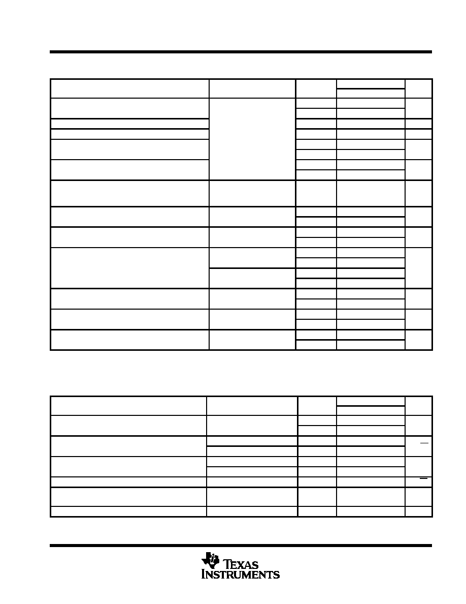
TLC2201Y chip information
This chip, when properly assembled, displays characteristics similar to the TLC2201C. Thermal compression
or ultrasonic bonding may be used on the doped-aluminum bonding path. Chips may be mounted with
conductive epoxy or a gold-silicon preform.
BONDING PAD ASSIGNMENTS
CHIP THICKNESS: 15 MILS TYPICAL
BONDING PADS: 4
◊
4 MILS MINIMUM
TJmax = 150
∞
C
TOLERANCES ARE
±
10%.
ALL DIMENSIONS ARE IN MILS.
PIN (4) IS INTERNALLY CONNECTED
TO BACK SIDE OF CHIP.
TERMINAL NUMBERS ARE FOR THE
D, JG, AND P PACKAGES.
+
≠
OUT
IN ≠
IN +
VDD+
(7)
(2)
(3)
(6)
(4)
VDD ≠
65
77
(2)
(3)
(4)
(6)
(7)
(8)
(1)
TLC220x, TLC220xA, TLC220xB, TLC220xY
Advanced LinCMOS
TM
LOW-NOISE PRECISION
OPERATIONAL AMPLIFIERS
SLOS175 ≠ FEBRUARY 1997
6
POST OFFICE BOX 655303
∑
DALLAS, TEXAS 75265
TLC2202Y chip formation
This chip, when properly assembled, displays characteristics similar to the TLC2202C. Thermal compression
or ultrasonic bonding may be used on the doped-aluminum bonding pads. Chips may be mounted with
conductive epoxy or a gold-silicon preform.
BONDING PAD ASSIGNMENTS
CHIP THICKNESS: 15 MILS TYPICAL
BONDING PADS: 4
◊
4 MILS MINIMUM
TJmax = 150
∞
C
TOLERANCES ARE
±
10%.
ALL DIMENSIONS ARE IN MILS.
PIN (4) IS INTERNALLY CONNECTED
TO BACKSIDE OF CHIP.
+
≠
1OUT
1IN +
1IN ≠
VDD+
(8)
(6)
(3)
(2)
(5)
(1)
≠
+
(7)
2IN +
2IN ≠
2OUT
(4)
VDD≠
100
80
(1)
(2)
(3)
(4)
(5)
(6)
(7)
(8)

TLC220x, TLC220xA, TLC220xB, TLC220xY
Advanced LinCMOS
TM
LOW-NOISE PRECISION
OPERATIONAL AMPLIFIERS
SLOS175 ≠ FEBRUARY 1997
7
POST OFFICE BOX 655303
∑
DALLAS, TEXAS 75265
absolute maximum ratings over operating free-air temperature range (unless otherwise noted)
Supply voltage, V
DD +
(see Note 1)
8 V
. . . . . . . . . . . . . . . . . . . . . . . . . . . . . . . . . . . . . . . . . . . . . . . . . . . . . . . . . . . .
Supply voltage, V
DD ≠
≠ 8 V
. . . . . . . . . . . . . . . . . . . . . . . . . . . . . . . . . . . . . . . . . . . . . . . . . . . . . . . . . . . . . . . . . . . . . .
Differential input voltage, V
ID
(see Note 2)
±
16 V
. . . . . . . . . . . . . . . . . . . . . . . . . . . . . . . . . . . . . . . . . . . . . . . . . . .
Input voltage, V
I
(any input)
±
8 V
. . . . . . . . . . . . . . . . . . . . . . . . . . . . . . . . . . . . . . . . . . . . . . . . . . . . . . . . . . . . . . . . .
Input current, I
I
(each input)
±
5 mA
. . . . . . . . . . . . . . . . . . . . . . . . . . . . . . . . . . . . . . . . . . . . . . . . . . . . . . . . . . . . . . .
Output current, I
O
(each output)
±
50 mA
. . . . . . . . . . . . . . . . . . . . . . . . . . . . . . . . . . . . . . . . . . . . . . . . . . . . . . . . . .
Duration of short-circuit current at (or below) 25
∞
C (see Note 3)
unlimited
. . . . . . . . . . . . . . . . . . . . . . . . . . . . . .
Continuous total dissipation
See Dissipation Rating Table
. . . . . . . . . . . . . . . . . . . . . . . . . . . . . . . . . . . . . . . . . . .
Operating free-air temperature range, T
A
: C suffix
0
∞
C to 70
∞
C
. . . . . . . . . . . . . . . . . . . . . . . . . . . . . . . . . . . . . . .
I suffix
≠ 40
∞
C to 85
∞
C
. . . . . . . . . . . . . . . . . . . . . . . . . . . . . . . . . . . . . .
M suffix
≠ 55
∞
C to 125
∞
C
. . . . . . . . . . . . . . . . . . . . . . . . . . . . . . . . . . . .
Storage temperature range
≠ 65
∞
C to 150
∞
C
. . . . . . . . . . . . . . . . . . . . . . . . . . . . . . . . . . . . . . . . . . . . . . . . . . . . . . . .
Case temperature for 60 seconds: FK package
260
∞
C
. . . . . . . . . . . . . . . . . . . . . . . . . . . . . . . . . . . . . . . . . . . . . .
Lead temperature 1,6 mm (1/16 inch) from case for 10 seconds: D or P package
260
∞
C
. . . . . . . . . . . . . . . . .
Lead temperature 1,6 mm (1/16 inch) from case for 60 seconds: JG package
300
∞
C
. . . . . . . . . . . . . . . . . . . .
Stresses beyond those listed under "absolute maximum ratings" may cause permanent damage to the device. These are stress ratings only, and
functional operation of the device at these or any other conditions beyond those indicated under "recommended operating conditions" is not
implied. Exposure to absolute-maximum-rated conditions for extended periods may affect device reliability.
NOTES:
1. All voltage values except differential voltages are with respect to the midpoint between VDD + and VDD ≠ .
2. Differential voltages are at IN+ with respect to IN ≠.
3. The output may be shorted to either supply. Temperature and /or supply voltages must be limited to ensure that the maximum
dissipation rating in not exceeded.
DISSIPATION RATING TABLE
PACKAGE
TA
25
∞
C
DERATING FACTOR
TA = 70
∞
C
TA = 85
∞
C
TA = 125
∞
C
PACKAGE
A
POWER RATING
ABOVE TA = 25
∞
C
A
POWER RATING
A
POWER RATING
A
POWER RATING
D≠8
725 mW
5.8 mW/
∞
C
464 mW
377 mW
145 mW
D≠14
950 mW
7.6 mW/
∞
C
608 mW
494 mW
190 mW
FK
1375 mW
11.0 mW/
∞
C
880 mW
715 mW
275 mW
JG
1050 mW
8.4 mW/
∞
C
672 mW
546 mW
210 mW
P
1000 mW
8.0 mW/
∞
C
640 mW
520 mW
200 mW
recommended operating conditions
C SUFFIX
I SUFFIX
M SUFFIX
UNIT
MIN
MAX
MIN
MAX
MIN
MAX
UNIT
Supply voltage, VDD
±
±
2.3
±
8
±
2.3
±
8
±
2.3
±
8
V
Common-mode input voltage, VIC
VDD ≠ VDD + ≠ 2.3
VDD ≠ VDD + ≠ 2.3
VDD ≠ VDD + ≠ 2.3
V
Operating free-air temperature, TA
0
70
≠ 40
85
≠ 55
125
∞
C
TLC220x, TLC220xA, TLC220xB, TLC220xY
Advanced LinCMOS
TM
LOW-NOISE PRECISION
OPERATIONAL AMPLIFIERS
SLOS175 ≠ FEBRUARY 1997
8
POST OFFICE BOX 655303
∑
DALLAS, TEXAS 75265
TLC2201C electrical characteristics at specified free-air temperature, V
DD
±
=
±
5 V (unless
otherwise noted)
PARAMETER
TEST CONDITIONS
TA
TLC2201C
UNIT
PARAMETER
TEST CONDITIONS
TA
MIN
TYP
MAX
UNIT
VIO
Input offset voltage
25
∞
C
100
500
µ
V
VIO
Input offset voltage
Full range
600
µ
V
VIO
Temperature coefficient of input offset voltage
Full range
0 5
µ
V/
∞
C
VIO
Temperature coefficient of input offset voltage
Full range
0.5
µ
V/
∞
C
Input offset voltage long-term drift (see Note 4)
VIC = 0
RS = 50
25
∞
C
0.001
0.005
µ
V/mo
IIO
Input offset current
VIC = 0,
RS = 50
25
∞
C
0.5
pA
IIO
Input offset current
Full range
100
pA
IIB
Input bias current
25
∞
C
1
pA
IIB
Input bias current
Full range
100
pA
≠ 5
VICR
Common-mode input voltage range
RS = 50
Full range
5
to
V
ICR
g
g
S
g
2.7
VOM
Maximum positive peak output voltage swing
25
∞
C
4.7
4.8
V
VOM + Maximum positive peak output voltage swing
RL = 10 k
Full range
4.7
V
VOM
Maximum negative peak output voltage swing
RL = 10 k
25
∞
C
≠ 4.7
≠ 4.9
V
VOM ≠ Maximum negative peak output voltage swing
Full range
≠ 4.7
V
VO =
±
4 V
RL = 500 k
25
∞
C
400
560
AVD
Large signal differential voltage amplification
VO =
±
4 V,
RL = 500 k
Full range
300
V/mV
AVD
Large-signal differential voltage amplification
VO =
±
4 V
RL = 10 k
25
∞
C
90
100
V/mV
VO =
±
4 V,
RL = 10 k
Full range
70
CMRR
Common mode rejection ratio
VIC = VICRmin, VO = 0,
Full range
85
dB
CMRR
Common-mode rejection ratio
IC
ICR
,
RS = 50
O
,
Full range
85
dB
kSVR
Supply voltage rejection ratio (
VDD
±
/
VIO)
VDD
±
=
±
2 3 V to
±
8 V
25
∞
C
90
110
dB
kSVR
Supply voltage rejection ratio (
VDD
±
/
VIO)
VDD
±
=
±
2.3 V to
±
8 V
Full range
85
dB
IDD
Supply current
VO = 0
No load
25
∞
C
1.1
1.5
mA
IDD
Supply current
VO = 0,
No load
Full range
1.5
mA
Full range is 0
∞
C to 70
∞
C.
NOTE 4: Typical values are based on the input offset voltage shift observed through 168 hours of operating life test at TA = 150
∞
C extrapolated
to TA = 25
∞
C using the Arrhenius equation and assuming an activation energy of 0.96 eV.
TLC2201C operating characteristics at specified free-air temperature, V
DD
±
=
±
5 V
PARAMETER
TEST CONDITIONS
TA
TLC2201C
UNIT
PARAMETER
TEST CONDITIONS
TA
MIN
TYP
MAX
UNIT
SR
Slew rate at unity gain
VO =
±
2.3 V,
RL = 10 k
,
25
∞
C
2
2.7
V/
µ
s
SR
Slew rate at unity gain
CL = 100 pF
Full range
1.5
V/
µ
s
V
Equivalent input noise voltage
f = 10 Hz
25
∞
C
18
nV/
Hz
Vn
Equivalent input noise voltage
f = 1 kHz
25
∞
C
8
nV/
Hz
VN(PP)
Peak to peak equivalent input noise voltage
f = 0.1 to 1 Hz
25
∞
C
0.5
µ
V
VN(PP)
Peak-to-peak equivalent input noise voltage
f = 0.1 to 10 Hz
25
∞
C
0.7
µ
V
In
Equivalent input noise current
25
∞
C
0.6
fA/
Hz
Gain bandwidth product
f = 10 kHz,
RL = 10 k
,
25
∞
C
1 9
MHz
Gain-bandwidth product
CL = 100 pF
L
25
∞
C
1.9
MHz
m
Phase margin at unity gain
RL = 10 k
,
CL = 100 pF
25
∞
C
48
∞
Full range is 0
∞
C to 70
∞
C.
TLC220x, TLC220xA, TLC220xB, TLC220xY
Advanced LinCMOS
TM
LOW-NOISE PRECISION
OPERATIONAL AMPLIFIERS
SLOS175 ≠ FEBRUARY 1997
9
POST OFFICE BOX 655303
∑
DALLAS, TEXAS 75265
TLC2201C electrical characteristics at specified free-air temperature, V
DD
±
=
±
5 V (unless
otherwise noted)
PARAMETER
TEST CONDITIONS
TA
TLC2201AC
TLC2201BC
UNIT
PARAMETER
TEST CONDITIONS
TA
MIN
TYP
MAX
MIN
TYP
MAX
UNIT
VIO
Input offset voltage
25
∞
C
80
200
80
200
µ
V
VIO
Input offset voltage
Full range
300
300
µ
V
VIO
Temperature coefficient of input
offset voltage
Full range
0.5
0.5
µ
V/
∞
C
Input offset voltage long-term
drift (see Note 4)
VIC = 0,
RS = 50
25
∞
C
0.001
0.005
0.001
0.005
µ
V/mo
IIO
Input offset current
25
∞
C
0.5
0.5
pA
IIO
Input offset current
Full range
100
100
pA
IIB
Input bias current
25
∞
C
1
1
pA
IIB
Input bias current
Full range
100
100
pA
VICR
Common-mode input voltage
range
RS = 50
Full range
≠ 5 to
2.7
≠ 5 to
2.7
V
VOM
Maximum positive peak output
25
∞
C
4.7
4.8
4.7
4.8
V
VOM +
voltage swing
RL = 10 k
Full range
4.7
4.7
V
VOM
Maximum negative peak output
RL = 10 k
25
∞
C
≠ 4.7
≠ 4.9
≠ 4.7
≠ 4.9
V
VOM ≠
g
voltage swing
Full range
≠ 4.7
≠ 4.7
V
VO =
±
4 V
RL = 500 k
25
∞
C
400
560
400
560
AVD
Large-signal differential voltage
VO =
±
4 V,
RL = 500 k
Full range
300
300
V/mV
AVD
g
g
g
amplification
VO =
±
4 V
RL = 10 k
25
∞
C
90
100
90
100
V/mV
VO =
±
4 V,
RL = 10 k
Full range
70
70
CMRR
Common mode rejection ratio
VIC = VICRmin,
25
∞
C
90
115
90
115
dB
CMRR
Common-mode rejection ratio
VO = 0,
RS = 50
Full range
85
85
dB
kSVR
Supply voltage rejection ratio
VDD
±
=
±
2 3 V to
±
8 V
25
∞
C
90
110
90
110
dB
kSVR
y
g
j
(
VDD
±
/
VIO)
VDD
±
=
±
2.3 V to
±
8 V
Full range
85
85
dB
IDD
Supply current
VO = 0
No load
25
∞
C
1.1
1.5
1.1
1.5
mA
IDD
Supply current
VO = 0,
No load
Full range
1.5
1.5
mA
Full range is 0
∞
C to 70
∞
C.
NOTE 4: Typical values are based on the input offset voltage shift observed through 168 hours of operating life test at TA = 150
∞
C extrapolated
to TA = 25
∞
C using the Arrhenius equation and assuming an activation energy of 0.96 eV.
TLC220x, TLC220xA, TLC220xB, TLC220xY
Advanced LinCMOS
TM
LOW-NOISE PRECISION
OPERATIONAL AMPLIFIERS
SLOS175 ≠ FEBRUARY 1997
10
POST OFFICE BOX 655303
∑
DALLAS, TEXAS 75265
TLC2201C operating characteristics at specified free-air temperature, V
DD
±
=
±
5 V
PARAMETER
TEST CONDITIONS
TA
TLC2201AC
TLC2210BC
UNIT
PARAMETER
TEST CONDITIONS
TA
MIN
TYP
MAX
MIN
TYP
MAX
UNIT
SR
Slew rate at unity gain
VO =
±
2.3 V,
RL = 10 k
,
25
∞
C
2
2.7
2
2.7
V/
µ
s
SR
Slew rate at unity gain
O
,
CL = 100 pF
Full range
1.5
1.5
V/
µ
s
V
Equivalent input noise volt-
f = 10 Hz
25
∞
C
18
35
18
30
nV/
Hz
Vn
q
age (see Note 5)
f = 1 kHz
25
∞
C
8
15
8
12
nV/
Hz
VN(PP)
Peak-to-peak equivalent input
f = 0.1 to 1 Hz
25
∞
C
0.5
0.5
µ
V
VN(PP)
q
noise voltage
f = 0.1 to 10 Hz
25
∞
C
0.7
0.7
µ
V
In
Equivalent input noise current
25
∞
C
0.6
0.6
fA/
Hz
Gain bandwidth product
f = 10 kHz,
RL = 10 k
,
25
∞
C
1 9
1 9
MHz
Gain-bandwidth product
,
CL = 100 pF
L
25
∞
C
1.9
1.9
MHz
m
Phase margin at unity gain
RL = 10 k
,
CL = 100 pF
25
∞
C
48
∞
48
∞
Full range is 0
∞
C to 70
∞
C.
NOTE 5: This parameter is tested on a sample basis for the TLC2201A and on all devices for the TLC2201B. For other test requirements, please
contact the factory. This statement has no bearing on testing or nontesting of other parameters.
TLC220x, TLC220xA, TLC220xB, TLC220xY
Advanced LinCMOS
TM
LOW-NOISE PRECISION
OPERATIONAL AMPLIFIERS
SLOS175 ≠ FEBRUARY 1997
11
POST OFFICE BOX 655303
∑
DALLAS, TEXAS 75265
TLC2201C electrical characteristics at specified free-air temperature, V
DD
= 5 V (unless otherwise
noted)
PARAMETER
TEST CONDITIONS
TA
TLC2201C
UNIT
PARAMETER
TEST CONDITIONS
TA
MIN
TYP
MAX
UNIT
VIO
Input offset voltage
25
∞
C
100
500
µ
V
VIO
Input offset voltage
Full range
600
µ
V
VIO
Temperature coefficient of input offset voltage
Full range
0.5
µ
V/
∞
C
Input offset voltage long-term drift (see Note 4)
VIC = 0
RS = 50
25
∞
C
0.001
0.005
µ
V/mo
IIO
Input offset current
VIC = 0,
RS = 50
25
∞
C
0.5
pA
IIO
Input offset current
Full range
100
pA
IIB
Input bias current
25
∞
C
1
pA
IIB
Input bias current
Full range
100
pA
0
VICR
Common-mode input voltage range
RS = 50
Full range
0
to
V
ICR
g
g
S
g
2.7
VOH
Maximum high level output voltage
RL = 10 k
25
∞
C
4.7
4.8
V
VOH
Maximum high-level output voltage
RL = 10 k
Full range
4.7
V
VOL
Maximum low level output voltage
IO = 0
25
∞
C
0
50
mV
VOL
Maximum low-level output voltage
IO = 0
Full range
50
mV
VO = 1 V to 4 V,
25
∞
C
150
315
AVD
Large signal differential voltage amplification
O
,
RL = 500 k
Full range
100
V/mV
AVD
Large-signal differential voltage amplification
VO = 1 V to 4 V,
25
∞
C
25
55
V/mV
O
,
RL = 10 k
Full range
15
CMRR
Common mode rejection ratio
VIC = VICRmin, VO = 0,
25
∞
C
90
110
dB
CMRR
Common-mode rejection ratio
IC
ICR
,
RS = 50
O
,
Full range
85
dB
kSVR
Supply voltage rejection ratio (
VDD
±
/
VIO)
VDD = 4 6 V to 16 V
25
∞
C
90
110
dB
kSVR
Supply voltage rejection ratio (
VDD
±
/
VIO)
VDD = 4.6 V to 16 V
Full range
85
dB
IDD
Supply current
VO = 2 5 V
No load
25
∞
C
1
1.5
mA
IDD
Supply current
VO = 2.5 V,
No load
Full range
1.5
mA
Full range is 0
∞
C to 70
∞
C.
NOTE 4: Typical values are based on the input offset voltage shift observed through 168 hours of operating life test at TA = 150
∞
C extrapolated
to TA = 25
∞
C using the Arrhenius equation and assuming an activation energy of 0.96 eV.
TLC2201C operating characteristics at specified free-air temperature, V
DD
= 5 V
PARAMETER
TEST CONDITIONS
TA
TLC2201C
UNIT
PARAMETER
TEST CONDITIONS
TA
MIN
TYP
MAX
UNIT
SR
Slew rate at unity gain
VO = 0.5 V to 2.5 V,
25
∞
C
1.8
2.5
V/
µ
s
SR
Slew rate at unity gain
RL = 10 k
,
CL = 100 pF
Full range
1.3
V/
µ
s
V
Equivalent input noise voltage
f = 10 Hz
25
∞
C
18
nV/
Hz
Vn
Equivalent input noise voltage
f = 1 kHz
25
∞
C
8
nV/
Hz
VN(PP)
Peak to peak equivalent input noise voltage
f = 0.1 to 1 Hz
25
∞
C
0.5
µ
V
VN(PP)
Peak-to-peak equivalent input noise voltage
f = 0.1 to 10 Hz
25
∞
C
0.7
µ
V
In
Equivalent input noise current
25
∞
C
0.6
fA/
Hz
Gain bandwidth product
f = 10 kHz,
RL = 10 k
,
25
∞
C
1 8
MHz
Gain-bandwidth product
CL = 100 pF
L
25
∞
C
1.8
MHz
m
Phase margin at unity gain
RL = 10 k
,
CL = 100 pF
25
∞
C
45
∞
Full range is 0
∞
C to 70
∞
C.
TLC220x, TLC220xA, TLC220xB, TLC220xY
Advanced LinCMOS
TM
LOW-NOISE PRECISION
OPERATIONAL AMPLIFIERS
SLOS175 ≠ FEBRUARY 1997
12
POST OFFICE BOX 655303
∑
DALLAS, TEXAS 75265
TLC2201C electrical characteristics at specified free-air temperature, V
DD
= 5 V (unless otherwise
noted)
PARAMETER
TEST CONDITIONS
TA
TLC2201AC
TLC2201BC
UNIT
PARAMETER
TEST CONDITIONS
TA
MIN
TYP
MAX
MIN
TYP
MAX
UNIT
VIO
Input offset voltage
25
∞
C
80
200
80
200
µ
V
VIO
Input offset voltage
Full range
300
300
µ
V
VIO
Temperature coefficient of
Full range
0 5
0 5
µ
V/
∞
C
VIO
input offset voltage
Full range
0.5
0.5
µ
V/
∞
C
Input offset voltage long-term
drift (see Note 4)
VIC = 0,
RS = 50
25
∞
C
0.001
0.005
0.001
0.005
µ
V/mo
IIO
Input offset current
25
∞
C
0.5
0.5
pA
IIO
Input offset current
Full range
100
100
pA
IIB
Input bias current
25
∞
C
1
1
pA
IIB
Input bias current
Full range
100
100
pA
VICR
Common-mode input voltage
RS = 50
Full range
0 to
0 to
V
VICR
g
range
RS = 50
Full range
2.7
2.7
V
VOH
Maximum high-level output
RL = 10 k
25
∞
C
4.7
4.8
4.7
4.8
V
VOH
g
voltage
RL = 10 k
Full range
4.7
4.7
V
VOL
Maximum low-level output
IO = 0
25
∞
C
0
50
0
50
mV
VOL
voltage
IO = 0
Full range
50
50
mV
VO = 1 V to 4 V,
25
∞
C
150
315
150
315
AVD
Large-signal differential
O
,
RL = 500 k
Full range
100
100
V/mV
AVD
g
g
voltage amplification
VO = 1 V to 4 V,
25
∞
C
25
55
25
55
V/mV
O
,
RL = 10 k
Full range
15
15
CMRR
Common mode rejection ratio
VIC = VICRmin,
25
∞
C
90
110
90
110
dB
CMRR
Common-mode rejection ratio
VO = 0,
RS = 50
Full range
85
85
dB
kSVR
Supply voltage rejection ratio
VDD = 4 6 V to 16 V
25
∞
C
90
110
90
110
dB
kSVR
y
g
j
(
VDD
±
/
VIO)
VDD = 4.6 V to 16 V
Full range
85
85
dB
IDD
Supply current
VO = 2 5 V
No load
25
∞
C
1
1.5
1
1.5
mA
IDD
Supply current
VO = 2.5 V,
No load
Full range
1.5
1.5
mA
Full range is 0
∞
C to 70
∞
C.
NOTE 4: Typical values are based on the input offset voltage shift observed through 168 hours of operating life test at TA = 150
∞
C extrapolated
to TA = 25
∞
C using the Arrhenius equation and assuming an activation energy of 0.96 eV.
TLC220x, TLC220xA, TLC220xB, TLC220xY
Advanced LinCMOS
TM
LOW-NOISE PRECISION
OPERATIONAL AMPLIFIERS
SLOS175 ≠ FEBRUARY 1997
13
POST OFFICE BOX 655303
∑
DALLAS, TEXAS 75265
TLC2201C operating characteristics at specified free-air temperature, V
DD
= 5 V
PARAMETER
TEST CONDITIONS
TA
TLC2201AC
TLC2210BC
UNIT
PARAMETER
TEST CONDITIONS
TA
MIN
TYP
MAX
MIN
TYP
MAX
UNIT
SR
Slew rate at unity gain
VO = 0.5 V to 2.5 V,
25
∞
C
1.8
2.5
1.8
2.5
V/
µ
s
SR
Slew rate at unity gain
RL = 10 k
,
CL = 100 pF
Full range
1.3
1.3
V/
µ
s
V
Equivalent input noise voltage
f = 10 Hz
25
∞
C
18
35
18
30
nV/
Hz
Vn
q
g
(see Note 5)
f = 1 kHz
25
∞
C
8
15
8
12
nV/
Hz
VN(PP)
Peak-to-peak equivalent input
f = 0.1 to 1 Hz
25
∞
C
0.5
0.5
µ
V
VN(PP)
q
noise voltage
f = 0.1 to 10 Hz
25
∞
C
0.7
0.7
µ
V
In
Equivalent input noise current
25
∞
C
0.6
0.6
fA/
Hz
Gain-bandwidth product
f = 10 kHz,
CL = 100 pF
RL = 10 k
,
25
∞
C
1.8
1.8
MHz
m
Phase margin at unity gain
RL = 10 k
,
CL = 100 pF
25
∞
C
45
∞
45
∞
Full range is 0
∞
C to 70
∞
C.
NOTE 5: This parameter is tested on a sample basis for the TLC2201A and on all devices for the TLC2201B. For other test requirements, please
contact the factory. This statement has no bearing on testing or nontesting of other parameters.

TLC220x, TLC220xA, TLC220xB, TLC220xY
Advanced LinCMOS
TM
LOW-NOISE PRECISION
OPERATIONAL AMPLIFIERS
SLOS175 ≠ FEBRUARY 1997
14
POST OFFICE BOX 655303
∑
DALLAS, TEXAS 75265
TLC2202C electrical characteristics at specified free-air temperature, V
DD
±
=
±
5 V (unless
otherwise specified)
PARAMETER
TEST CONDITIONS
TA
TLC2202C
UNIT
PARAMETER
TEST CONDITIONS
TA
MIN
TYP
MAX
UNIT
VIO
Input offset voltage
25
∞
C
100
1000
µ
V
VIO
Input offset voltage
VIC = 0
RS = 50
Full range
1150
µ
V
VIO
Temperature coefficient of input offset voltage
VIC = 0,
RS = 50
Full range
0.5
µ
V/
∞
C
Input offset voltage long-term drift (see Note 4)
25
∞
C
0.001
0.005
µ
V/mo
IIO
Input offset current
25
∞
C
0.5
IIO
Input offset current
VIC = 0
RS = 50
Full range
100
pA
IIB
Input bias current
VIC = 0,
RS = 50
25
∞
C
1
pA
IIB
Input bias current
Full range
100
≠ 5
VICR
Common-mode input voltage range
RS = 50
Full range
5
to
V
ICR
g
g
S
g
2.7
VOM
Maximum positive peak output voltage swing
25
∞
C
4.7
4.8
VOM + Maximum positive peak output voltage swing
RL = 10 k
Full range
4.7
V
VOM
Maximum negative peak output voltage swing
RL = 10 k
25
∞
C
≠ 4.7
≠ 4.9
VOM ≠ Maximum negative peak output voltage swing
Full range
≠ 4.7
V
VO =
±
4 V
RL = 500 k
25
∞
C
300
560
AVD
Large signal differential voltage amplification
VO =
±
4 V,
RL = 500 k
Full range
200
V/mV
AVD
Large-signal differential voltage amplification
VO =
±
4 V
RL = 10 k
25
∞
C
50
100
V/mV
VO =
±
4 V,
RL = 10 k
Full range
25
CMRR
Common mode rejection ratio
VO = 0,
VIC = VICRmin,
25
∞
C
80
115
dB
CMRR
Common-mode rejection ratio
O
,
IC
ICR
,
RS = 50
Full range
80
dB
kSVR
Supply voltage rejection ratio (
VDD
±
/
VIO)
VDD
±
=
±
2 3 V to
±
8 V
25
∞
C
80
110
dB
kSVR
Supply-voltage rejection ratio (
VDD
±
/
VIO)
VDD
±
=
±
2.3 V to
±
8 V
Full range
80
dB
IDD
Supply current
VO = 0
No load
25
∞
C
1.8
2.7
mA
IDD
Supply current
VO = 0,
No load
Full range
2.7
mA
Full range is 0
∞
C to 70
∞
C.
NOTE 4: Typical values are based on the input offset voltage shift observed through 168 hours of operating life test at TA = 150
∞
C extrapolated
to TA = 25
∞
C using the Arrhenius equation and assuming an activation energy of 0.96 eV.
TLC2202C operating characteristics at specified free-air temperature, V
DD
±
=
±
5 V
PARAMETER
TEST CONDITIONS
TA
TLC2202C
UNIT
PARAMETER
TEST CONDITIONS
TA
MIN
TYP
MAX
UNIT
SR
Slew rate at unity gain
VO =
±
2.3 V,
RL = 10 k
,
25
∞
C
1.8
2.7
V/
µ
s
SR
Slew rate at unity gain
O
,
CL = 100 pF
L
,
Full range
1.3
V/
µ
s
V
Equivalent input noise voltage
f = 10 Hz
25
∞
C
18
nV/
Hz
Vn
Equivalent input noise voltage
f = 1 kHz
25
∞
C
8
nV/
Hz
VN(PP)
Peak to peak equivalent input noise voltage
f = 0.1 to 1 Hz
25
∞
C
0.5
µ
V
VN(PP)
Peak-to-peak equivalent input noise voltage
f = 0.1 to 10 Hz
25
∞
C
0.7
µ
V
In
Equivalent input noise current
25
∞
C
0.6
fA/
Hz
Gain bandwidth product
f = 10 kHz,
RL = 10 k
,
25
∞
C
1 9
MHz
Gain-bandwidth product
,
CL = 100 pF
L
,
25
∞
C
1.9
MHz
m
Phase margin at unity gain
RL = 10 k
,
CL = 100 pF
25
∞
C
48
∞
Full range is 0
∞
C to 70
∞
C.
TLC220x, TLC220xA, TLC220xB, TLC220xY
Advanced LinCMOS
TM
LOW-NOISE PRECISION
OPERATIONAL AMPLIFIERS
SLOS175 ≠ FEBRUARY 1997
15
POST OFFICE BOX 655303
∑
DALLAS, TEXAS 75265
TLC2202C electrical characteristics at specified free-air temperature, V
DD
±
=
±
5 V (unless
otherwise noted)
PARAMETER
TEST CONDITIONS
TA
TLC2202AC
TLC2202BC
UNIT
PARAMETER
TEST CONDITIONS
TA
MIN
TYP
MAX
MIN
TYP
MAX
UNIT
VIO
Input offset voltage
25
∞
C
80
500
80
500
µ
V
VIO
In ut offset voltage
Full range
650
650
µ
V
VIO
Temperature coefficient
VIC = 0
RS = 50
Full range
0 5
0 5
µ
V/
∞
C
VIO
of input offset voltage
VIC = 0,
RS = 50
Full range
0.5
0.5
µ
V/
∞
C
Input offset voltage long-term
drift (see Note 4)
25
∞
C
0.001
0.005
0.001
0.005
µ
V/mo
IIO
Input offset current
25
∞
C
0.5
0.5
pA
IIO
In ut offset current
VIC = 0
RS = 50
Full range
100
100
A
IIB
Input bias current
VIC = 0,
RS = 50
25
∞
C
1
1
pA
IIB
In ut bias current
Full range
100
100
A
Common mode input voltage
≠ 5
≠ 5
VICR
Common-mode input voltage
range
RS = 50
Full range
to
to
V
range
2.7
2.7
VOM
Maximum positive peak
25
∞
C
4.7
4.8
4.7
4.8
V
VOM +
output voltage swing
RL = 10 k
Full range
4.7
4.7
V
VOM
Maximum negative peak
RL = 10 k
25
∞
C
≠ 4.7
≠ 4.9
≠ 4.7
≠ 4.9
V
VOM ≠
g
output voltage swing
Full range
≠ 4.7
≠ 4.7
V
VO =
±
4 V
RL = 500 k
25
∞
C
300
560
300
560
AVD
Large-signal differential
VO =
±
4 V,
RL = 500 k
Full range
200
200
V/mV
AVD
g
g
voltage amplification
VO =
±
4 V
RL = 10 k
25
∞
C
50
100
50
100
V/mV
VO =
±
4 V,
RL = 10 k
Full range
25
25
CMRR
Common-mode rejection ratio
VIC = VICRmin,
25
∞
C
80
115
80
115
dB
CMRR
Common-mode rejection ratio
IC
ICR
VO = 0,
RS = 50
Full range
80
80
dB
kSVR
Supply-voltage rejection ratio
VDD
±
=
±
2 3 V to
±
8 V
25
∞
C
80
110
80
110
dB
kSVR
y
g
j
(
VDD
±
/
VIO)
VDD
±
=
±
2.3 V to
±
8 V
Full range
80
80
dB
IDD
Supply current
VO = 0
No load
25
∞
C
1.8
2.7
1.8
2.7
mA
IDD
Su
ly current
VO = 0,
No load
Full range
2.7
2.7
mA
Full range is 0
∞
C to 70
∞
C.
NOTE 4: Typical values are based on the input offset voltage shift observed through 168 hours of operating life test at TA = 150
∞
C extrapolated
to TA = 25
∞
C using the Arrhenius equation and assuming an activation energy of 0.96 eV.
TLC2202C operating characteristics at specified free-air temperature, V
DD
±
=
±
5 V
PARAMETER
TEST CONDITIONS
TA
TLC2202AC
TLC2202BC
UNIT
PARAMETER
TEST CONDITIONS
TA
MIN
TYP
MAX
MIN
TYP
MAX
UNIT
V
±
2 3 V
25
∞
C
1 8
2 7
1 8
2 7
SR
Slew rate at unity gain
VO =
±
2.3 V,
25
∞
C
1.8
2.7
1.8
2.7
V/
µ
s
SR
Slew rate at unity gain
O
RL = 10 k
, CL = 100 pF
Full range
1.3
1.3
V/
µ
s
Vn
Equivalent input noise voltage
f = 10 Hz
25
∞
C
18
35
18
30
nV/
Hz
Vn
q
g
(see Note 5)
f = 1 kHz
25
∞
C
8
15
8
12
nV/
Hz
VN(PP)
Peak-to-peak equivalent input
f = 0.1 to 1 Hz
25
∞
C
0.5
0.5
µ
V
VN(PP)
q
noise voltage
f = 0.1 to 10 Hz
25
∞
C
0.7
0.7
µ
V
In
Equivalent input noise current
25
∞
C
0.6
0.6
fA/
Hz
f = 10 kHz
RL = 10 k
Gain-bandwidth product
f = 10 kHz,
RL = 10 k
,
CL 100 pF
25
∞
C
1.9
1.9
MHz
CL = 100 pF
m
Phase margin at unity gain
RL = 10 k
CL = 100 pF
25
∞
C
48
∞
48
∞
m
Phase margin at unity gain
RL = 10 k
, CL = 100 F
25
∞
C
48
∞
48
∞
Full range is 0
∞
C to 70
∞
C.
NOTE 5: This parameter is tested on a sample basis for the TLC2202A and on all devices for the TLC2202B. For other test requirements, please
contact the factory. This statement has no bearing on testing or nontesting of other parameters.
TLC220x, TLC220xA, TLC220xB, TLC220xY
Advanced LinCMOS
TM
LOW-NOISE PRECISION
OPERATIONAL AMPLIFIERS
SLOS175 ≠ FEBRUARY 1997
16
POST OFFICE BOX 655303
∑
DALLAS, TEXAS 75265
TLC2202C electrical characteristics at specified free-air temperature, V
DD
= 5 V (unless otherwise
noted)
PARAMETER
TEST CONDITIONS
TA
TLC2202C
UNIT
PARAMETER
TEST CONDITIONS
TA
MIN
TYP
MAX
UNIT
VIO
Input offset voltage
25
∞
C
100
1000
µ
V
VIO
Input offset voltage
VIC = 0
RS = 50
Full range
1150
µ
V
VIO
Temperature coefficient of input offset voltage
VIC = 0,
RS = 50
Full range
0.5
µ
V/
∞
C
Input offset voltage long-term drift (see Note 4)
25
∞
C
0.001
0.005
µ
V/mo
IIO
Input offset current
Full range
100
IIB
Input bias current
VIC = 0,
RS = 50
25
∞
C
1
pA
IIB
Input bias current
Full range
100
0
VICR
Common-mode input voltage range
RS = 50
Full range
to
V
ICR
g
g
S
g
2.7
VOH
Maximum high level output voltage
RL = 10 k
25
∞
C
4.7
4.8
V
VOH
Maximum high-level output voltage
RL = 10 k
Full range
4.7
V
VOL
Maximum low level output voltage
IO = 0
25
∞
C
0
50
mV
VOL
Maximum low-level output voltage
IO = 0
Full range
50
mV
VO =1 V to 4 V,
25
∞
C
150
315
AVD
Large signal differential voltage amplification
O
,
RL = 500 k
Full range
100
V/mV
AVD
Large-signal differential voltage amplification
VO = 1 V to 4 V,
25
∞
C
25
55
V/mV
O
,
RL = 10 k
Full range
15
CMRR
Common mode rejection ratio
VO = 0,
VIC = VICRmin,
25
∞
C
75
110
dB
CMRR
Common-mode rejection ratio
O
,
IC
ICR
,
RS = 50
Full range
75
dB
kSVR
Supply voltage rejection ratio (
VDD
±
/
VIO)
VDD= 4 6 V to 16 V
25
∞
C
80
110
dB
kSVR
Supply-voltage rejection ratio (
VDD
±
/
VIO)
VDD= 4.6 V to 16 V
Full range
80
dB
IDD
Supply current
VO = 0
No load
25
∞
C
1.7
2.6
mA
IDD
Supply current
VO = 0,
No load
Full range
2.6
mA
Full range is 0
∞
C to 70
∞
C.
NOTE 4: Typical values are based on the input offset voltage shift observed through 168 hours of operating life test at TA = 150
∞
C extrapolated
to TA = 25
∞
C using Arrhenius equation and assuming an activation energy of 0.96 eV.
TLC2202C operating characteristics at specified free-air temperature, V
DD
= 5 V
PARAMETER
TEST CONDITIONS
TA
TLC2202C
UNIT
PARAMETER
TEST CONDITIONS
MIN
TYP
MAX
UNIT
SR
Slew rate at unity gain
VO = 0.5 V to 2.5 V,
25
∞
C
1.6
2.5
V/
µ
s
SR
Slew rate at unity gain
O
,
RL = 10 k
,
CL = 100 pF
Full range
1.1
V/
µ
s
V
Equivalent input noise voltage
f = 10 Hz
25
∞
C
18
nV/
Hz
Vn
Equivalent input noise voltage
f = 1 kHz
25
∞
C
8
nV/
Hz
VN(PP)
Peak to peak equivalent input noise voltage
f = 0.1 to 1 Hz
25
∞
C
0.5
µ
V
VN(PP)
Peak-to-peak equivalent input noise voltage
f = 0.1 to 10 Hz
25
∞
C
0.7
µ
V
In
Equivalent input noise current
25
∞
C
0.6
fA/
Hz
Gain bandwidth product
f = 10 kHz,
RL = 10 k
,
25
∞
C
1 9
MHz
Gain-bandwidth product
,
CL = 100 pF
L
,
25
∞
C
1.9
MHz
m
Phase margin at unity gain
RL = 10 k
,
CL = 100 pF
25
∞
C
47
∞
Full range is 0
∞
C to 70
∞
C.
TLC220x, TLC220xA, TLC220xB, TLC220xY
Advanced LinCMOS
TM
LOW-NOISE PRECISION
OPERATIONAL AMPLIFIERS
SLOS175 ≠ FEBRUARY 1997
17
POST OFFICE BOX 655303
∑
DALLAS, TEXAS 75265
TLC2202C electrical characteristics at specified free-air temperature, V
DD
= 5 V (unless otherwise
noted)
PARAMETER
TEST CONDITIONS
TA
TLC2202AC
TLC2202BC
UNIT
PARAMETER
TEST CONDITIONS
TA
MIN
TYP
MAX
MIN
TYP
MAX
UNIT
VIO
Input offset voltage
25
∞
C
80
500
80
500
µ
V
VIO
In ut offset voltage
Full range
650
650
µ
V
VIO
Temperature coefficient
VIC = 0
RS = 50
Full range
0 5
0 5
µ
V/
∞
C
VIO
of input offset voltage
VIC = 0,
RS = 50
Full range
0.5
0.5
µ
V/
∞
C
Input offset voltage
long-term drift (see Note 4)
25
∞
C
0.001
0.005
0.001
0.005
µ
V/mo
IIO
Input offset current
25
∞
C
0.5
0.5
pA
IIO
In ut offset current
VIC = 0
RS = 50
Full range
100
100
A
IIB
Input bias current
VIC = 0,
RS = 50
25
∞
C
1
1
pA
IIB
In ut bias current
Full range
100
100
A
Common mode input
0
0
VICR
Common-mode input
voltage range
RS = 50
Full range
to
to
V
voltage range
2.7
2.7
VOH
Maximum high-level
RL = 10 k
25
∞
C
4.7
4.8
4.7
4.8
V
VOH
g
output voltage
RL = 10 k
Full range
4.7
4.7
V
VOL
Maximum low-level
IO = 0
25
∞
C
0
50
0
50
mV
VOL
output voltage
IO = 0
Full range
50
50
mV
VO = 1 V to 4 V,
25
∞
C
150
315
150
315
AVD
Large-signal differential
O
RL = 500 k
Full range
100
100
V/mV
AVD
g
g
voltage amplification
VO = 1 V to 4 V,
25
∞
C
25
55
25
55
V/mV
O
RL = 10 k
Full range
15
15
CMRR
Common-mode rejection ratio
VIC = VICRmin,
25
∞
C
75
110
75
110
dB
CMRR
Common-mode rejection ratio
IC
ICR
VO = 0,
RS = 50
Full range
75
75
dB
kSVR
Supply-voltage rejection ratio
VDD = 4 6 V to 16 V
25
∞
C
80
110
80
110
dB
kSVR
y
g
j
(
VDD
±
/
VIO)
VDD = 4.6 V to 16 V
Full range
80
80
dB
IDD
Supply current
VO = 2 5 V
No load
25
∞
C
1.7
2.6
1.7
2.6
mA
IDD
Su
ly current
VO = 2.5 V,
No load
Full range
2.6
2.6
mA
Full range is 0
∞
C to 70
∞
C.
NOTE 4: Typical values are based on the input offset voltage shift observed through 168 hours of operating life test at TA = 150
∞
C extrapolated
to TA = 25
∞
C using the Arrhenius equation and assuming an activation energy of 0.96 eV.
TLC2202C operating characteristics at specified free-air temperature, V
DD
= 5 V
PARAMETER
TEST CONDITIONS
TA
TLC2202AC
TLC2202BC
UNIT
PARAMETER
TEST CONDITIONS
TA
MIN
TYP
MAX
MIN
TYP
MAX
UNIT
V
0 5 V to 2 5 V
25
∞
C
1 6
2 5
1 6
2 5
SR
Slew rate at unity gain
VO = 0.5 V to 2.5 V,
25
∞
C
1.6
2.5
1.6
2.5
V/
µ
s
SR
Slew rate at unity gain
O
RL = 10 k
, CL = 100 pF
Full range
1.1
1.1
V/
µ
s
Vn
Equivalent input noise voltage
f = 10 Hz
25
∞
C
18
35
18
30
nV/
Hz
Vn
q
g
(see Note 5)
f = 1 kHz
25
∞
C
8
15
8
12
nV/
Hz
VN(PP)
Peak-to-peak equivalent input
f = 0.1 to 1 Hz
25
∞
C
0.5
0.5
µ
V
VN(PP)
q
noise voltage
f = 0.1 to 10 Hz
25
∞
C
0.7
0.7
µ
V
In
Equivalent input noise current
25
∞
C
0.6
0.6
fA/
Hz
f = 10 kHz
RL = 10 k
Gain-bandwidth product
f = 10 kHz,
RL = 10 k
,
C
100 pF
25
∞
C
1.9
1.9
MHz
CL = 100 pF
m
Phase margin at unity gain
RL = 10 k
CL = 100 pF
25
∞
C
47
∞
47
∞
m
Phase margin at unity gain
RL = 10 k
, CL = 100 F
25
∞
C
47
∞
47
∞
Full range is 0
∞
C to 70
∞
C.
NOTE 5: This parameter is tested on a sample basis for the TLC2202A and on all devices for the TLC2202B. For other test requirements, please
contact the factory. This statement has no bearing on testing or nontesting of other parameters.

TLC220x, TLC220xA, TLC220xB, TLC220xY
Advanced LinCMOS
TM
LOW-NOISE PRECISION
OPERATIONAL AMPLIFIERS
SLOS175 ≠ FEBRUARY 1997
18
POST OFFICE BOX 655303
∑
DALLAS, TEXAS 75265
TLC2201I electrical characteristics at specified free-air temperature, V
DD
±
=
±
5 V (unless otherwise
noted)
PARAMETER
TEST CONDITIONS
TA
TLC2201I
UNIT
PARAMETER
TEST CONDITIONS
TA
MIN
TYP
MAX
UNIT
VIO
Input offset voltage
25
∞
C
100
500
µ
V
VIO
Input offset voltage
Full range
650
µ
V
VIO
Temperature coefficient of input offset voltage
Full range
0 5
µ
V/
∞
C
VIO
Temperature coefficient of input offset voltage
Full range
0.5
µ
V/
∞
C
Input offset voltage long-term drift (see Note 4)
VIC = 0
RS = 50
25
∞
C
0.001
0.005
µ
V/mo
IIO
Input offset current
VIC = 0,
RS = 50
25
∞
C
0.5
pA
IIO
Input offset current
Full range
150
pA
IIB
Input bias current
25
∞
C
1
pA
IIB
Input bias current
Full range
150
pA
≠ 5
VICR
Common-mode input voltage range
RS = 50
Full range
5
to
V
ICR
g
g
S
g
2.7
VOM
Maximum positive peak output voltage swing
25
∞
C
4.7
4.8
V
VOM + Maximum positive peak output voltage swing
RL = 10 k
Full range
4.7
V
VOM
Maximum negative peak output voltage swing
RL = 10 k
25
∞
C
≠ 4.7
≠ 4.9
V
VOM ≠ Maximum negative peak output voltage swing
Full range
≠ 4.7
V
VO =
±
4 V
RL = 500 k
25
∞
C
400
560
AVD
Large signal differential voltage amplification
VO =
±
4 V,
RL = 500 k
Full range
250
V/mV
AVD
Large-signal differential voltage amplification
VO =
±
4 V
RL = 10 k
25
∞
C
90
100
V/mV
VO =
±
4 V,
RL = 10 k
Full range
65
CMRR
Common mode rejection ratio
VIC = VICRmin,
25
∞
C
90
115
dB
CMRR
Common-mode rejection ratio
VO = 0,
RS = 50
Full range
85
dB
kSVR
Supply voltage rejection ratio (
VDD
±
/
VIO)
VDD
±
=
±
2 3 V to
±
8 V
25
∞
C
90
110
dB
kSVR
Supply voltage rejection ratio (
VDD
±
/
VIO)
VDD
±
=
±
2.3 V to
±
8 V
Full range
85
dB
IDD
Supply current
VO = 0
No load
25
∞
C
1.1
1.5
mA
IDD
Supply current
VO = 0,
No load
Full range
1.5
mA
Full range is ≠ 40
∞
C to 85
∞
C.
NOTE 4: Typical values are based on the input offset voltage shift observed through 168 hours of operating life test at TA = 150
∞
C extrapolated
to TA = 25
∞
C using the Arrhenius equation and assuming an activation energy of 0.96 eV.
TLC2201I operating characteristics at specified free-air temperature, V
DD
±
=
±
5 V
PARAMETER
TEST CONDITIONS
TA
TLC2201I
UNIT
PARAMETER
TEST CONDITIONS
TA
MIN
TYP
MAX
UNIT
SR
Slew rate at unity gain
VO =
±
2.3 V,
RL = 10 k
,
25
∞
C
2
2.7
V/
µ
s
SR
Slew rate at unity gain
O
,
CL = 100 pF
Full range
1.4
V/
µ
s
V
Equivalent input noise voltage
f = 10 Hz
25
∞
C
18
nV/
Hz
Vn
Equivalent input noise voltage
f = 1 kHz
25
∞
C
8
nV/
Hz
VN(PP)
Peak to peak equivalent input noise voltage
f = 0.1 to 1 Hz
25
∞
C
0.5
µ
V
VN(PP)
Peak-to-peak equivalent input noise voltage
f = 0.1 to 10 Hz
25
∞
C
0.7
µ
V
In
Equivalent input noise current
25
∞
C
0.6
fA/
Hz
Gain bandwidth product
f = 10 kHz,
RL = 10 k
,
25
∞
C
1 9
MHz
Gain-bandwidth product
CL = 100 pF
L
25
∞
C
1.9
MHz
m
Phase margin at unity gain
RL = 10 k
,
CL = 100 pF
25
∞
C
48
∞
Full range is ≠ 40
∞
C to 85
∞
C.
TLC220x, TLC220xA, TLC220xB, TLC220xY
Advanced LinCMOS
TM
LOW-NOISE PRECISION
OPERATIONAL AMPLIFIERS
SLOS175 ≠ FEBRUARY 1997
19
POST OFFICE BOX 655303
∑
DALLAS, TEXAS 75265
TLC2201I electrical characteristics at specified free-air temperature, V
DD
±
=
±
5 V (unless otherwise
noted)
PARAMETER
TEST CONDITIONS
TA
TLC2201AI
TLC2210BI
UNIT
PARAMETER
TEST CONDITIONS
TA
MIN
TYP
MAX
MIN
TYP
MAX
UNIT
VIO
Input offset voltage
25
∞
C
80
200
80
200
µ
V
VIO
Input offset voltage
Full range
350
350
µ
V
VIO
Temperature coefficient of input
Full range
0 5
0 5
µ
V/
∞
C
VIO
offset voltage
Full range
0.5
0.5
µ
V/
∞
C
Input offset voltage long-term
drift (see Note 4)
VIC = 0,
RS = 50
25
∞
C
0.001
0.005
0.001
0.005
µ
V/mo
IIO
Input offset current
25
∞
C
0.5
0.5
pA
IIO
Input offset current
Full range
150
150
pA
IIB
Input bias current
25
∞
C
1
1
pA
IIB
Input bias current
Full range
150
150
pA
Common-mode input voltage
≠ 5 to
≠ 5 to
VICR
Common-mode in ut voltage
range
RS = 50
Full range
≠ 5 to
2 7
≠ 5 to
2 7
V
ICR
range
S
g
2.7
2.7
VOM
Maximum positive peak output
25
∞
C
4.7
4.8
4.7
4.8
V
VOM + voltage swing
RL = 10 k
Full range
4.7
4.7
V
VOM
Maximum negative peak output
RL = 10 k
25
∞
C
≠ 4.7
≠ 4.9
≠ 4.7
≠ 4.9
V
VOM ≠
g
voltage swing
Full range
≠ 4.7
≠ 4.7
V
VO =
±
4 V
RL = 500 k
25
∞
C
400
560
400
560
AVD
Large-signal differential voltage
VO =
±
4 V,
RL = 500 k
Full range
250
250
V/mV
AVD
g
g
g
amplification
VO =
±
4 V
RL = 10 k
25
∞
C
90
100
90
100
V/mV
VO =
±
4 V,
RL = 10 k
Full range
65
65
CMRR
Common mode rejection ratio
VIC = VICRmin,
25
∞
C
90
115
90
115
dB
CMRR
Common-mode rejection ratio
VO = 0,
RS = 50
Full range
85
85
dB
kSVR
Supply voltage rejection ratio
VDD
±
=
±
2 3 V to
±
8 V
25
∞
C
90
110
90
110
dB
kSVR
y
g
j
(
VDD
±
/
VIO)
VDD
±
=
±
2.3 V to
±
8 V
Full range
85
85
dB
IDD
Supply current
VO = 0
No load
25
∞
C
1.1
1.5
1.1
1.5
mA
IDD
Supply current
VO = 0,
No load
Full range
1.5
1.5
mA
Full range is ≠ 40
∞
C to 85
∞
C.
NOTE 4: Typical values are based on the input offset voltage shift observed through 168 hours of operating life test at TA = 150
∞
C extrapolated
to TA = 25
∞
C using the Arrhenius equation assuming an activation energy of 0.96 eV.
TLC220x, TLC220xA, TLC220xB, TLC220xY
Advanced LinCMOS
TM
LOW-NOISE PRECISION
OPERATIONAL AMPLIFIERS
SLOS175 ≠ FEBRUARY 1997
20
POST OFFICE BOX 655303
∑
DALLAS, TEXAS 75265
TLC2201I operating characteristics at specified free-air temperature, V
DD
±
=
±
5 V
PARAMETER
TEST CONDITIONS
TA
TLC2201AI
TLC2210BI
UNIT
PARAMETER
TEST CONDITIONS
TA
MIN
TYP
MAX
MIN
TYP
MAX
UNIT
SR
Slew rate at unity gain
VO =
±
2.3 V,
25
∞
C
2
2.7
2
2.7
V/
µ
s
SR
Slew rate at unity gain
RL = 10 k
,
CL = 100 pF
Full range
1.4
1.4
V/
µ
s
V
Equivalent input noise voltage
f = 10 Hz
25
∞
C
18
35
18
30
nV/
Hz
Vn
q
g
(see Note 5)
f = 1 kHz
25
∞
C
8
15
8
12
nV/
Hz
VN(PP)
Peak-to-peak equivalent input
f = 0.1 to 1 Hz
25
∞
C
0.5
0.5
µ
V
VN(PP)
q
noise voltage
f = 0.1 to 10 Hz
25
∞
C
0.7
0.7
µ
V
In
Equivalent input noise current
25
∞
C
0.6
0.6
fA/
Hz
Gain bandwidth product
f = 10 kHz,
RL = 10 k
,
25
∞
C
1 9
1 9
MHz
Gain-bandwidth product
CL = 100 pF
25
∞
C
1.9
1.9
MHz
m
Phase margin at unity gain
RL = 10 k
,
CL = 100 pF
25
∞
C
48
∞
48
∞
Full range is ≠ 40
∞
C to 85
∞
C.
NOTE 5: This parameter is tested on a sample basis for the TLC2201A and on all devices for the TLC2201B. For other test requirements, please
contact the factory. This statement has no bearing on testing or nontesting of other parameters.

TLC220x, TLC220xA, TLC220xB, TLC220xY
Advanced LinCMOS
TM
LOW-NOISE PRECISION
OPERATIONAL AMPLIFIERS
SLOS175 ≠ FEBRUARY 1997
21
POST OFFICE BOX 655303
∑
DALLAS, TEXAS 75265
TLC2201I electrical characteristics at specified free-air temperature, V
DD
= 5 V (unless otherwise
noted)
PARAMETER
TEST CONDITIONS
TA
TLC2201I
UNIT
PARAMETER
TEST CONDITIONS
TA
MIN
TYP
MAX
UNIT
VIO
Input offset voltage
25
∞
C
100
500
µ
V
VIO
Input offset voltage
Full range
650
µ
V
VIO
Temperature coefficient of input offset voltage
Full range
0.5
µ
V/
∞
C
Input offset voltage long-term drift (see Note 4)
VIC = 0
RS = 50
25
∞
C
0.001
0.005
µ
V/mo
IIO
Input offset current
VIC = 0,
RS = 50
25
∞
C
0.5
pA
IIO
Input offset current
Full range
150
pA
IIB
Input bias current
25
∞
C
1
pA
IIB
Input bias current
Full range
150
pA
0
VICR
Common-mode input voltage range
RS = 50
Full range
0
to
V
ICR
g
g
S
g
2.7
VOH
Maximum high level output voltage
RL = 10 k
25
∞
C
4.7
4.8
V
VOH
Maximum high-level output voltage
RL = 10 k
Full range
4.7
V
VOL
Maximum low level output voltage
IO = 0
25
∞
C
0
50
mV
VOL
Maximum low-level output voltage
IO = 0
Full range
50
mV
VO = 1 V to 4 V,
25
∞
C
150
315
AVD
Large signal differential voltage amplification
O
,
RL = 500 k
Full range
100
V/mV
AVD
Large-signal differential voltage amplification
VO = 1 V to 4 V,
25
∞
C
25
55
V/mV
O
,
RL = 10 k
Full range
15
CMRR
Common mode rejection ratio
VIC = VICRmin,
25
∞
C
90
110
dB
CMRR
Common-mode rejection ratio
VO = 0,
RS = 50
Full range
85
dB
kSVR
Supply voltage rejection ratio (
VDD
±
/
VIO)
VDD = 4 6 V to 16 V
25
∞
C
90
110
dB
kSVR
Supply voltage rejection ratio (
VDD
±
/
VIO)
VDD = 4.6 V to 16 V
Full range
85
dB
IDD
Supply current
VO = 2 5 V
No load
25
∞
C
1
1.5
mA
IDD
Supply current
VO = 2.5 V,
No load
Full range
1.5
mA
Full range is ≠ 40
∞
C to 85
∞
C.
NOTE 4: Typical values are based on the input offset voltage shift observed through 168 hours of operating life test at TA = 150
∞
C extrapolated
to TA = 25
∞
C using the Arrhenius equation and assuming an activation energy of 0.96 eV.
TLC2201I operating characteristics at specified free-air temperature, V
DD
= 5 V
PARAMETER
TEST CONDITIONS
TA
TLC2201I
UNIT
PARAMETER
TEST CONDITIONS
TA
MIN
TYP
MAX
UNIT
SR
Slew rate at unity gain
VO = 0.5 V to 2.5 V,
25
∞
C
1.8
2.5
V/
µ
s
SR
Slew rate at unity gain
RL = 10 k
,,
CL = 100 pF
Full range
1.2
V/
µ
s
V
Equivalent input noise voltage
f = 10 Hz
25
∞
C
18
nV/
Hz
Vn
Equivalent input noise voltage
f = 1 kHz
25
∞
C
8
nV/
Hz
VN(PP)
Peak to peak equivalent input noise voltage
f = 0.1 to 1 Hz
25
∞
C
0.5
µ
V
VN(PP)
Peak-to-peak equivalent input noise voltage
f = 0.1 to 10 Hz
25
∞
C
0.7
µ
V
In
Equivalent input noise current
25
∞
C
0.6
fA/
Hz
Gain bandwidth product
f = 10 kHz,
RL = 10 k
,
25
∞
C
1 8
MHz
Gain-bandwidth product
CL = 100 pF
L
25
∞
C
1.8
MHz
m
Phase margin at unity gain
RL = 10 k
,
CL = 100 pF
25
∞
C
45
∞
Full range is ≠ 40
∞
C to 85
∞
C.
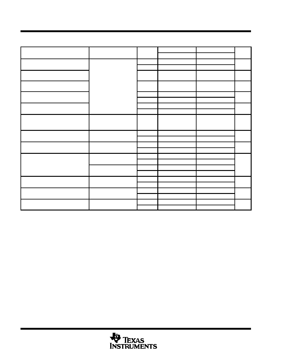
TLC220x, TLC220xA, TLC220xB, TLC220xY
Advanced LinCMOS
TM
LOW-NOISE PRECISION
OPERATIONAL AMPLIFIERS
SLOS175 ≠ FEBRUARY 1997
22
POST OFFICE BOX 655303
∑
DALLAS, TEXAS 75265
TLC2201I electrical characteristics at specified free-air temperature, V
DD
= 5 V (unless otherwise
noted)
PARAMETER
TEST CONDITIONS
TA
TLC2201AI
TLC2201BI
UNIT
PARAMETER
TEST CONDITIONS
TA
MIN
TYP
MAX
MIN
TYP
MAX
UNIT
VIO
Input offset voltage
25
∞
C
80
200
80
200
µ
A
VIO
In ut offset voltage
Full range
350
350
µ
A
VIO
Temperature coefficient of
Full range
0 5
0 5
µ
V/
∞
C
VIO
input offset voltage
Full range
0.5
0.5
µ
V/
∞
C
Input offset voltage long-term
drift (see Note 4)
VIC = 0,
RS = 50
25
∞
C
0.001
0.005
0.001
0.005
µ
V/mo
IIO
Input offset current
25
∞
C
0.5
0.5
pA
IIO
In ut offset current
Full range
150
150
A
IIB
Input bias current
25
∞
C
1
1
pA
IIB
In ut bias current
Full range
150
150
A
Common mode input voltage
0
0
VICR
Common-mode input voltage
range
RS = 50
Full range
to
to
V
range
2.7
2.7
VOH
Maximum high-level output
RL = 10 k
25
∞
C
4.7
4.8
4.7
4.8
V
VOH
g
voltage
RL = 10 k
Full range
4.7
4.7
V
VOL
Maximum low-level output
IO = 0
25
∞
C
0
50
0
50
mV
VOL
voltage
IO = 0
Full range
50
50
mV
VO = 1 V to 4 V,
25
∞
C
150
315
150
315
AVD
Large-signal differential
O
RL = 500 k
Full range
100
100
V/mV
AVD
g
g
voltage amplification
VO = 1 V to 4 V,
25
∞
C
25
55
25
55
V/mV
O
RL = 10 k
Full range
15
15
CMRR
Common-mode rejection ratio
VIC = VICRmin,
25
∞
C
90
110
90
110
dB
CMRR
Common-mode rejection ratio
VO = 0,
RS = 50
Full range
85
85
dB
kSVR
Supply voltage rejection ratio
VDD = 4 6 V to 16 V
25
∞
C
90
110
90
110
dB
kSVR
y
g
j
(
VDD
±
/
VIO)
VDD = 4.6 V to 16 V
Full range
85
85
dB
IDD
Supply current
VO = 2 5 V
No load
25
∞
C
1
1.5
1
1.5
mA
IDD
Su
ly current
VO = 2.5 V,
No load
Full range
1.5
1.5
mA
Full range is ≠ 40
∞
C to 85
∞
C.
NOTE 4: Typical values are based on the input offset voltage shift observed through 168 hours of operating life test at TA = 150
∞
C extrapolated
to TA = 25
∞
C using the Arrhenius equation and assuming an activation energy of 0.96 eV.

TLC220x, TLC220xA, TLC220xB, TLC220xY
Advanced LinCMOS
TM
LOW-NOISE PRECISION
OPERATIONAL AMPLIFIERS
SLOS175 ≠ FEBRUARY 1997
23
POST OFFICE BOX 655303
∑
DALLAS, TEXAS 75265
TLC2201I operating characteristics at specified free-air temperature, V
DD
= 5 V
PARAMETER
TEST CONDITIONS
TA
TLC2201AI
TLC2210BI
UNIT
PARAMETER
TEST CONDITIONS
TA
MIN
TYP
MAX
MIN
TYP
MAX
UNIT
SR
Slew rate at unity gain
VO = 0.5 V to 2.5 V,
25
∞
C
1.8
2.5
1.8
2.5
V/
µ
s
SR
Slew rate at unity gain
RL = 10 k
,
CL = 100 pF
Full range
1.2
1.2
V/
µ
s
V
Equivalent input noise
f = 10 Hz
25
∞
C
18
35
18
30
nV/
Hz
Vn
q
voltage (see Note 5)
f = 1 kHz
25
∞
C
8
15
8
12
nV/
Hz
VN(PP)
Peak-to-peak equivalent input
f = 0.1 to 1 Hz
25
∞
C
0.5
0.5
µ
V
VN(PP)
q
noise voltage
f = 0.1 to 10 Hz
25
∞
C
0.7
0.7
µ
V
In
Equivalent input noise current
25
∞
C
0.6
0.6
fA/
Hz
Gain bandwidth product
f = 10 kHz,
RL = 10 k
,
25
∞
C
1 8
1 8
MHz
Gain-bandwidth product
,
CL = 100 pF
L
25
∞
C
1.8
1.8
MHz
Phase margin at unity gain
RL = 10 k
CL = 100 pF
25
∞
C
45
∞
45
∞
m
Phase margin at unity gain
RL = 10 k
,
CL = 100 pF
25
∞
C
45
∞
45
∞
Full range is ≠ 40
∞
C to 85
∞
C.
NOTE 5: This parameter is tested on a sample basis for the TLC2201A and on all devices for the TLC2201B. For other test requirements, please
contact the factory. This statement has no bearing on testing or nontesting of other parameters.

TLC220x, TLC220xA, TLC220xB, TLC220xY
Advanced LinCMOS
TM
LOW-NOISE PRECISION
OPERATIONAL AMPLIFIERS
SLOS175 ≠ FEBRUARY 1997
24
POST OFFICE BOX 655303
∑
DALLAS, TEXAS 75265
TLC2202I electrical characteristics at specified free-air temperature, V
DD
±
=
±
5 V (unless otherwise
noted)
PARAMETER
TEST CONDITIONS
TA
TLC2202I
UNIT
PARAMETER
TEST CONDITIONS
TA
MIN
TYP
MAX
UNIT
VIO
Input offset voltage
25
∞
C
100
1000
µ
V
VIO
Input offset voltage
VIC = 0
RS = 50
Full range
1200
µ
V
VIO
Temperature coefficient of input offset voltage
VIC = 0,
RS = 50
Full range
0.5
µ
V/
∞
C
Input offset voltage long-term drift (see Note 4)
25
∞
C
0.001
0.005
µ
V/mo
IIO
Input offset current
Full range
150
IIB
Input bias current
VIC = 0,
RS = 50
25
∞
C
1
pA
IIB
Input bias current
Full range
150
≠ 5
VICR
Common-mode input voltage range
RS = 50
Full range
to
V
ICR
g
g
S
g
2.7
VOM
Maximum positive peak output voltage swing
25
∞
C
4.7
4.8
VOM + Maximum positive peak output voltage swing
RL = 10 k
Full range
4.7
V
VOM
Maximum negative peak output voltage swing
RL = 10 k
25
∞
C
≠ 4.7
≠ 4.9
VOM ≠ Maximum negative peak output voltage swing
Full range
≠ 4.7
V
VO =
±
4 V
RL = 500 k
25
∞
C
300
560
AVD
Large signal differential voltage amplification
VO =
±
4 V,
RL = 500 k
Full range
150
V/mV
AVD
Large-signal differential voltage amplification
VO =
±
4 V
RL = 10 k
25
∞
C
50
100
V/mV
VO =
±
4 V,
RL = 10 k
Full range
25
CMRR
Common mode rejection ratio
VO = 0,
VIC = VICRmin,
25
∞
C
80
115
dB
CMRR
Common-mode rejection ratio
O
,
IC
ICR
,
RS = 50
Full range
80
dB
kSVR
Supply voltage rejection ratio (
VDD
±
/
VIO)
VDD =
±
2 3 V to
±
8 V
25
∞
C
80
110
dB
kSVR
Supply-voltage rejection ratio (
VDD
±
/
VIO)
VDD =
±
2.3 V to
±
8 V
Full range
80
dB
IDD
Supply current
VO = 0
No load
25
∞
C
1.8
2.7
mA
IDD
Supply current
VO = 0,
No load
Full range
2.7
mA
Full range is ≠ 40
∞
C to 85
∞
C.
NOTE 4: Typical values are based on the input offset voltage shift observed through 168 hours of operating life test at TA = 150
∞
C extrapolated
to TA = 25
∞
C using the Arrhenius equation and assuming an activation energy of 0.96 eV.
TLC2202I operating characteristics at specified free-air temperature, V
DD
±
=
±
5 V
PARAMETER
TEST CONDITIONS
TA
TLC2202I
UNIT
PARAMETER
TEST CONDITIONS
TA
MIN
TYP
MAX
UNIT
SR
Slew rate at unity gain
VO =
±
2.3 V,
RL = 10 k
,
25
∞
C
1.8
2.7
V/
µ
s
SR
Slew rate at unity gain
O
,
CL = 100 pF
L
,
Full range
1.2
V/
µ
s
V
Equivalent input noise voltage
f = 10 Hz
25
∞
C
18
nV/
Hz
Vn
Equivalent input noise voltage
f = 1 kHz
25
∞
C
8
nV/
Hz
VN(PP)
Peak to peak equivalent input noise voltage
f = 0.1 to 1 Hz
25
∞
C
0.5
µ
V
VN(PP)
Peak-to-peak equivalent input noise voltage
f = 0.1 to 10 Hz
25
∞
C
0.7
µ
V
In
Equivalent input noise current
25
∞
C
0.6
fA/
Hz
Gain bandwidth product
f = 10 kHz,
RL = 10 k
,
25
∞
C
1 9
MHz
Gain-bandwidth product
,
CL = 100 pF
L
,
25
∞
C
1.9
MHz
m
Phase margin at unity gain
RL = 10 k
,
CL = 100 pF
25
∞
C
48
∞
Full range is ≠ 40
∞
C to 85
∞
C.
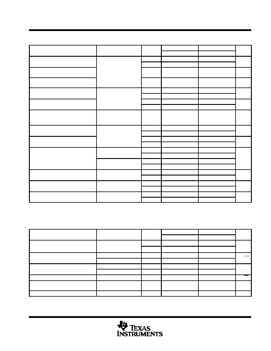
TLC220x, TLC220xA, TLC220xB, TLC220xY
Advanced LinCMOS
TM
LOW-NOISE PRECISION
OPERATIONAL AMPLIFIERS
SLOS175 ≠ FEBRUARY 1997
25
POST OFFICE BOX 655303
∑
DALLAS, TEXAS 75265
TLC2202I electrical characteristics at specified free-air temperature, V
DD
±
=
±
5 V (unless otherwise
noted)
PARAMETER
TEST CONDITIONS
TA
TLC2202AI
TLC2202BI
UNIT
PARAMETER
TEST CONDITIONS
TA
MIN
TYP
MAX
MIN
TYP
MAX
UNIT
VIO
Input offset voltage
25
∞
C
80
500
80
500
µ
V
VIO
In ut offset voltage
Full range
700
700
µ
V
VIO
Temperature coefficient
VIC = 0
RS = 50
Full range
0 5
0 5
µ
V/
∞
C
VIO
of input offset voltage
VIC = 0,
RS = 50
Full range
0.5
0.5
µ
V/
∞
C
Input offset voltage long-term
drift (see Note 4)
25
∞
C
0.001
0.005
0.001
0.005
µ
V/mo
IIO
Input offset current
25
∞
C
0.5
0.5
pA
IIO
In ut offset current
VIC = 0
RS = 50
Full range
150
150
A
IIB
Input bias current
VIC = 0,
RS = 50
25
∞
C
1
1
pA
IIB
In ut bias current
Full range
150
150
A
Common mode input
≠ 5
≠ 5
VICR
Common-mode input
voltage range
RS = 50
Full range
to
to
V
voltage range
2.7
2.7
VOM
Maximum positive peak
25
∞
C
4.7
4.8
4.7
4.8
V
VOM +
output voltage swing
RL = 10 k
Full range
4.7
4.7
V
VOM
Maximum negative peak
RL = 10 k
25
∞
C
≠ 4.7
≠ 4.9
≠ 4.7
≠ 4.9
V
VOM ≠
g
output voltage swing
Full range
≠ 4.7
≠ 4.7
V
VO =
±
4 V,
25
∞
C
300
560
300
560
AVD
Large-signal differential
O
RL = 500 k
Full range
150
150
V/mV
AVD
g
g
voltage amplification
VO =
±
4 V,
25
∞
C
50
100
50
100
V/mV
O
RL = 10 k
Full range
25
25
CMRR
Common-mode rejection ratio
VIC = VICRmin,
25
∞
C
80
115
80
115
dB
CMRR
Common-mode rejection ratio
IC
ICR
VO = 0,
RS = 50
Full range
80
80
dB
kSVR
Supply-voltage rejection ratio
VDD
± ±
2 3 V to
±
8 V
25
∞
C
80
110
80
110
dB
kSVR
y
g
j
(
VDD
±
/
VIO)
VDD
±
±
2.3 V to
±
8 V
Full range
80
80
dB
IDD
Supply current
VO = 0
No load
25
∞
C
1.8
2.7
1.8
2.7
mA
IDD
Su
ly current
VO = 0,
No load
Full range
2.7
2.7
mA
Full range is ≠ 40
∞
C to 85
∞
C.
NOTE 4: Typical values are based on the input offset voltage shift observed through 168 hours of operating life test at TA = 150
∞
C extrapolated
to TA = 25
∞
C using the Arrhenius equation and assuming an activation energy of 0.96 eV.
TLC2202I operating characteristics at specified free-air temperature, V
DD
±
=
±
5 V
PARAMETER
TEST CONDITIONS
TA
TLC2202AI
TLC2202BI
UNIT
PARAMETER
TEST CONDITIONS
TA
MIN
TYP
MAX
MIN
TYP
MAX
UNIT
V
±
2 3 V R
10 k
25
∞
C
1 8
2 7
1 8
2 7
SR
Slew rate at unity gain
VO =
±
2.3 V, RL = 10 k
,
25
∞
C
1.8
2.7
1.8
2.7
V/
µ
s
SR
Slew rate at unity gain
O
L
CL = 100 pF
Full range
1.2
1.2
V/
µ
s
Vn
Equivalent input noise voltage
f = 10 Hz
25
∞
C
18
35
18
30
nV/
Hz
Vn
q
g
(see Note 5)
f = 1 kHz
25
∞
C
8
15
8
12
nV/
Hz
VN(PP)
Peak-to-peak equivalent
f = 0.1 to 1 Hz
25
∞
C
0.5
0.5
µ
V
VN(PP)
q
input noise voltage
f = 0.1 to 10 Hz
25
∞
C
0.7
0.7
µ
V
In
Equivalent input noise current
25
∞
C
0.6
0.6
fA/
Hz
f = 10 kHz
RL = 10 k
Gain-bandwidth product
f = 10 kHz,
RL = 10 k
,
C
100 pF
25
∞
C
1.9
1.9
MHz
CL = 100 pF
m
Phase margin at unity gain
RL = 10 k
CL = 100 pF
25
∞
C
48
∞
48
∞
m
Phase margin at unity gain
RL = 10 k
, CL = 100 F
25
∞
C
48
∞
48
∞
Full range is ≠ 40
∞
C to 85
∞
C.
NOTE 5: This parameter is tested on a sample basis for the TLC2202A and on all devices for the TLC2202B. For other test requirements, please
contact the factory. This statement has no bearing on testing or nontesting of other parameters.

TLC220x, TLC220xA, TLC220xB, TLC220xY
Advanced LinCMOS
TM
LOW-NOISE PRECISION
OPERATIONAL AMPLIFIERS
SLOS175 ≠ FEBRUARY 1997
26
POST OFFICE BOX 655303
∑
DALLAS, TEXAS 75265
TLC2202I electrical characteristics at specified free-air temperature, V
DD
= 5 V (unless otherwise
noted)
PARAMETER
TEST CONDITIONS
TA
TLC2202I
UNIT
PARAMETER
TEST CONDITIONS
TA
MIN
TYP
MAX
UNIT
VIO
Input offset voltage
25
∞
C
100
1000
µ
V
VIO
Input offset voltage
VIC = 0
RS = 50
Full range
1200
µ
V
VIO
Temperature coefficient of input offset voltage
VIC = 0,
RS = 50
Full range
0.5
µ
V/
∞
C
Input offset voltage long-term drift (see Note 4)
25
∞
C
0.001
0.005
µ
V/mo
IIO
Input offset current
Full range
150
IIB
Input bias current
VIC = 0,
RS = 50
25
∞
C
1
pA
IIB
Input bias current
Full range
150
0
VICR
Common-mode input voltage range
RS = 50
Full range
to
V
ICR
g
g
S
g
2.7
VOH
Maximum high level output voltage
RL = 10 k
25
∞
C
4.7
4.8
V
VOH
Maximum high-level output voltage
RL = 10 k
Full range
4.7
V
VOL
Maximum low level output voltage
IO = 0
25
∞
C
0
50
mV
VOL
Maximum low-level output voltage
IO = 0
Full range
50
mV
VO =1 V to 4 V,
25
∞
C
150
315
AVD
Large signal differential voltage amplification
O
,
RL = 500 k
Full range
100
V/mV
AVD
Large-signal differential voltage amplification
VO = 1 V to 4 V,
25
∞
C
25
55
V/mV
O
,
RL = 10 k
Full range
15
CMRR
Common mode rejection ratio
VO = 0,
VIC = VICRmin,
25
∞
C
75
110
dB
CMRR
Common-mode rejection ratio
O
,
IC
ICR
,
RS = 50
Full range
75
dB
kSVR
Supply voltage rejection ratio (
VDD
±
/
VIO)
VDD= 4 6 V to 16 V
25
∞
C
80
110
dB
kSVR
Supply-voltage rejection ratio (
VDD
±
/
VIO)
VDD= 4.6 V to 16 V
Full range
80
dB
IDD
Supply current
VO = 2 5 V
No load
25
∞
C
1.7
2.6
mA
IDD
Supply current
VO = 2.5 V,
No load
Full range
2.6
mA
Full range is ≠ 40
∞
C to 85
∞
C.
NOTE 4: Typical values are based on the input offset voltage shift observed through 168 hours of operating life test at TA = 150
∞
C extrapolated
to TA = 25
∞
C using the Arrhenius equation and assuming an activation energy of 0.96 eV.
TLC2202I operating characteristics at specified free-air temperature, V
DD
= 5 V
PARAMETER
TEST CONDITIONS
TA
TLC2202I
UNIT
PARAMETER
TEST CONDITIONS
TA
MIN
TYP
MAX
UNIT
SR
Slew rate at unity gain
VO = 0.5 V to 2.5 V,
25
∞
C
1.6
2.5
V/
µ
s
SR
Slew rate at unity gain
O
,
RL = 10 k
,
CL = 100 pF
Full range
1
V/
µ
s
V
Equivalent input noise voltage
f = 10 Hz
25
∞
C
18
nV/
Hz
Vn
Equivalent input noise voltage
f = 1 kHz
25
∞
C
8
nV/
Hz
VN(PP)
Peak to peak equivalent input noise voltage
f = 0.1 to 1 Hz
25
∞
C
0.5
µ
V
VN(PP)
Peak-to-peak equivalent input noise voltage
f = 0.1 to 10 Hz
25
∞
C
0.7
µ
V
In
Equivalent input noise current
25
∞
C
0.6
fA/
Hz
Gain bandwidth product
f = 10 kHz,
RL = 10 k
,
25
∞
C
1 9
MHz
Gain-bandwidth product
,
CL = 100 pF
L
,
25
∞
C
1.9
MHz
m
Phase margin at unity gain
RL = 10 k
,
CL = 100 pF
25
∞
C
47
∞
Full range is ≠ 40
∞
C to 85
∞
C.
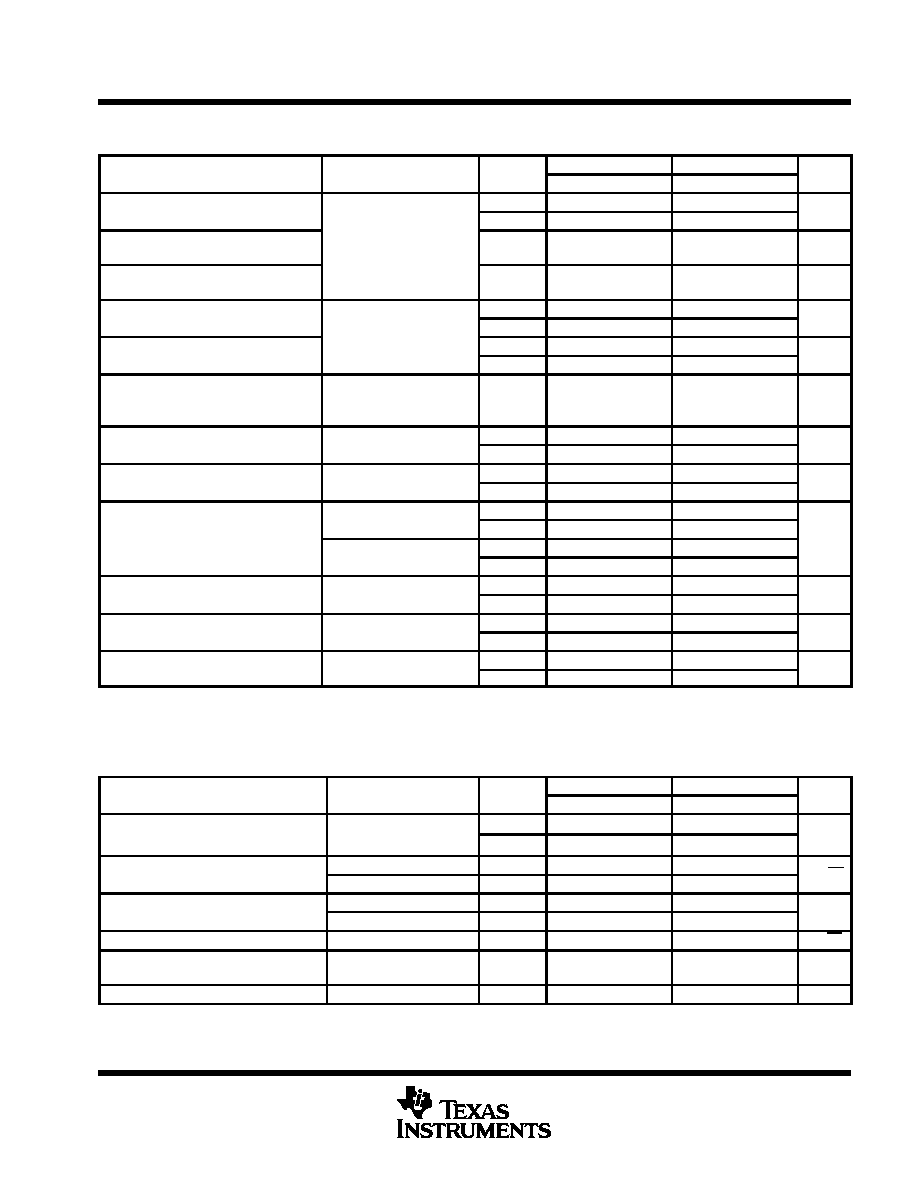
TLC220x, TLC220xA, TLC220xB, TLC220xY
Advanced LinCMOS
TM
LOW-NOISE PRECISION
OPERATIONAL AMPLIFIERS
SLOS175 ≠ FEBRUARY 1997
27
POST OFFICE BOX 655303
∑
DALLAS, TEXAS 75265
TLC2202I electrical characteristics at specified free-air temperature, V
DD
= 5 V (unless otherwise
noted)
PARAMETER
TEST CONDITIONS
TA
TLC2202AI
TLC2202BI
UNIT
PARAMETER
TEST CONDITIONS
TA
MIN
TYP
MAX
MIN
TYP
MAX
UNIT
VIO
Input offset voltage
25
∞
C
80
500
80
500
µ
V
VIO
In ut offset voltage
Full range
700
700
µ
V
VIO
Temperature coefficient of
VIC = 0
RS = 50
Full range
0 5
0 5
µ
V/
∞
C
VIO
input offset voltage
VIC = 0,
RS = 50
Full range
0.5
0.5
µ
V/
∞
C
Input offset voltage long-term
drift (see Note 4)
25
∞
C
0.001
0.005
0.001
0.005
µ
V/mo
IIO
Input offset current
25
∞
C
0.5
0.5
pA
IIO
In ut offset current
VIC = 0
RS = 50
Full range
150
150
A
IIB
Input bias current
VIC = 0,
RS = 50
25
∞
C
1
1
pA
IIB
In ut bias current
Full range
150
150
A
Common mode input
0
0
VICR
Common-mode input
voltage range
RS = 50
Full range
to
to
V
voltage range
2.7
2.7
VOH
Maximum high-level output
RL = 10 k
25
∞
C
4.7
4.8
4.7
4.8
V
VOH
g
voltage
RL = 10 k
Full range
4.7
4.7
V
VOL
Maximum low-level output
IO = 0
25
∞
C
0
50
0
50
mV
VOL
voltage
IO = 0
Full range
50
50
mV
VO = 1 V to 4 V,
25
∞
C
150
315
150
315
AVD
Large-signal differential
O
RL = 500 k
Full range
100
100
V/mV
AVD
g
g
voltage amplification
VO =1 V to 4 V,
25
∞
C
25
55
25
55
V/mV
O
RL = 10 k
Full range
15
15
CMRR
Common-mode rejection ratio
VIC = VICRmin,
25
∞
C
75
110
75
110
dB
CMRR
Common-mode rejection ratio
IC
ICR
VO = 0,
RS = 50
Full range
75
75
dB
kSVR
Supply-voltage rejection ratio
VDD = 4 6 V to 16 V
25
∞
C
80
110
80
110
dB
kSVR
y
g
j
(
VDD
±
/
VIO)
VDD = 4.6 V to 16 V
Full range
80
80
dB
IDD
Supply current
VO = 2 5 V
No load
25
∞
C
1.7
2.6
1.7
2.6
mA
IDD
Su
ly current
VO = 2.5 V,
No load
Full range
2.6
2.6
mA
Full range is ≠ 40
∞
C to 85
∞
C
NOTE 4: Typical values are based on the input offset voltage shift observed through 168 hours of operating life test at TA = 150
∞
C extrapolated
to TA = 25
∞
C using the Arrhenius equation and assuming an activation energy of 0.96 eV.
TLC2202I operating characteristics at specified free-air temperature, V
DD
= 5 V
PARAMETER
TEST CONDITIONS
TA
TLC2202AI
TLC2202BI
UNIT
PARAMETER
TEST CONDITIONS
TA
MIN
TYP
MAX
MIN
TYP
MAX
UNIT
V
0 5 V to 2 5 V
25
∞
C
1 6
2 5
1 6
2 5
SR
Slew rate at unity gain
VO = 0.5 V to 2.5 V,
25
∞
C
1.6
2.5
1.6
2.5
V/
µ
s
SR
Slew rate at unity gain
O
RL = 10 k
, CL = 100 pF
Full range
1
1
V/
µ
s
Vn
Equivalent input noise voltage
f = 10 Hz
25
∞
C
18
35
18
30
nV/
Hz
Vn
q
g
(see Note 5)
f = 1 kHz
25
∞
C
8
15
8
12
nV/
Hz
VN(PP)
Peak-to-peak equivalent
f = 0.1 to 1 Hz
25
∞
C
0.5
0.5
µ
V
VN(PP)
q
input noise voltage
f = 0.1 to 10 Hz
25
∞
C
0.7
0.7
µ
V
In
Equivalent input noise current
25
∞
C
0.6
0.6
fA/
Hz
f = 10 kHz
RL = 10 k
Gain-bandwidth product
f = 10 kHz,
RL = 10 k
,
C
100 pF
25
∞
C
1.9
1.9
MHz
CL = 100 pF
m
Phase margin at unity gain
RL = 10 k
CL = 100 pF
25
∞
C
47
∞
47
∞
m
Phase margin at unity gain
RL = 10 k
, CL = 100 F
25
∞
C
47
∞
47
∞
Full range is ≠ 40
∞
C to 85
∞
C
NOTE 5: This parameter is tested on a sample basis for the TLC2202A and on all devices for the TLC2202B. For other test requirements, please
contact the factory. This statement has no bearing on testing or nontesting of other parameters.
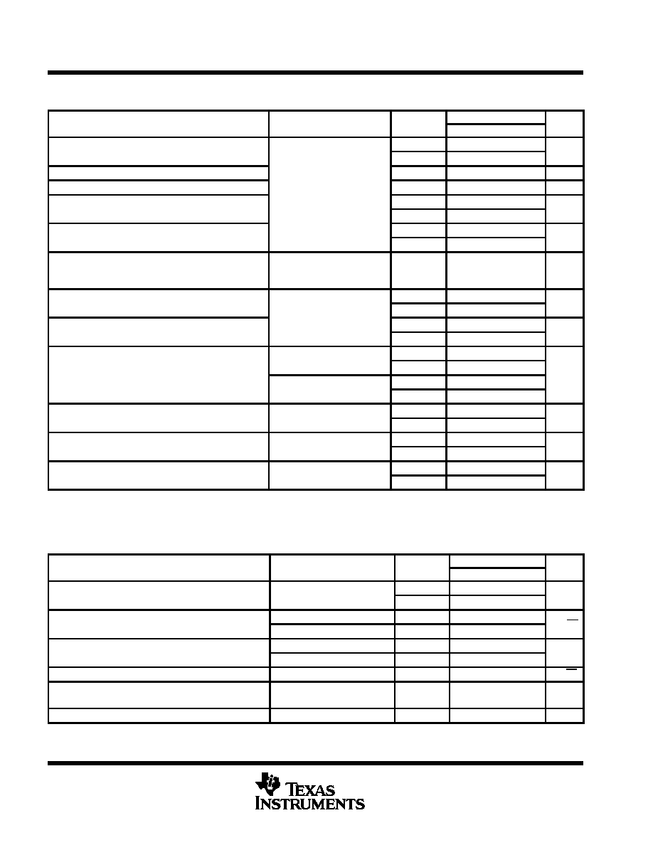
TLC220x, TLC220xA, TLC220xB, TLC220xY
Advanced LinCMOS
TM
LOW-NOISE PRECISION
OPERATIONAL AMPLIFIERS
SLOS175 ≠ FEBRUARY 1997
28
POST OFFICE BOX 655303
∑
DALLAS, TEXAS 75265
TLC2201M electrical characteristics at specified free-air temperature, V
DD
±
=
±
5 V (unless
otherwise noted)
PARAMETER
TEST CONDITIONS
TA
TLC2201M
UNIT
PARAMETER
TEST CONDITIONS
TA
MIN
TYP
MAX
UNIT
VIO
Input offset voltage
25
∞
C
100
500
µ
V
VIO
Input offset voltage
Full range
700
µ
V
VIO
Temperature coefficient of input offset voltage
Full range
0.5
µ
V/
∞
C
Input offset voltage long-term drift (see Note 4)
VIC = 0
RS = 50
25
∞
C
0.001
0.005
µ
V/mo
IIO
Input offset current
VIC = 0,
RS = 50
25
∞
C
0.5
pA
IIO
Input offset current
Full range
500
pA
IIB
Input bias current
25
∞
C
1
pA
IIB
Input bias current
Full range
500
pA
≠ 5
VICR
Common-mode input voltage range
RS = 50
Full range
5
to
V
ICR
g
g
S
g
2.7
VOM
Maximum positive peak output voltage swing
25
∞
C
4.7
4.8
V
VOM + Maximum positive peak output voltage swing
RL = 10 k
Full range
4.7
V
VOM
Maximum negative peak output voltage swing
RL = 10 k
25
∞
C
≠ 4.7
≠ 4.9
V
VOM ≠ Maximum negative peak output voltage swing
Full range
≠ 4.7
V
VO =
±
4 V
RL = 500 k
25
∞
C
400
560
AVD
Large signal differential voltage amplification
VO =
±
4 V,
RL = 500 k
Full range
200
V/mV
AVD
Large-signal differential voltage amplification
VO =
±
4 V
RL = 10 k
25
∞
C
90
100
V/mV
VO =
±
4 V,
RL = 10 k
Full range
45
CMRR
Common mode rejection ratio
VIC = VICRmin,
25
∞
C
90
115
dB
CMRR
Common-mode rejection ratio
VO = 0,
RS = 50
Full range
85
dB
kSVR
Supply voltage rejection ratio (
VDD
±
/
VIO)
VDD
±
=
±
2 3 V to
±
8 V
25
∞
C
90
110
dB
kSVR
Supply voltage rejection ratio (
VDD
±
/
VIO)
VDD
±
=
±
2.3 V to
±
8 V
Full range
85
dB
IDD
Supply current
VO = 0
No load
25
∞
C
1.1
1.5
mA
IDD
Supply current
VO = 0,
No load
Full range
1.5
mA
Full range is ≠ 55
∞
C to 125
∞
C.
NOTE 4: Typical values are based on the input offset voltage shift observed through 168 hours of operating life test at TA = 150
∞
C extrapolated
to TA = 25
∞
C using the Arrhenius equation and assuming an activation energy of 0.96 eV.
TLC2201M operating characteristics at specified free-air temperature, V
DD
±
=
±
5 V
PARAMETER
TEST CONDITIONS
TA
TLC2201M
UNIT
PARAMETER
TEST CONDITIONS
TA
MIN
TYP
MAX
UNIT
SR
Slew rate at unity gain
VO =
±
2.3 V,
RL = 10 k
,
25
∞
C
2
2.7
V/
µ
s
SR
Slew rate at unity gain
CL = 100 pF
Full range
1.3
V/
µ
s
V
Equivalent input noise voltage
f = 10 Hz
25
∞
C
18
nV/
Hz
Vn
Equivalent input noise voltage
f = 1 kHz
25
∞
C
8
nV/
Hz
VN(PP)
Peak to peak equivalent input noise voltage
f = 0.1 to 1 Hz
25
∞
C
0.5
µ
V
VN(PP)
Peak-to-peak equivalent input noise voltage
f = 0.1 to 10 Hz
25
∞
C
0.7
µ
V
In
Equivalent input noise current
25
∞
C
0.6
fA/
Hz
Gain bandwidth product
f = 10 kHz,
RL = 10 k
,
25
∞
C
1 9
MHz
Gain-bandwidth product
CL = 100 pF
L
25
∞
C
1.9
MHz
m
Phase margin
RL = 10 k
,
CL = 100 pF
25
∞
C
48
∞
Full range is ≠ 55
∞
C to 125
∞
C.

TLC220x, TLC220xA, TLC220xB, TLC220xY
Advanced LinCMOS
TM
LOW-NOISE PRECISION
OPERATIONAL AMPLIFIERS
SLOS175 ≠ FEBRUARY 1997
29
POST OFFICE BOX 655303
∑
DALLAS, TEXAS 75265
TLC2201M electrical characteristics at specified free-air temperature, V
DD
±
=
±
5 V (unless
otherwise noted)
PARAMETER
TEST CONDITIONS
TA
TLC2201AM
TLC2210BM
UNIT
PARAMETER
TEST CONDITIONS
TA
MIN
TYP
MAX
MIN
TYP
MAX
UNIT
VIO
Input offset voltage
25
∞
C
80
200
80
200
µ
V
VIO
Input offset voltage
Full range
400
400
µ
V
VIO
Temperature coefficient of
Full range
0 5
0 5
µ
V/
∞
C
VIO
input offset voltage
Full range
0.5
0.5
µ
V/
∞
C
Input offset voltage
long-term drift (see Note 4)
VIC = 0,
RS = 50
25
∞
C
0.001
0.005
0.001
0.005
µ
V/mo
IIO
Input offset current
25
∞
C
0.5
0.5
pA
IIO
Input offset current
Full range
500
500
pA
IIB
Input bias current
25
∞
C
1
1
pA
IIB
Input bias current
Full range
500
500
pA
Common mode input
≠ 5
≠ 5
VICR
Common-mode input
voltage range
RS = 50
Full range
5
to
5
to
V
ICR
voltage range
S
g
2.7
2.7
VOM
Maximum positive peak
25
∞
C
4.7
4.8
4.7
4.8
V
VOM+
output voltage swing
RL = 10 k
Full range
4.7
4.7
V
VOM
Maximum negative peak
RL = 10 k
25
∞
C
≠ 4.7
≠ 4.9
≠ 4.7
≠ 4.9
V
VOM ≠
g
output voltage swing
Full range
≠ 4.7
≠ 4.7
V
VO =
±
4 V,
25
∞
C
400
560
400
560
AVD
Large-signal differential
O
,
RL = 500 k
Full range
200
200
V/mV
AVD
g
g
voltage amplification
VO =
±
4 V,
25
∞
C
90
100
90
100
V/mV
O
,
RL = 10 k
Full range
45
45
CMRR
Common-mode rejection
VIC = VICRmin,
25
∞
C
90
115
90
115
dB
CMRR
j
ratio
VO = 0,
RS = 50
Full range
85
85
dB
kSVR
Supply voltage rejection
VDD
±
=
±
2 3 V to
±
8 V
25
∞
C
90
110
90
110
dB
kSVR
y
g
j
ratio (
VDD
±
/
VIO)
VDD
±
=
±
2.3 V to
±
8 V
Full range
85
85
dB
IDD
Supply current
VO = 0
No load
25
∞
C
1.1
1.5
1.1
1.5
mA
IDD
Supply current
VO = 0,
No load
Full range
1.5
1.5
mA
Full range is ≠ 55
∞
C to 125
∞
C.
NOTE 4: Typical values are based on the input offset voltage shift observable through 168 hours of operating life test at TA = 150
∞
C extrapolated
to TA = 25
∞
C using the Arrhenius equation and assuming an activation energy of 0.96 eV.
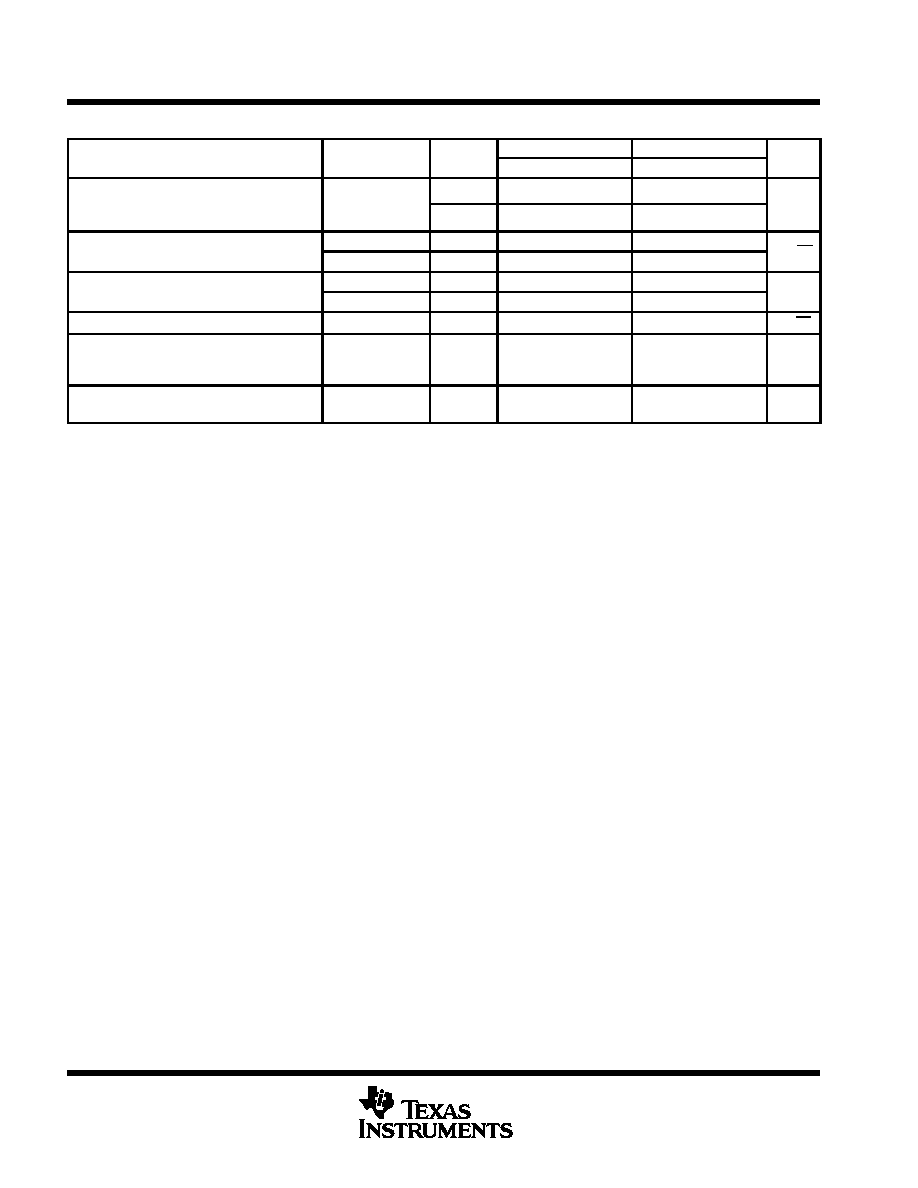
TLC220x, TLC220xA, TLC220xB, TLC220xY
Advanced LinCMOS
TM
LOW-NOISE PRECISION
OPERATIONAL AMPLIFIERS
SLOS175 ≠ FEBRUARY 1997
30
POST OFFICE BOX 655303
∑
DALLAS, TEXAS 75265
TLC2201M operating characteristics at specified free-air temperature, V
DD
±
=
±
5 V
PARAMETER
TEST
TA
TLC2201AM
TLC2201BM
UNIT
PARAMETER
CONDITIONS
TA
MIN
TYP
MAX
MIN
TYP
MAX
UNIT
VO =
±
2 3 V
25
∞
C
2
2 7
2
2 7
SR
Slew rate at unity gain
VO =
±
2.3 V,
RL 10 k
25
∞
C
2
2.7
2
2.7
V/
µ
s
SR
Slew rate at unity gain
RL = 10 k
,
CL = 100 pF
Full range
1.3
1.3
V/
µ
s
V
Equivalent input noise voltage
f = 10 Hz
25
∞
C
18
35
18
30
nV/
Hz
Vn
q
g
(see Note 5)
f = 1 kHz
25
∞
C
8
15
8
12
nV/
Hz
VN(PP)
Peak-to-peak equivalent input
f = 0.1 to 1 Hz
25
∞
C
0.5
0.5
µ
V
VN(PP)
q
noise voltage
f = 0.1 to 10 Hz
25
∞
C
0.7
0.7
µ
V
In
Equivalent input noise current
25
∞
C
0.6
0.6
fA/
Hz
f = 10 kHz,
Gain-bandwidth product
f 10 kHz,
RL = 10 k
,
25
∞
C
1.9
1.9
MHz
L
,
CL = 100 pF
Phase margin at unity gain
RL = 10 k
,
25
∞
C
48
∞
48
∞
m
Phase margin at unity gain
L
CL = 100 pF
25
∞
C
48
∞
48
∞
Full range is ≠ 55
∞
C to 125
∞
C.
NOTE 5: This parameter is tested on a sample basis for the TLC2201A and on all devices for the TLC2201B. For other test requirements, please
contact the factory. This statement has no bearing on testing or nontesting of other parameters.

TLC220x, TLC220xA, TLC220xB, TLC220xY
Advanced LinCMOS
TM
LOW-NOISE PRECISION
OPERATIONAL AMPLIFIERS
SLOS175 ≠ FEBRUARY 1997
31
POST OFFICE BOX 655303
∑
DALLAS, TEXAS 75265
TLC2201M electrical characteristics at specified free-air temperature, V
DD
= 5 V (unless otherwise
noted)
PARAMETER
TEST CONDITIONS
TA
TLC2201M
UNIT
PARAMETER
TEST CONDITIONS
TA
MIN
TYP
MAX
UNIT
VIO
Input offset voltage
25
∞
C
100
500
µ
V
VIO
Input offset voltage
Full range
700
µ
V
VIO
Temperature coefficient of input offset voltage
Full range
0.5
µ
V/
∞
C
Input offset voltage long-term drift (see Note 4)
VIC = 0
RS = 50
25
∞
C
0.001
0.005*
µ
V/mo
IIO
Input offset current
VIC = 0,
RS = 50
25
∞
C
0.5
pA
IIO
Input offset current
Full range
500
pA
IIB
Input bias current
25
∞
C
1
pA
IIB
Input bias current
Full range
500
pA
0
VICR
Common-mode input voltage range
RS = 50
Full range
0
to
V
ICR
g
g
S
g
2.7
VOH
Maximum high level output voltage
RL = 10 k
25
∞
C
4.7
4.8
V
VOH
Maximum high-level output voltage
RL = 10 k
Full range
4.7
V
VOL
Maximum low level output voltage
IO = 0
25
∞
C
0
50
mV
VOL
Maximum low-level output voltage
IO = 0
Full range
50
mV
VO = 1 V to 4 V,
25
∞
C
150
315
AVD
Large signal differential voltage amplification
O
,
RL = 500 k
Full range
75
V/mV
AVD
Large-signal differential voltage amplification
VO = 1 V to 4 V,
25
∞
C
25
55
V/mV
O
,
RL = 10 k
Full range
10
CMRR
Common mode rejection ratio
VIC = VICRmin,
25
∞
C
90
110
dB
CMRR
Common-mode rejection ratio
VO = 0,
RS = 50
Full range
85
dB
kSVR
Supply voltage rejection ratio (
VDD
±
/
VIO)
VDD = 4 6 V to 16 V
25
∞
C
90
110
dB
kSVR
Supply voltage rejection ratio (
VDD
±
/
VIO)
VDD = 4.6 V to 16 V
Full range
85
dB
IDD
Supply current
VO = 2 5 V
No load
25
∞
C
1
1.5
mA
IDD
Supply current
VO = 2.5 V,
No load
Full range
1.5
mA
On products compliant to MIL-PRF-38535, Class B, this parameter is not production tested.
Full range is ≠ 55
∞
C to 125
∞
C.
NOTE 4: Typical values are based on the input offset voltage shift observed through 168 hours of operating life test at TA = 150
∞
C extrapolated
to TA = 25
∞
C using the Arrhenius equation and assuming an activation energy of 0.96 eV.
TLC2201M operating characteristics at specified free-air temperature, V
DD
= 5 V
PARAMETER
TEST CONDITIONS
TA
TLC2201M
UNIT
PARAMETER
TEST CONDITIONS
TA
MIN
TYP
MAX
UNIT
SR
Slew rate at unity gain
VO = 0.5 V to 2.5 V,
25
∞
C
1.8
2.5
V/
µ
s
SR
Slew rate at unity gain
RL = 10 k
,
CL = 100 pF
Full range
1.1
V/
µ
s
V
Equivalent input noise voltage
f = 10 Hz
25
∞
C
18
nV/
Hz
Vn
Equivalent input noise voltage
f = 1 kHz
25
∞
C
8
nV/
Hz
VN(PP)
Peak to peak equivalent input noise voltage
f = 0.1 to 1 Hz
25
∞
C
0.5
µ
V
VN(PP)
Peak-to-peak equivalent input noise voltage
f = 0.1 to 10 Hz
25
∞
C
0.7
µ
V
In
Equivalent input noise current
25
∞
C
0.6
fA/
Hz
Gain bandwidth product
f = 10 kHz,
RL = 10 k
,
25
∞
C
1 8
MHz
Gain-bandwidth product
CL = 100 pF
L
25
∞
C
1.8
MHz
m
Phase margin at unity gain
RL = 10 k
,
CL = 100 pF
25
∞
C
45
∞
Full range is ≠ 55
∞
C to 125
∞
C.

TLC220x, TLC220xA, TLC220xB, TLC220xY
Advanced LinCMOS
TM
LOW-NOISE PRECISION
OPERATIONAL AMPLIFIERS
SLOS175 ≠ FEBRUARY 1997
32
POST OFFICE BOX 655303
∑
DALLAS, TEXAS 75265
TLC2201M electrical characteristics at specified free-air temperature, V
DD
= 5 V (unless otherwise
noted)
PARAMETER
TEST CONDITIONS
TA
TLC2201AM
TLC2210BM
UNIT
PARAMETER
TEST CONDITIONS
TA
MIN
TYP
MAX
MIN
TYP
MAX
UNIT
VIO
Input offset voltage
25
∞
C
80
200
80
200
µ
V
VIO
Input offset voltage
Full range
400
400
µ
V
VIO
Temperature coefficient of
Full range
0 5
0 5
µ
V/
∞
C
VIO
input offset voltage
Full range
0.5
0.5
µ
V/
∞
C
Input offset voltage
long-term drift (see Note 4)
VIC = 0,
RS = 50
25
∞
C
0.001
0.005
0.001
0.005
µ
V/mo
IIO
Input offset current
25
∞
C
0.5
0.5
pA
IIO
Input offset current
Full range
500
500
pA
IIB
Input bias current
25
∞
C
1
1
pA
IIB
Input bias current
Full range
500
500
pA
Common mode input
0
0
VICR
Common-mode input
voltage range
RS = 50
Full range
0
to
0
to
V
ICR
voltage range
S
g
2.7
2.7
VOH
Maximum high-level output
RL = 10 k
25
∞
C
4.7
4.8
4.7
4.8
V
VOH
g
voltage
RL = 10 k
Full range
4.7
4.7
V
VOL
Maximum low-level output
IO = 0
25
∞
C
0
50
0
50
V
VOL
voltage
IO = 0
Full range
50
50
V
VO = 1 V to 4 V,
25
∞
C
150
315
150
315
AVD
Large-signal differential
O
,
RL = 500 k
Full range
75
75
V/mV
AVD
g
g
voltage amplification
VO = 1 V to 4 V,
25
∞
C
25
55
25
55
V/mV
O
,
RL = 10 k
Full range
10
10
CMRR
Common-mode rejection
VIC = VICRmin,
25
∞
C
90
110
90
110
dB
CMRR
j
ratio
VO = 0,
RS = 50
Full range
85
85
dB
kSVR
Supply voltage rejection
VDD = 4 6 V to 16 V
25
∞
C
90
110
90
110
dB
kSVR
y
g
j
ratio (
VDD
±
/
VIO)
VDD = 4.6 V to 16 V
Full range
85
85
dB
IDD
Supply current
VO = 2 5 V
No load
25
∞
C
1.1
1.5
1.1
1.5
mA
IDD
Supply current
VO = 2.5 V,
No load
Full range
1.5
1.5
mA
Full range is ≠ 55
∞
C to 125
∞
C.
NOTE 4: Typical values are based on the input offset voltage shift observable through 168 hours of operating life test at TA = 150
∞
C extrapolated
to TA = 25
∞
C using the Arrhenius equation and assuming an activation energy of 0.96 eV.
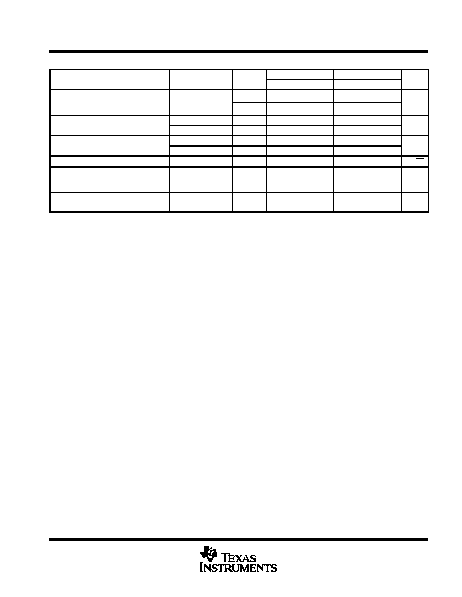
TLC220x, TLC220xA, TLC220xB, TLC220xY
Advanced LinCMOS
TM
LOW-NOISE PRECISION
OPERATIONAL AMPLIFIERS
SLOS175 ≠ FEBRUARY 1997
33
POST OFFICE BOX 655303
∑
DALLAS, TEXAS 75265
TLC2201M operating characteristics at specified free-air temperature, V
DD
= 5 V
PARAMETER
TEST CONDITIONS
TA
TLC2201AM
TLC2201BM
UNIT
PARAMETER
TEST CONDITIONS
TA
MIN
TYP
MAX
MIN
TYP
MAX
UNIT
SR
Slew rate at unity gain
VO = 0.5 V to 2.5 V,
RL 10 k
25
∞
C
1.8
2.5
1.8
2.5
V/
µ
s
SR
Slew rate at unity gain
RL = 10 k
,
CL = 100 pF
Full range
1.1
1.1
V/
µ
s
V
Equivalent input noise voltage
f = 10 Hz
25
∞
C
18
35
18
30
nV/
Hz
Vn
q
g
(see Note 5)
f = 1 kHz
25
∞
C
8
15
8
12
nV/
Hz
VN(PP)
Peak-to-peak equivalent input
f = 0.1 to 1 Hz
25
∞
C
0.5
0.5
µ
V
VN(PP)
q
noise voltage
f = 0.1 to 10 Hz
25
∞
C
0.7
0.7
µ
V
In
Equivalent input noise current
25
∞
C
0.6
0.6
fA/
Hz
f = 10 kHz,
Gain-bandwidth product
f 10 kHz,
RL = 10 k
,
25
∞
C
1.8
1.8
MHz
L
,
CL = 100 pF
Phase margin at unity gain
RL = 10 k
,
25
∞
C
45
∞
45
∞
m
Phase margin at unity gain
L
CL = 100 pF
25
∞
C
45
∞
45
∞
Full range is ≠ 55
∞
C to 125
∞
C.
NOTE 5: This parameter is tested on a sample basis for the TLC2201A and on all devices for the TLC2201B. For other test requirements, please
contact the factory. This statement has no bearing on testing or nontesting of other parameters.
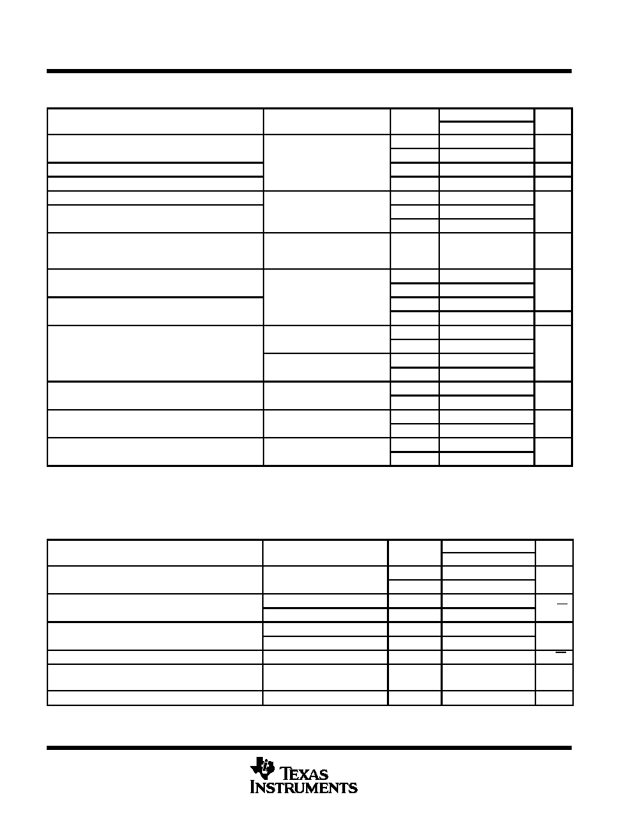
TLC220x, TLC220xA, TLC220xB, TLC220xY
Advanced LinCMOS
TM
LOW-NOISE PRECISION
OPERATIONAL AMPLIFIERS
SLOS175 ≠ FEBRUARY 1997
34
POST OFFICE BOX 655303
∑
DALLAS, TEXAS 75265
TLC2202M electrical characteristics at specified free-air temperature, V
DD
±
=
±
5 V (unless
otherwise noted)
PARAMETER
TEST CONDITIONS
TA
TLC2202M
UNIT
PARAMETER
TEST CONDITIONS
TA
MIN
TYP
MAX
UNIT
VIO
Input offset voltage
25
∞
C
100
1000
µ
V
VIO
Input offset voltage
VIC = 0
RS = 50
Full range
1250
µ
V
VIO
Temperature coefficient of input offset voltage
VIC = 0,
RS = 50
Full range
0.5
µ
V/
∞
C
Input offset voltage long-term drift (see Note 4)
25
∞
C
0.001
0.005*
µ
V/mo
IIO
Input offset current
Full range
500
IIB
Input bias current
VIC = 0,
RS = 50
25
∞
C
1
pA
IIB
Input bias current
Full range
500
≠ 5
VICR
Common-mode input voltage range
RS = 50
Full range
to
V
ICR
g
g
S
g
2.7
VOM
Maximum positive peak output voltage swing
25
∞
C
4.7
4.8
VOM + Maximum positive peak output voltage swing
RL = 10 k
Full range
4.7
V
VOM
Maximum negative peak output voltage swing
RL = 10 k
25
∞
C
≠ 4.7
≠ 4.9
VOM ≠ Maximum negative peak output voltage swing
Full range
≠ 4.7
V
VO =1 V to 4 V,
25
∞
C
300
560
AVD
Large signal differential voltage amplification
O
,
RL = 500 k
Full range
100
V/mV
AVD
Large-signal differential voltage amplification
VO = 1 V to 4 V,
25
∞
C
50
100
V/mV
O
,
RL = 10 k
Full range
25
CMRR
Common mode rejection ratio
VO = 0,
VIC = VICRmin,
25
∞
C
80
115
dB
CMRR
Common-mode rejection ratio
O
,
IC
ICR
,
RS = 50
Full range
80
dB
kSVR
Supply voltage rejection ratio (
VDD
±
/
VIO)
VDD=
±
2 3 V to
±
8 V
25
∞
C
80
110
dB
kSVR
Supply-voltage rejection ratio (
VDD
±
/
VIO)
VDD=
±
2.3 V to
±
8 V
Full range
80
dB
IDD
Supply current
VO = 0
No load
25
∞
C
1.8
2.7
mA
IDD
Supply current
VO = 0,
No load
Full range
2.7
mA
* On products compliant to MIL-PRF-38535, Class B, this parameter is not production tested.
Full range is ≠ 55
∞
C to 125
∞
C.
NOTE 4: Typical values are based on the input offset voltage shift observed through 168 hours of operating life test at TA = 150
∞
C extrapolated
to TA = 25
∞
C using Arrhenius equation and assuming an activation energy of 0.96 eV.
TLC2202M operating characteristics at specified free-air temperature, V
DD
±
=
±
5 V
PARAMETER
TEST CONDITIONS
TA
TLC2202M
UNIT
PARAMETER
TEST CONDITIONS
TA
MIN
TYP
MAX
UNIT
SR
Slew rate at unity gain
VO =
±
2.3 V,
RL = 10 k
,
25
∞
C
1.8
2.7
V/
µ
s
SR
Slew rate at unity gain
O
,
CL = 100 pF
L
,
Full range
1.1
V/
µ
s
V
Equivalent input noise voltage
f = 10 Hz
25
∞
C
18
nV/
Hz
Vn
Equivalent input noise voltage
f = 1 kHz
25
∞
C
8
nV/
Hz
VN(PP)
Peak to peak equivalent input noise voltage
f = 0.1 to 1 Hz
25
∞
C
0.5
µ
V
VN(PP)
Peak-to-peak equivalent input noise voltage
f = 0.1 to 10 Hz
25
∞
C
0.7
µ
V
In
Equivalent input noise current
25
∞
C
0.6
fA/
Hz
Gain bandwidth product
f = 10 kHz,
RL = 10 k
,
25
∞
C
1 9
MHz
Gain-bandwidth product
,
CL = 100 pF
L
,
25
∞
C
1.9
MHz
m
Phase margin at unity gain
RL = 10 k
,
CL = 100 pF
25
∞
C
48
∞
Full range is ≠ 55
∞
C to 125
∞
C.

TLC220x, TLC220xA, TLC220xB, TLC220xY
Advanced LinCMOS
TM
LOW-NOISE PRECISION
OPERATIONAL AMPLIFIERS
SLOS175 ≠ FEBRUARY 1997
35
POST OFFICE BOX 655303
∑
DALLAS, TEXAS 75265
TLC2202M electrical characteristics at specified free-air temperature, V
DD
±
=
±
5 V (unless
otherwise noted)
PARAMETER
TEST CONDITIONS
TA
TLC2202AM
TLC2202BM
UNIT
PARAMETER
TEST CONDITIONS
TA
MIN
TYP
MAX
MIN
TYP
MAX
UNIT
VIO
Input offset voltage
25
∞
C
80
500
80
500
µ
V
VIO
In ut offset voltage
Full range
750
750
µ
V
VIO
Temperature coefficient
VIC = 0
RS = 50
Full range
0 5
0 5
µ
V/
∞
C
VIO
of input offset voltage
VIC = 0,
RS = 50
Full range
0.5
0.5
µ
V/
∞
C
Input offset voltage
long-term drift (see Note 4)
25
∞
C
0.001
0.005*
0.001
0.005*
µ
V/mo
IIO
Input offset current
25
∞
C
0.5
0.5
pA
IIO
In ut offset current
VIC = 0
RS = 50
Full range
500
500
A
IIB
Input bias current
VIC = 0,
RS = 50
25
∞
C
1
1
pA
IIB
In ut bias current
Full range
500
500
A
Common mode input
≠ 5
≠ 5
VICR
Common-mode input
voltage range
RS = 50
Full range
to
to
V
voltage range
2.7
2.7
VOM
Maximum positive peak
25
∞
C
4.7
4.8
4.7
4.8
V
VOM +
output voltage swing
RL = 10 k
Full range
4.7
4.7
V
VOM
Maximum negative peak
RL = 10 k
25
∞
C
≠ 4.7
≠ 4.9
≠ 4.7
≠ 4.9
V
VOM ≠
g
output voltage swing
Full range
≠ 4.7
≠ 4.7
V
VO =
±
4 V,
25
∞
C
300
560
300
560
AVD
Large-signal differential
O
RL = 500 k
Full range
100
100
V/mV
AVD
g
g
voltage amplification
VO =
±
4 V,
25
∞
C
50
100
50
100
V/mV
O
RL = 10 k
Full range
25
25
CMRR
Common-mode rejection
VO = 0, VIC = VICRmin,
25
∞
C
80
115
80
115
dB
CMRR
j
ratio
O
IC
ICR
RS = 50
Full range
80
80
dB
kSVR
Supply-voltage rejection
VDD
±
=
±
2 3 V to
±
8 V
25
∞
C
80
110
80
110
dB
kSVR
y
g
j
ratio (
VDD
±
/
VIO)
VDD
±
=
±
2.3 V to
±
8 V
Full range
80
80
dB
IDD
Supply current
VO = 0
No load
25
∞
C
1.8
2.7
1.8
2.7
mA
IDD
Su
ly current
VO = 0,
No load
Full range
2.7
2.7
mA
* On products compliant to MIL-PRF-38535, Class B, this parameter is not production tested.
Full range is ≠ 55
∞
C to 125
∞
C.
NOTE 4: Typical values are based on the input offset voltage shift observed through 168 hours of operating life test at TA = 150
∞
C extrapolated
to TA = 25
∞
C using the Arrhenius equation and assuming an activation energy of 0.96 eV.

TLC220x, TLC220xA, TLC220xB, TLC220xY
Advanced LinCMOS
TM
LOW-NOISE PRECISION
OPERATIONAL AMPLIFIERS
SLOS175 ≠ FEBRUARY 1997
36
POST OFFICE BOX 655303
∑
DALLAS, TEXAS 75265
TLC2202M operating characteristics at specified free-air temperature, V
DD
±
=
±
5 V
PARAMETER
TEST CONDITIONS
T
TLC2202AM
TLC2202BM
UNIT
PARAMETER
TEST CONDITIONS
TA
MIN
TYP
MAX
MIN
TYP
MAX
UNIT
VO =
±
2 3 V
25
∞
C
1 8
2 7
1 8
2 7
SR
Slew rate at unity gain
VO =
±
2.3 V,
RL 10 k
25
∞
C
1.8
2.7
1.8
2.7
V/
µ
s
SR
Slew rate at unity gain
RL = 10 k
,
CL = 100 pF
Full range
1.1
1.1
V/
µ
s
V
Equivalent input noise voltage
f = 10 Hz
25
∞
C
18
35*
18
30*
nV/
Hz
Vn
q
g
(see Note 5)
f = 1 kHz
25
∞
C
8
15*
8
12*
nV/
Hz
VN(PP)
Peak-to-peak equivalent input
f = 0.1 to 1 Hz
25
∞
C
0.5
0.5
µ
V
VN(PP)
q
noise voltage
f = 0.1 to 10 Hz
25
∞
C
0.7
0.7
µ
V
In
Equivalent input noise current
25
∞
C
0.6
0.6
fA/
Hz
f = 10 kHz,
Gain-bandwidth product
f 10 kHz,
RL = 10 k
,
25
∞
C
1.9
1.9
MHz
L
,
CL = 100 pF
Phase margin at unity gain
RL = 10 k
,
25
∞
C
48
∞
48
∞
m
Phase margin at unity gain
L
CL = 100 pF
25
∞
C
48
∞
48
∞
* On products compliant to MIL-PRF-38535, Class B, this parameter is not production tested.
Full range is ≠ 55
∞
C to 125
∞
C.
NOTE 5: This parameter is tested on a sample basis for the TLC2202A and on all devices for the TLC2202B. For other test requirements, please
contact the factory. This statement has no bearing on testing or nontesting of other parameters.

TLC220x, TLC220xA, TLC220xB, TLC220xY
Advanced LinCMOS
TM
LOW-NOISE PRECISION
OPERATIONAL AMPLIFIERS
SLOS175 ≠ FEBRUARY 1997
37
POST OFFICE BOX 655303
∑
DALLAS, TEXAS 75265
TLC2202M electrical characteristics at specified free-air temperatures, V
DD
= 5 V (unless otherwise
noted)
PARAMETER
TEST CONDITIONS
TA
TLC2202M
UNIT
PARAMETER
TEST CONDITIONS
TA
MIN
TYP
MAX
UNIT
VIO
Input offset voltage
25
∞
C
100
1000
µ
V
VIO
Input offset voltage
VIC = 0
RS = 50
Full range
1250
µ
V
VIO
Temperature coefficient of input offset voltage
VIC = 0,
RS = 50
Full range
0.5
µ
V/
∞
C
Input offset voltage long-term drift (see Note 4)
25
∞
C
0.001
0.005*
µ
V/mo
IIO
Input offset current
Full range
500
IIB
Input bias current
VIC = 0,
RS = 50
25
∞
C
1
pA
IIB
Input bias current
Full range
500
0
VICR
Common-mode input voltage range
RS = 50
Full range
to
V
ICR
g
g
S
g
2.7
VOH
Maximum high level output voltage
RL = 10 k
25
∞
C
4.7
4.8
V
VOH
Maximum high-level output voltage
RL = 10 k
Full range
4.7
V
VOL
Maximum low level output voltage
IO = 0
25
∞
C
0
50
mV
VOL
Maximum low-level output voltage
IO = 0
Full range
50
mV
VO = 1 V to 4 V,
25
∞
C
150
315
AVD
Large signal differential voltage amplification
O
,
RL = 500 k
Full range
75
V/mV
AVD
Large-signal differential voltage amplification
VO = 1 V to 4 V,
25
∞
C
25
55
V/mV
O
,
RL = 10 k
Full range
10
CMRR
Common mode rejection ratio
VIC = VICRmin RS = 50
25
∞
C
75
110
dB
CMRR
Common-mode rejection ratio
VIC = VICRmin, RS = 50
Full range
75
dB
kSVR
Supply voltage rejection ratio (
VDD
±
/
VIO)
VDD = 4 6 V to 16 V
25
∞
C
80
110
dB
kSVR
Supply-voltage rejection ratio (
VDD
±
/
VIO)
VDD = 4.6 V to 16 V
Full range
80
dB
IDD
Supply current
VO = 2 5 V
No load
25
∞
C
1.7
2.6
mA
IDD
Supply current
VO = 2.5 V,
No load
Full range
2.6
mA
* On products compliant to MIL-PRF-38535, Class B, this parameter is not production tested.
Full range is ≠ 55
∞
C to 125
∞
C.
NOTE 4: Typical values are based on the input offset voltage shift observed through 168 hours of operating life test at TA = 150
∞
C extrapolated
to TA = 25
∞
C using the Arrhenius equation and assuming an activation energy of 0.96 eV.
TLC2202M operating characteristics at specified free-air temperature, V
DD
= 5 V
PARAMETER
TEST CONDITIONS
TA
TLC2202M
UNIT
PARAMETER
TEST CONDITIONS
TA
MIN
TYP
MAX
UNIT
SR
Slew rate at unity gain
VO = 0.5 V to 2.5 V,
25
∞
C
1.6
2.5
V/
µ
s
SR
Slew rate at unity gain
O
,
RL = 10 k
,
CL = 100 pF
Full range
0.9
V/
µ
s
V
Equivalent input noise voltage
f = 10 Hz
25
∞
C
18
nV/
Hz
Vn
Equivalent input noise voltage
f = 1 kHz
25
∞
C
8
nV/
Hz
VN(PP)
Peak to peak equivalent input noise voltage
f = 0.1 to 1 Hz
25
∞
C
0.5
µ
V
VN(PP)
Peak-to-peak equivalent input noise voltage
f = 0.1 to 10 Hz
25
∞
C
0.7
µ
V
In
Equivalent input noise current
25
∞
C
0.6
fA/
Hz
Gain bandwidth product
f = 10 kHz,
RL = 10 k
,
25
∞
C
1 9
MHz
Gain-bandwidth product
,
CL = 100 pF
L
,
25
∞
C
1.9
MHz
m
Phase margin at unity gain
RL = 10 k
,
CL = 100 pF
25
∞
C
47
∞
Full range is ≠ 55
∞
C to 125
∞
C.
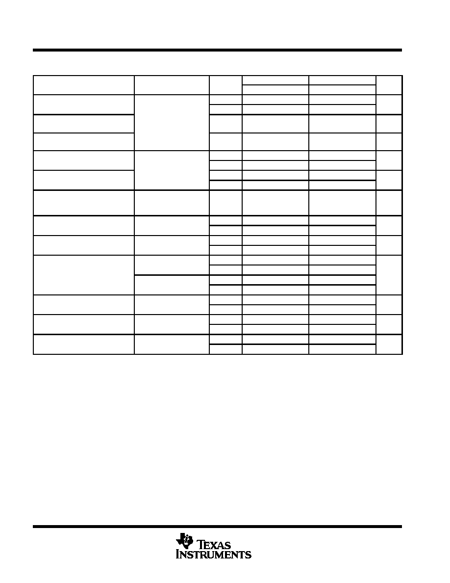
TLC220x, TLC220xA, TLC220xB, TLC220xY
Advanced LinCMOS
TM
LOW-NOISE PRECISION
OPERATIONAL AMPLIFIERS
SLOS175 ≠ FEBRUARY 1997
38
POST OFFICE BOX 655303
∑
DALLAS, TEXAS 75265
TLC2202M electrical characteristics at specified free-air temperature, V
DD
= 5 V (unless otherwise
noted)
PARAMETER
TEST CONDITIONS
T
TLC2202AM
TLC2202BM
UNIT
PARAMETER
TEST CONDITIONS
TA
MIN
TYP
MAX
MIN
TYP
MAX
UNIT
VIO
Input offset voltage
25
∞
C
80
500
80
500
µ
V
VIO
Input offset voltage
Full range
750
750
µ
V
VIO
Temperature coefficient of
VIC = 0
RS = 50
Full range
0 5
0 5
µ
V/
∞
C
VIO
input offset voltage
VIC = 0,
RS = 50
Full range
0.5
0.5
µ
V/
∞
C
Input offset voltage
long-term drift (see Note 4)
25
∞
C
0.001
0.005*
0.001
0.005*
µ
V/mo
IIO
Input offset current
25
∞
C
0.5
0.5
pA
IIO
Input offset current
VIC = 0
RS = 50
Full range
500
500
pA
IIB
Input bias current
VIC = 0,
RS = 50
25
∞
C
1
1
pA
IIB
Input bias current
Full range
500
500
pA
Common mode input
0
0
VICR
Common-mode input
voltage range
RS = 50
Full range
0
to
0
to
V
ICR
voltage range
S
g
2.7
2.7
VOH
Maximum high-level output
RL = 10 k
25
∞
C
4.7
4.8
4.7
4.8
V
VOH
g
voltage
RL = 10 k
Full range
4.7
4.7
V
VOL
Maximum low-level output
IO = 0
25
∞
C
0
50
0
50
mV
VOL
voltage
IO = 0
Full range
50
50
mV
VO = 1 V to 4 V,
25
∞
C
150
315
150
315
AVD
Large-signal differential
O
,
RL = 500 k
Full range
75
75
V/mV
AVD
g
g
voltage amplification
VO = 1 V to 4 V,
25
∞
C
25
55
25
55
V/mV
O
,
RL = 10 k
Full range
10
10
CMRR
Common-mode rejection
VO = 0, VIC = VICRmin,
25
∞
C
75
110
75
110
dB
CMRR
j
ratio
O
,
IC
ICR
,
RS = 50
Full range
75
75
dB
kSVR
Supply-voltage rejection
VDD = 4 6 V to 16 V
25
∞
C
80
110
80
110
dB
kSVR
y
g
j
ratio (
VDD
±
/
VIO)
VDD = 4.6 V to 16 V
Full range
80
80
dB
IDD
Supply current
VO = 2 5 V
No load
25
∞
C
1.7
2.6
1.7
2.6
mA
IDD
Supply current
VO = 2.5 V,
No load
Full range
2.6
2.6
mA
* On products compliant to MIL-PRF-38535, Class B, this parameter is not production tested.
Full range is ≠ 55
∞
C to 125
∞
C
NOTE 4: Typical values are based on the input offset voltage shift observed through 168 hours of operating life test at TA = 150
∞
C extrapolated
to TA = 25
∞
C using the Arrhenius equation and assuming an activation energy of 0.96 eV.

TLC220x, TLC220xA, TLC220xB, TLC220xY
Advanced LinCMOS
TM
LOW-NOISE PRECISION
OPERATIONAL AMPLIFIERS
SLOS175 ≠ FEBRUARY 1997
39
POST OFFICE BOX 655303
∑
DALLAS, TEXAS 75265
TLC2202M operating characteristics at specified free-air temperature, V
DD
= 5 V
PARAMETER
TEST CONDITIONS
T
TLC2202AM
TLC2202BM
UNIT
PARAMETER
TEST CONDITIONS
TA
MIN
TYP
MAX
MIN
TYP
MAX
UNIT
VO = 0 5 V to 2 5 V
25
∞
C
1 6
2 5
1 6
2 5
SR
Slew rate at unity gain
VO = 0.5 V to 2.5 V,
RL 10 k
25
∞
C
1.6
2.5
1.6
2.5
V/
µ
s
SR
Slew rate at unity gain
RL = 10 k
,
CL = 100 pF
Full range
0.9
1.1
V/
µ
s
V
Equivalent input noise voltage
f = 10 Hz
25
∞
C
18
35*
18
30*
nV/
Hz
Vn
q
g
(see Note 5)
f = 1 kHz
25
∞
C
8
15*
8
12*
nV/
Hz
VN(PP)
Peak-to-peak equivalent input
f = 0.1 to 1 Hz
25
∞
C
0.5
0.5
µ
V
VN(PP)
q
noise voltage
f = 0.1 to 10 Hz
25
∞
C
0.7
0.7
µ
V
In
Equivalent input noise current
25
∞
C
0.6
0.6
fA/
Hz
f = 10 kHz,
Gain-bandwidth product
,
RL = 10 k
,
25
∞
C
1.9
1.9
MHz
L
CL = 100 pF
Phase margin at unity gain
RL = 10 k
,
25
∞
C
47
∞
47
∞
m
Phase margin at unity gain
L
CL = 100 pF
25
∞
C
47
∞
47
∞
* On products compliant to MIL-PRF-38535, Class B, this parameter is not production tested.
Full range is ≠ 55
∞
C to 125
∞
C
NOTE 5: This parameter is tested on a sample basis for the TLC2202A and on all devices for the TLC2202B. For other test requirements, please
contact the factory. This statement has no bearing on testing or nontesting of other parameters.
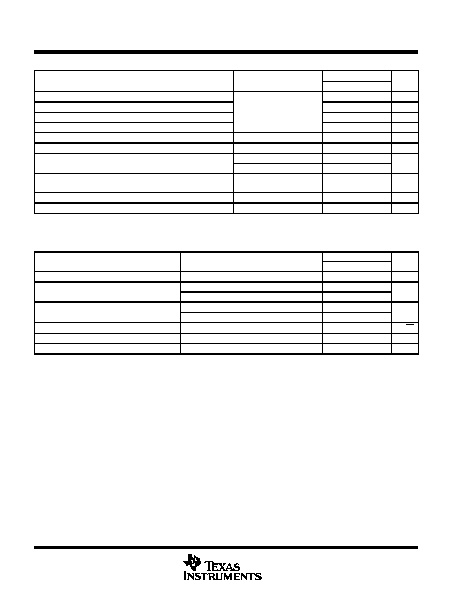
TLC220x, TLC220xA, TLC220xB, TLC220xY
Advanced LinCMOS
TM
LOW-NOISE PRECISION
OPERATIONAL AMPLIFIERS
SLOS175 ≠ FEBRUARY 1997
40
POST OFFICE BOX 655303
∑
DALLAS, TEXAS 75265
TLC2201Y electrical characteristics at V
DD
±
=
±
5 V, T
A
= 25
∞
C (unless otherwise noted)
PARAMETER
TEST CONDITIONS
TLC2201Y
UNIT
PARAMETER
TEST CONDITIONS
MIN
TYP
MAX
UNIT
VIO
Input offset voltage
100
µ
V
Input offset voltage long-term drift (see Note 4)
VIC = 0
RS = 50
0.001
µ
V/mo
IIO
Input offset current
VIC = 0,
RS = 50
0.5
pA
IIB
Input bias current
1
pA
VOH
Maximum high-level output voltage
RL = 10 k
4.8
V
VOL
Maximum low-level output voltage
IO = 0
0
mV
AVD
Large signal differential voltage amplification
VO = 1 V to 4 V, RL = 500
55
V/mV
AVD
Large-signal differential voltage amplification
VO = 1 V to 4 V, RL = 10
55
V/mV
CMRR
Common-mode rejection ratio
VIC = VICRmin,
RS = 50
VO = 0,
110
dB
kSVR
Supply voltage rejection ratio (
VDD
±
/
VIO)
VDD = 4.6 to 16 V
110
dB
IDD
Supply current per amplifier
VO = 2.5 V,
No load
1
mA
NOTE 4: Typical values are based on the input offset voltage shift observed through 168 hours of operating life test at TA = 150
∞
C extrapolated
to TA = 25
∞
C using the Arrhenius equation and assuming an activation energy of 0.96 eV.
TLC2201Y operating characteristics at V
DD
±
=
±
5 V, T
A
= 25
∞
C
PARAMETER
TEST CONDITIONS
TLC2201Y
UNIT
PARAMETER
TEST CONDITIONS
MIN
TYP
MAX
UNIT
SR
Positive slew rate at unity gain
VO =
±
0.5 to 2.5 V,
RL = 10 k
,
CL = 100 pF
2.5
V/
µ
s
V
Equivalent input noise voltage
f = 10 Hz
18
nV/
Hz
Vn
Equivalent input noise voltage
f = 1 kHz
8
nV/
Hz
VN(PP)
Peak-to-peak equivalent input noise
f = 0.1 to 1 Hz
0.5
µ
V
VN(PP)
q
voltage
f = 0.1 to 10 Hz
0.7
µ
V
In
Equivalent input noise current
0.6
pA/
Hz
Gain-bandwidth product
f = 10 kHz,
RL = 10 k
,
CL = 100 pF
1.8
MHz
m
Phase margin at unity gain
RL = 10 k
,
CL = 100 pF
48
∞

TLC220x, TLC220xA, TLC220xB, TLC220xY
Advanced LinCMOS
TM
LOW-NOISE PRECISION
OPERATIONAL AMPLIFIERS
SLOS175 ≠ FEBRUARY 1997
41
POST OFFICE BOX 655303
∑
DALLAS, TEXAS 75265
TLC2202Y electrical characteristics, V
DD
= 5 V, T
A
= 25
∞
C (unless otherwise noted)
PARAMETER
TEST CONDITIONS
TLC2202Y
UNIT
PARAMETER
TEST CONDITIONS
MIN
TYP
MAX
UNIT
VIO
Input offset voltage
100
µ
V
Input offset voltage long-term drift (see Note 4)
VIC = 0
RS = 50
0.001
µ
V/mo
IIO
Input offset current
VIC = 0,
RS = 50
0.5
pA
IIB
Input bias current
1
pA
VOH
Maximum high-level output voltage
RL = 10 k
4.8
V
VOL
Maximum low-level output voltage
IO = 0
0
mV
AVD
Large signal differential voltage amplification
VO = 1 V to 4 V,
RL = 500
315
V/mV
AVD
Large-signal differential voltage amplification
VO = 1 V to 4 V,
RL = 10
55
V/mV
CMRR
Common-mode rejection ratio
VO = 0, VICRmin,
RS = 50
110
dB
kSVR
Supply-voltage rejection ratio (
VDCC /
VIO)
VDD = 4.6 to 16 V
110
dB
IDD
Supply current
VO = 2.5 V,
No load
1.7
mA
NOTE 4: Typical values are based on the input offset voltage shift observed through 168 hours of operating life test at TA = 150
∞
C extrapolated
to TA = 25
∞
C using the Arrhenius equation and assuming an activation energy of 0.96 eV.
TLC2202Y operating characteristics at V
DD
= 5 V, T
A
= 25
∞
C
PARAMETER
TEST CONDITIONS
TLC2202Y
UNIT
PARAMETER
TEST CONDITIONS
MIN
TYP
MAX
UNIT
SR
Positive slew rate at unity gain
VO = 0.5 V to 2.5 V,
CL = 100 pF
RL = 10 k
,
2.5
V/
µ
s
V
Equivalent input noise voltage
f = 10 Hz
18
nV/
Hz
Vn
Equivalent input noise voltage
f = 10 kHz
8
nV/
Hz
VN(PP)
Peak to peak equivalent input noise voltage
f = 0.1 to 1 Hz
0.5
µ
V
VN(PP)
Peak-to-peak equivalent input noise voltage
f = 0.1 to 10 Hz
0.7
µ
V
In
Equivalent input noise current
0.6
pA/
Hz
B1
Gain-bandwidth product
f = 10 kHz,
CL = 100 pF
RL = 10 k
,
1.9
MHz
m
Phase margin at unity gain
RL = 10 k
,
CL = 100 pF
47
∞
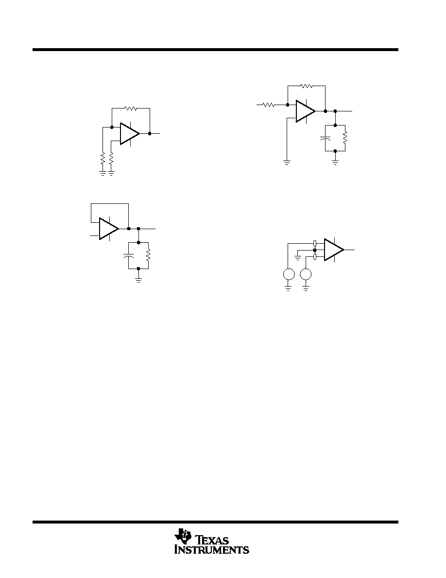
TLC220x, TLC220xA, TLC220xB, TLC220xY
Advanced LinCMOS
TM
LOW-NOISE PRECISION
OPERATIONAL AMPLIFIERS
SLOS175 ≠ FEBRUARY 1997
42
POST OFFICE BOX 655303
∑
DALLAS, TEXAS 75265
PARAMETER MEASUREMENT INFORMATION
Figure 1. Noise-Voltage Test Circuit
2 k
VDD +
VDD ≠ /GND
VO
20
20
≠
+
Figure 2. Phase-Margin Test Circuit
10 k
VDD +
VDD ≠
VO
100
≠
+
VI
CL
RL
(see Note A)
NOTE A: CL includes fixture capacitance.
Figure 3. Slew-Rate Test Circuit
VDD +
VDD ≠
VO
≠
+
CL
RL
(see Note A)
VI
NOTE A: CL includes fixture capacitance.
Figure 4. Input-Bias and Offset-Current Test Circuit
VDD +
VDD ≠ /GND
VO
≠
+
Ground Shield
pA
pA
typical values
Typical values presented in this data sheet represent the median (50% point) of device parametric performance.
input bias and offset current
At the picoamp bias current level of the TLC220x, TLC220xA, and TLC220xB, accurate measurement of the
bias current becomes difficult. Not only does this measurement require a picoammeter, but test socket leakages
can easily exceed the actual device bias currents. To measure these small currents, Texas Instruments uses
a two-step process. The socket leakage is measured using picoammeters with bias voltages applied but with
no device in the socket. The device is then inserted in the socket, and a second test measuring both the socket
leakage and the device input bias current is performed. The two measurements are then subtracted
algebraically to determine the bias current of the device.
noise
Texas Instruments offers automated production noise testing to meet individual application requirements. Noise
voltage at f = 10 Hz and f = 1 kHz is 100% tested on every TLC2201B device, while lot sample testing is
performed on the TLC220xA. For other noise requirements, please contact the factory.

TLC220x, TLC220xA, TLC220xB, TLC220xY
Advanced LinCMOS
TM
LOW-NOISE PRECISION
OPERATIONAL AMPLIFIERS
SLOS175 ≠ FEBRUARY 1997
43
POST OFFICE BOX 655303
∑
DALLAS, TEXAS 75265
TYPICAL CHARACTERISTICS
Table of Graphs
FIGURE
VIO
Input offset voltage
Distribution
5, 6
IIB
Input bias current
vs Common-mode input voltage
7
IIB
Input bias current
g
vs Free-air temperature
8
VOM
Maximum peak output voltage
vs Output current
9
VOM
Maximum peak output voltage
vs Free-air temperature
10
VO(PP) Maximum peak-to-peak output voltage
vs Frequency
11
vs Frequency
12
VOH
High-level output voltage
q
y
vs High-level output current
13
OH
g
g
g
vs Free-air temperature
14
VOL
Low level output voltage
vs Low-level output current
15
VOL
Low-level output voltage
vs Free-air temperature
16
AVD
Large signal differential voltage amplification
vs Frequency
17
AVD
Large-signal differential voltage amplification
q
y
vs Free-air temperature
18
IOS
Short circuit output current
vs Supply voltage
19
IOS
Short-circuit output current
y
g
vs Free-air temperature
20
CMRR
Common-mode rejection ratio
vs Frequency
21
IDD
Supply current
vs Supply voltage
22
IDD
Supply current
y
g
vs Free-air temperature
23, 24
Pulse response
Small signal
25, 26
Pulse response
g
Large signal
,
27, 28
SR
Slew rate
vs Supply voltage
29
SR
Slew rate
y
g
vs Free-air temperature
30
Noise voltage (referred to input)
0.1 to 1 Hz
31
Noise voltage (referred to input)
0.1 to 10 Hz
32
Gain bandwidth product
vs Supply voltage
33, 34
Gain-bandwidth product
y
g
vs Free-air temperature
,
35
Phase margin
vs Supply voltage
36, 37
m
Phase margin
y
g
vs Free-air temperature
,
38, 39
Phase shift
vs Frequency
17

TLC220x, TLC220xA, TLC220xB, TLC220xY
Advanced LinCMOS
TM
LOW-NOISE PRECISION
OPERATIONAL AMPLIFIERS
SLOS175 ≠ FEBRUARY 1997
44
POST OFFICE BOX 655303
∑
DALLAS, TEXAS 75265
TYPICAL CHARACTERISTICS
≠ 500
≠ 300
≠ 100
VIO ≠ Input Offset Voltage ≠
µ
V
12
8
4
0
100
Percentage of Units ≠ %
16
20
300
500
DISTRIBUTION OF TLC2201
INPUT OFFSET VOLTAGE
408 Units Tested From 2 Wafer Lots
VDD
±
=
±
5 V
TA = 25
∞
C
P Package
Figure 5
Figure 6
8
6
2
0
≠1000
200
Percentage of Units ≠ %
10
14
16
600
1000
4
12
TLC2202
DISTRIBUTION OF
INPUT OFFSET VOLTAGE
VIO ≠ Input Offset Voltage ≠
µ
V
VDD
±
=
±
15 V
1726 Amplifiers Tested From 1 Wafer Lot
≠ 600
≠ 200
TA = 25
∞
C
P Package
Figure 7
≠ 5
0
8
IIB ≠ Input Bias Current ≠ pA
4
2
6
INPUT BIAS CURRENT
vs
COMMON-MODE INPUT VOLTAGE
10
≠ 2
≠ 4
≠ 6
≠ 8
≠ 10
≠ 4
≠ 3
≠ 2
≠ 1
0
1
2
3
4
5
VIC ≠ Common-Mode Input Voltage ≠ V
I IB
VDD
±
=
±
5 V
TA = 25
∞
C
Figure 8
150
100
50
0
25
45
65
85
200
250
300
105
125
INPUT BIAS CURRENT
vs
FREE-AIR TEMPERATURE
≠ Input Bias Current ≠ pA
I IB
TA ≠ Free-Air Temperature ≠
∞
C
VO = 0
VIC = 0
VDD
±
=
±
5 V
Data at high and low temperatures are applicable only within the rated operating free-air temperature ranges of the various devices.
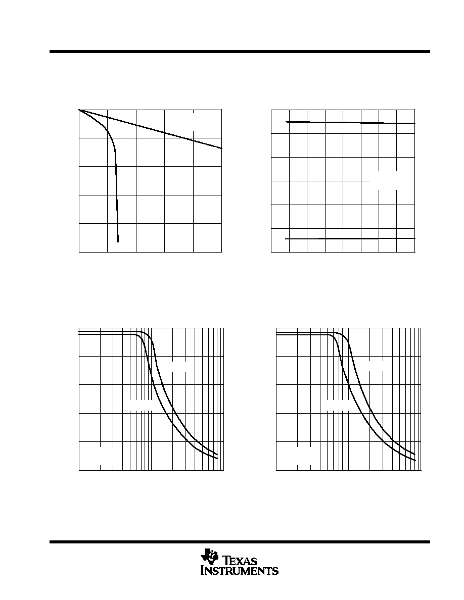
TLC220x, TLC220xA, TLC220xB, TLC220xY
Advanced LinCMOS
TM
LOW-NOISE PRECISION
OPERATIONAL AMPLIFIERS
SLOS175 ≠ FEBRUARY 1997
45
POST OFFICE BOX 655303
∑
DALLAS, TEXAS 75265
TYPICAL CHARACTERISTICS
Figure 9
3
2
1
0
0
2
4
6
VOM | ≠ Maximum Peak Output V
oltage ≠ V
4
5
8
10
|V
OM
MAXIMUM PEAK OUTPUT VOLTAGE
vs
OUTPUT CURRENT
|IO| ≠ Output Current ≠ mA
VOM ≠
VDD
±
=
±
5 V
TA = 25
∞
C
VOM +
Figure 10
4
MAXIMUM PEAK OUTPUT VOLTAGE
vs
FREE-AIR TEMPERATURE
TA ≠ Free-Air Temperature ≠
∞
C
VOM ≠ Maximum Peak Output V
oltage ≠ V
V
OM
VDD
±
=
±
5 V
RL = 10 k
6
2
0
≠ 2
≠ 4
≠ 6
≠ 75
≠ 50
≠ 25
0
25
50
75
100
125
VOM ≠
VOM +
Figure 11
2
0
10
10 k
100 k
1 M
≠ Maximum Peak-to-Peak Output V
oltage ≠ V
f ≠ Frequency ≠ Hz
8
6
4
V
O(PP)
MAXIMUM PEAK-TO-PEAK OUTPUT VOLTAGE
vs
FREQUENCY
VDD
±
=
±
5 V
RL = 10 k
TA = ≠ 55
∞
C
30 k
300 k
TA = 125
∞
C
Figure 12
1
0
5
10 k
100 k
1 M
V0H ≠ High-Level Output V
oltage ≠ V
f ≠ Frequency ≠ Hz
4
3
2
HIGH-LEVEL OUTPUT VOLTAGE
vs
FREQUENCY
VDD = 5 V
RL = 10 k
TA = ≠ 55
∞
C
V
OH
30 k
300 k
TA = 125
∞
C
Data at high and low temperatures are applicable only within the rated operating free-air temperature ranges of the various devices.
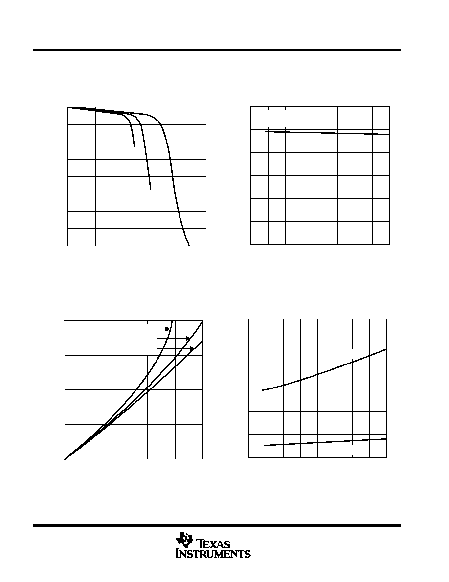
TLC220x, TLC220xA, TLC220xB, TLC220xY
Advanced LinCMOS
TM
LOW-NOISE PRECISION
OPERATIONAL AMPLIFIERS
SLOS175 ≠ FEBRUARY 1997
46
POST OFFICE BOX 655303
∑
DALLAS, TEXAS 75265
TYPICAL CHARACTERISTICS
Figure 13
0
1
2
3
4
5
VDD ≠ 6
VOM ≠ High-Level Output V
oltage ≠ V
V
OH
VDD ≠ 8
VDD ≠ 10
VDD ≠ 12
VDD ≠ 14
VDD ≠ 16
VDD
VDD ≠ 2
VDD ≠ 4
IOH ≠ High-Level Output Current ≠ mA
VDD = 5 V
VDD = 10 V
VDD = 16 V
HIGH-LEVEL OUTPUT VOLTAGE
vs
HIGH-LEVEL OUTPUT CURRENT
TA = 25
∞
C
Figure 14
1
2
5
TA ≠ Free-Air Temperature ≠
∞
C
6
4
3
0
≠ 75
≠ 50
≠ 25
0
25
50
75
100
125
HIGH-LEVEL OUTPUT VOLTAGE
vs
FREE-AIR TEMPERATURE
TA ≠ Free-Air Temperature ≠
∞
C
VDD = 5 V
RL = 10 k
VOM ≠ High-Level Output V
oltage ≠ V
V
OH
Figure 15
VOL
≠ Low-Level Output V
oltage ≠ V
1.5
1
0.5
0
0
2
4
6
2
8
10
TA = 25
∞
C
IOL ≠ Low-Level Output Current ≠ mA
V
OL
LOW-LEVEL OUTPUT VOLTAGE
vs
LOW-LEVEL OUTPUT CURRENT
VDD = 5 V
VDD = 10 V
VDD = 16 V
Figure 16
≠ 75
≠ 50
≠ 25
0
25
50
75
100
125
VOL
≠ Low-Level Output V
oltage ≠ V
1
0.5
0
1.5
TA ≠ Free-Air Temperature ≠
∞
C
V
OL
VDD = 5 V
LOW-LEVEL OUTPUT VOLTAGE
vs
FREE-AIR TEMPERATURE
IOL = 5 mA
IOL = 1 mA
Data at high and low temperatures are applicable only within the rated operating free-air temperature ranges of the various devices.

TLC220x, TLC220xA, TLC220xB, TLC220xY
Advanced LinCMOS
TM
LOW-NOISE PRECISION
OPERATIONAL AMPLIFIERS
SLOS175 ≠ FEBRUARY 1997
47
POST OFFICE BOX 655303
∑
DALLAS, TEXAS 75265
TYPICAL CHARACTERISTICS
LARGE-SIGNAL DIFFERENTIAL VOLTAGE
AMPLIFICATION
vs
FREE-AIR TEMPERATURE
≠ 75
≠ 50
≠ 25
0
25
50
75
100
125
80
90
100
110
120
130
TA ≠ Free-Air Temperature ≠
∞
C
VDD
±
=
±
5 V, RL = 500 k
VDD = 5 V, RL = 500 k
VDD
±
=
±
5 V, RL = 10 k
VDD = 5 V, RL = 10 k
A
VD ≠ Large-Signal Differential
¡¡
¡¡
¡¡
A
VD
V
oltage
Amplification ≠ dB
10
100
1 k
10 k
f ≠ Frequency ≠ Hz
LARGE-SIGNAL DIFFERENTIAL VOLTAGE
AMPLIFICATION AND PHASE SHIFT
vs
FREQUENCY
100 k
1 M
≠ 20
0
20
40
60
80
100
120
170
∞
150
∞
130
∞
110
∞
90
∞
70
∞
50
∞
30
∞
Phase Shift
AVD
Phase Shift
VDD
±
=
±
5 V
RL = 10 k
CL = 100 pF
TA = 25
∞
C
A
VD ≠ Large-Signal Differential
¡¡
¡¡
A
VD
V
oltage
Amplification ≠ dB
Figure 17
Figure 18
Figure 19
0
1
2
3
4
5
6
7
8
≠ 12
≠ 8
≠ 4
0
4
8
|VDD
±
| ≠ Supply Voltage ≠ V
12
SHORT-CIRCUIT OUTPUT CURRENT
vs
SUPPLY VOLTAGE
VID = ≠ 100 mV
IOS ≠ Short-Circuit Output Current ≠ mA OS
I
VO = 0
TA= 25
∞
C
VID = 100 mV
Figure 20
≠ 15
SHORT-CIRCUIT OUTPUT CURRENT
vs
FREE-AIR TEMPERATURE
≠ 75
≠ 50
≠ 25
0
25
50
75
100
125
≠ 10
≠ 5
0
5
10
15
TA ≠ Free-Air Temperature ≠
∞
C
VID = 100 mV
VID = ≠ 100 mV
VDD
±
=
±
5 V
VO = 0
IOS ≠ Short-Circuit Output Current ≠ mA OS
I
Data at high and low temperatures are applicable only within the rated operating free-air temperature ranges of the various devices.
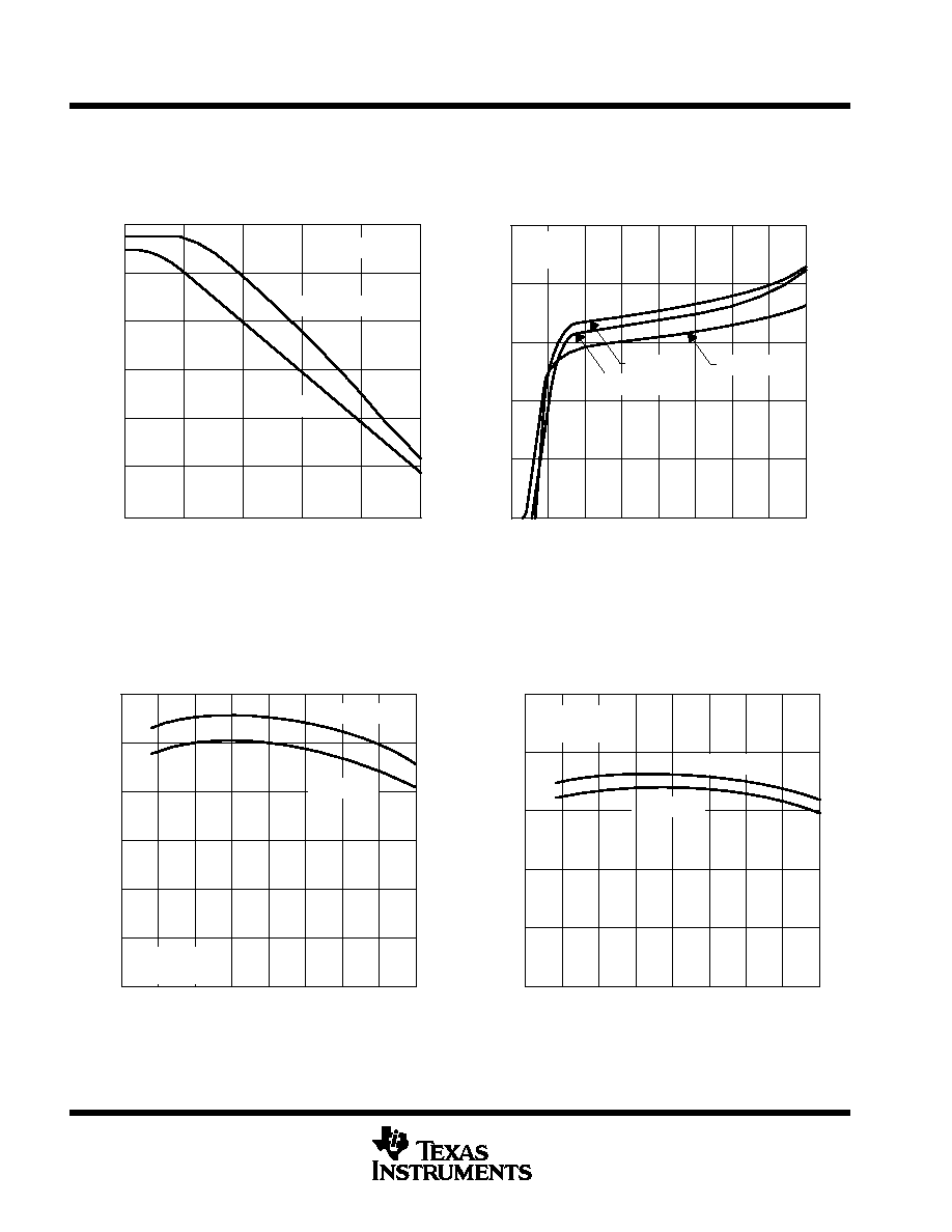
TLC220x, TLC220xA, TLC220xB, TLC220xY
Advanced LinCMOS
TM
LOW-NOISE PRECISION
OPERATIONAL AMPLIFIERS
SLOS175 ≠ FEBRUARY 1997
48
POST OFFICE BOX 655303
∑
DALLAS, TEXAS 75265
TYPICAL CHARACTERISTICS
Figure 21
60
40
20
0
10
100
1 k
10 k
CMRR ≠ Common-Mode Rejection Ratio ≠ dB
80
100
120
100 k
1 M
COMMON-MODE REJECTION RATIO
vs
FREQUENCY
f ≠ Frequency ≠ Hz
TA = 25
∞
C
VDD
±
=
±
5 V
VDD = 5 V
Figure 22
1.5
1
0.5
0
0
1
2
3
4
5
2
2.5
6
7
8
IDD ≠ Supply Current ≠ mA DD
I
|VDD
±
| ≠ Supply Voltage ≠ V
VO = 0
No Load
TA = 25
∞
C
TA = 125
∞
C
SUPPLY CURRENT
vs
SUPPLY VOLTAGE
TA = ≠ 55
∞
C
Figure 23
≠ 75
≠ 50
≠ 25
0
25
50
75
100
125
0
0.2
0.4
0.6
0.8
1
1.2
TA ≠ Free-Air Temperature ≠
∞
C
IDD ≠ Supply Current ≠ mA DD
I
VO = VDD + / 2
No Load
VDD = 5 V
VDD
±
=
±
5 V
TLC2201
SUPPLY CURRENT
vs
FREE-AIR TEMPERATURE
Figure 24
≠ 75
≠ 50
≠ 25
0
25
50
75
100
125
TA ≠ Free-Air Temperature ≠
∞
C
1.5
1
0.5
0
2
2.5
IDD ≠ Supply Current ≠ mA DD
I
VO = VDD + /2
No Load
VDD = 5 V
VDD
±
=
±
5 V
TLC2202
SUPPLY CURRENT
vs
FREE-AIR TEMPERATURE
Data at high and low temperatures are applicable only within the rated operating free-air temperature ranges of the various devices.
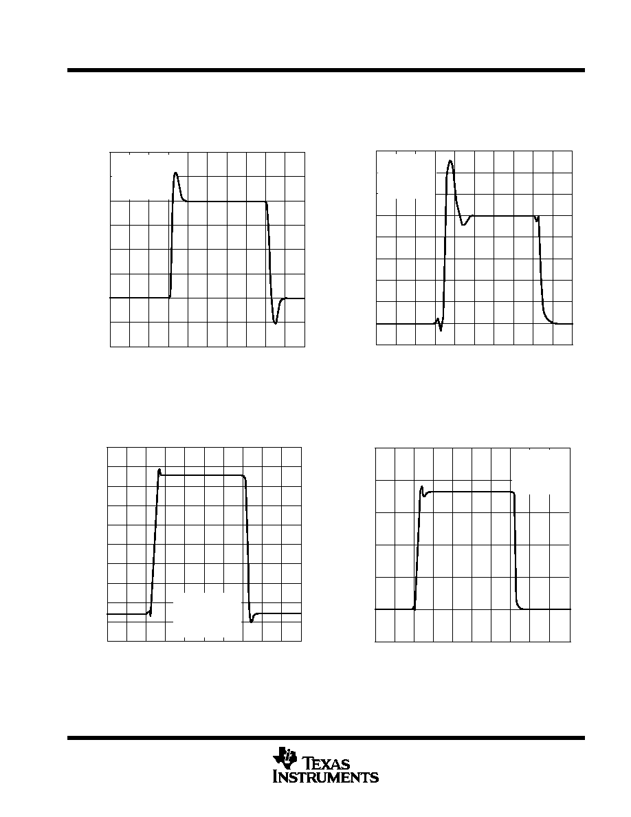
TLC220x, TLC220xA, TLC220xB, TLC220xY
Advanced LinCMOS
TM
LOW-NOISE PRECISION
OPERATIONAL AMPLIFIERS
SLOS175 ≠ FEBRUARY 1997
49
POST OFFICE BOX 655303
∑
DALLAS, TEXAS 75265
TYPICAL CHARACTERISTICS
Figure 25
VOLTAGE-FOLLOWER
SMALL-SIGNAL
PULSE RESPONSE
VO ≠ Output V
oltage
≠
mV
0
≠75
≠100
0
1
2
3
25
75
100
4
5
6
7
50
t ≠ Time ≠
µ
s
V
O
VDD
±
=
±
5 V
RL = 10 k
CL = 100 pF
TA = 25
∞
C
≠ 25
≠ 50
Figure 26
VOLTAGE-FOLLOWER
SMALL-SIGNAL
PULSE RESPONSE
80
60
20
0
160
40
0
1
2
3
120
100
140
4
5
6
7
VO ≠ Output V
oltage
≠
mV
V
O
t ≠ Time ≠
µ
s
VDD = 5 V
RL = 10 k
CL = 100 pF
TA = 25
∞
C
≠ 20
Figure 27
0
4
0
5
10
15
20
2
1
3
5
25
30
35
40
VO ≠ Output V
oltage
≠
V
V
O
t ≠ Time ≠
µ
s
VOLTAGE-FOLLOWER
LARGE-SIGNAL
PULSE RESPONSE
VDD
±
=
±
5 V
RL = 10 k
CL = 100 pF
TA = 25
∞
C
≠ 1
≠ 2
≠ 3
≠ 4
≠ 5
Figure 28
VO ≠ Output V
oltage
≠
V
V
O
VOLTAGE-FOLLOWER
LARGE-SIGNAL
PULSE RESPONSE
2
1
0
≠1
0
5
10
15
20
3
4
5
25
30
35
40
t ≠ Time ≠
µ
s
VDD = 5 V
RL = 10 k
CL = 100 pF
TA = 25
∞
C

TLC220x, TLC220xA, TLC220xB, TLC220xY
Advanced LinCMOS
TM
LOW-NOISE PRECISION
OPERATIONAL AMPLIFIERS
SLOS175 ≠ FEBRUARY 1997
50
POST OFFICE BOX 655303
∑
DALLAS, TEXAS 75265
TYPICAL CHARACTERISTICS
Figure 29
2
1
0
0
1
2
3
4
5
3
4
6
7
8
SLEW RATE
vs
SUPPLY VOLTAGE
|VDD
±
| ≠ Supply Voltage ≠ V
RL = 10 k
CL = 100 pF
TA = 25
∞
C
SR ≠
SR +
µ
s
SR ≠ Slew Rate ≠ V/
Figure 30
µ
s
SR ≠ Slew Rate ≠ V/
≠ 75
≠ 50
≠ 25
0
25
50
75
100
125
0
1
2
3
TA ≠ Free-Air Temperature ≠
∞
C
SLEW RATE
vs
FREE-AIR TEMPERATURE
VDD
±
=
±
5 V
RL = 10 k
CL = 100 pF
SR +
SR ≠
4
Figure 31
NOISE VOLTAGE
(REFERRED TO INPUT)
OVER A 10-SECOND INTERVAL
Noise V
oltage ≠ uV
0
≠1
0
1
2
3
4
5
6
0.25
0.75
t ≠ Time ≠ s
1
7
8
9
10
0.5
VDD
±
=
±
5 V
f = 0.1 Hz to 1 Hz
TA= 25
∞
C
V
µ
≠ 0.25
≠ 0.5
≠ 0.75
Figure 32
0
≠1
0.8
0
1
2
3
4
5
6
0.4
0.2
0.6
t ≠ Time ≠ s
1
7
8
9
10
NOISE VOLTAGE
(REFERRED TO INPUT)
OVER A 10-SECOND INTERVAL
VDD
±
=
±
5 V
f = 0.1 Hz to 10 Hz
TA= 25
∞
C
Noise V
oltage ≠ uV
V
µ
≠ 0.2
≠ 0.4
≠ 0.6
≠ 0.8
Data at high and low temperatures are applicable only within the rated operating free-air temperature ranges of the various devices.
TLC220x, TLC220xA, TLC220xB, TLC220xY
Advanced LinCMOS
TM
LOW-NOISE PRECISION
OPERATIONAL AMPLIFIERS
SLOS175 ≠ FEBRUARY 1997
51
POST OFFICE BOX 655303
∑
DALLAS, TEXAS 75265
TYPICAL CHARACTERISTICS
Figure 33
1.9
1.8
0
1
2
3
4
5
Gain-Bandwidth Product ≠ MHz
2
2.1
6
7
8
|VDD
±
| ≠ Supply Voltage ≠ V
RL = 10 k
CL = 100 pF
TA = 25
∞
C
TLC2201
GAIN-BANDWIDTH PRODUCT
vs
SUPPLY VOLTAGE
Figure 34
1.9
1.8
0
1
2
3
4
5
Gain-Bandwidth Product ≠ MHz
2
2.1
6
7
8
|VDD
±
| ≠ Supply Voltage ≠ V
f = 10 kHz
RL = 10 k
CL = 100 pF
TA = 25
∞
C
TLC2202
GAIN-BANDWIDTH PRODUCT
vs
SUPPLY VOLTAGE
Figure 35
≠ 75
≠ 50
≠ 25
0
25
50
75
100
125
1
1.5
2
2.5
TA ≠ Free-Air Temperature ≠
∞
C
Gain-Bandwidth Product ≠ MHz
GAIN-BANDWIDTH PRODUCT
vs
FREE-AIR TEMPERATURE
f = 10 kHz
RL = 10 k
CL = 100 pF
VDD
±
=
±
5 V
VDD = 5 V
Figure 36
0
1
2
3
4
5
6
7
8
|VDD
±
| ≠ Supply Voltage ≠ V
RL = 10 k
CL = 100 pF
TA = 25
∞
C
om ≠ Phase Margin
m
50
∞
48
∞
46
∞
44
∞
42
∞
40
∞
TLC2201
PHASE MARGIN
vs
SUPPLY VOLTAGE
Data at high and low temperatures are applicable only within the rated operating free-air temperature ranges of the various devices.
TLC220x, TLC220xA, TLC220xB, TLC220xY
Advanced LinCMOS
TM
LOW-NOISE PRECISION
OPERATIONAL AMPLIFIERS
SLOS175 ≠ FEBRUARY 1997
52
POST OFFICE BOX 655303
∑
DALLAS, TEXAS 75265
TYPICAL CHARACTERISTICS
Figure 37
50
∞
48
∞
46
∞
44
∞
42
∞
40
∞
0
1
2
3
4
5
6
7
8
|VDD
±
| ≠ Supply Voltage ≠ V
RL = 10 k
CL = 100 pF
TA = 25
∞
C
om ≠ Phase Margin
m
TLC2202
PHASE MARGIN
vs
SUPPLY VOLTAGE
Figure 38
≠ 75
≠ 50
≠ 25
0
25
50
75
100
125
TA ≠ Free-Air Temperature ≠
∞
C
VDD
±
=
±
5 V
VDD = 5 V
RL = 10 k
CL = 100 pF
50
∞
48
∞
46
∞
44
∞
42
∞
40
∞
om ≠ Phase Margin
m
TLC2201
PHASE MARGIN
vs
FREE-AIR TEMPERATURE
Figure 39
50
∞
48
∞
46
∞
44
∞
42
∞
40
∞
≠ 75
≠ 50
≠ 25
0
25
50
75
100
125
TA ≠ Free-Air Temperature ≠
∞
C
VDD
±
=
±
5 V
VDD = 5 V
RL = 10 k
CL = 100 pF
om ≠ Phase Margin
m
TLC2202
PHASE MARGIN
vs
FREE-AIR TEMPERATURE
Data at high and low temperatures are applicable only within the rated operating free-air temperature ranges of the various devices.

TLC220x, TLC220xA, TLC220xB, TLC220xY
Advanced LinCMOS
TM
LOW-NOISE PRECISION
OPERATIONAL AMPLIFIERS
SLOS175 ≠ FEBRUARY 1997
53
POST OFFICE BOX 655303
∑
DALLAS, TEXAS 75265
APPLICATION INFORMATION
latch-up avoidance
Because CMOS devices are susceptible to latch-up due to their inherent parasitic thyristors, the TLC220x,
TLC220xA, and TLC220xB inputs and outputs are designed to withstand ≠ 100-mA surge currents without
sustaining latch-up; however, techniques reducing the chance of latch-up should be used whenever possible.
Internal protection diodes should not be forward biased in normal operation. Applied input and output voltages
should not exceed the supply voltage by more than 300 mV. Care should be exercised when using capacitive
coupling on pulse generators. Supply transients should be shunted by the use of decoupling capacitors
(0.1
µ
F typical) located across the supply rails as close to the device as possible.
electrostatic discharge protection
These devices use internal ESD-protection circuits that prevent functional failures at voltages at or below
2000 V. Care should be exercised in handling these devices as exposure to ESD may result in degradation of
the device parametric performance.
macromodel information
Macromodel information provided was derived using Microsim
Parts
TM
, the model generation software used
with Microsim
PSpice
TM
. The Boyle macromodel (see Note 5) and subcircuit in Figure 40 were generated using
the TLC220x typical electrical and operating characteristics at 25
∞
C. Using this information, output simulations
of the following key parameters can be generated to a tolerance of 20% (in most cases):
D
Unity-gain frequency
D
Common-mode rejection ratio
D
Phase margin
D
DC output resistance
D
AC output resistance
D
Short-circuit output current limit
D
Maximum positive output voltage swing
D
Maximum negative output voltage swing
D
Slew rate
D
Quiescent power dissipation
D
Input bias current
D
Open-loop voltage amplification
NOTE 5: G. R. Boyle, B. M. Cohn, D. O. Pederson, and J. E. Solomon, "Macromodeling of Integrated Circuit Operational Amplifiers",
IEEE Journal
of Solid-State Circuits, SC-9, 353 (1974).
PSpice and Parts are trademarks of MicroSim Corporation.
TLC220x, TLC220xA, TLC220xB, TLC220xY
Advanced LinCMOS
TM
LOW-NOISE PRECISION
OPERATIONAL AMPLIFIERS
SLOS175 ≠ FEBRUARY 1997
54
POST OFFICE BOX 655303
∑
DALLAS, TEXAS 75265
APPLICATION INFORMATION
macromodel information (continued)
OUT
+
≠
+
≠
+
≠
+
≠
+
≠
+
≠
+
≠
+
≠
.subckt TLC220x 1 2 3 4 5
*
c1
11
12 8.51E≠12
c2
6
7
50.00E≠12
cpsr 85
86 79.6E≠9
dcm+ 81
82 dx
dcm≠ 83
81 dx
dc
5
53 dx
de
54
5
dx
dlp
90
91 dx
dln
92
90 dx
dp
4
3
dx
ecmr 84
99 (2,99) 1
egnd 99
0
poly(2) (3,0) (4,0) 0 .5 .5
epsr 85
0
poly(1) (3,4) ≠200E≠6 20E≠6
ense 89
2
poly(1) (88,0) 100E≠6 1
fb
7
99 poly(6) vb vc ve vlp vln
+ vpsr 0 +
895.9E3 ≠90E3 90E3 90E3 ≠90E3 895E3
ga
6
0
11 12 314.2E≠6
gcm
0
6
10 99 1.295E≠9
gpsr 85
86 (85,86) 100E≠6
grd1 60
11 (60,11) 3.141E≠4
grd2 60
12 (60,12) 3.141E≠4
hlim 90
0
vlim 1k
hcmr 80
1
poly(2) vcm+ vcm≠ 0 1E2 1E2
irp
3
4
965E≠6
VCC +
rp
IN ≠
2
IN+
1
VCC ≠
rd1
11
j1
j2
10
rss
iss
3
12
rd2
ve
54
de
dp
vc
dc
4
C1
53
r2
6
9
egnd
vb
fb
C2
gcm
ga
vlim
8
5
ro1
ro2
hlim
90
dip
91
din
92
vin
vip
99
7
iss
3
10 dc 135.0E≠6
iio
2
0
.5E≠12
i1
88
0
1E≠21
j1
11
89 10 jx
j2
12
80 10 jx
r2
6
9
100.0E3
rcm
84
81 1k
rn1
88
0
1500
ro1
8
5
188
ro2
7
99 187
rss
10
99 1.481E6
vad
60
4
≠.3v
vcm+ 82
99 2.2
vcm≠ 83
99 ≠4.5
vb
9
0
dc 0
vc
3
53 dc .9
ve
54
4
dc .8
vlim 7
8
dc 0
vlp
91
0
dc 2.8
vln
0
92 dc 2.8
vpsr 0
86 dc 0
.model dx
d(is=800.0E≠18)
.model jx pjf(is=500.0E≠15 beta=1.462E≠3
+ vto=≠.155 kf=1E≠17)
.endsx
Figure 40. Boyle Macromodel and Subcircuit

TLC220x, TLC220xA, TLC220xB, TLC220xY
Advanced LinCMOS
TM
LOW-NOISE PRECISION
OPERATIONAL AMPLIFIERS
SLOS175 ≠ FEBRUARY 1997
55
POST OFFICE BOX 655303
∑
DALLAS, TEXAS 75265
MECHANICAL INFORMATION
D (R-PDSO-G**)
PLASTIC SMALL-OUTLINE PACKAGE
14 PIN SHOWN
4040047 / B 03/95
0.228 (5,80)
0.244 (6,20)
0.069 (1,75) MAX
0.010 (0,25)
0.004 (0,10)
1
14
0.014 (0,35)
0.020 (0,51)
A
0.157 (4,00)
0.150 (3,81)
7
8
0.044 (1,12)
0.016 (0,40)
Seating Plane
0.010 (0,25)
PINS **
0.008 (0,20) NOM
A MIN
A MAX
DIM
Gage Plane
0.189
(4,80)
(5,00)
0.197
8
(8,55)
(8,75)
0.337
14
0.344
(9,80)
16
0.394
(10,00)
0.386
0.004 (0,10)
M
0.010 (0,25)
0.050 (1,27)
0
∞
≠ 8
∞
NOTES: A. All linear dimensions are in inches (millimeters).
B. This drawing is subject to change without notice.
C. Body dimensions do not include mold flash or protrusion, not to exceed 0.006 (0,15).
D. Four center pins are connected to die mount pad.
E. Falls within JEDEC MS-012
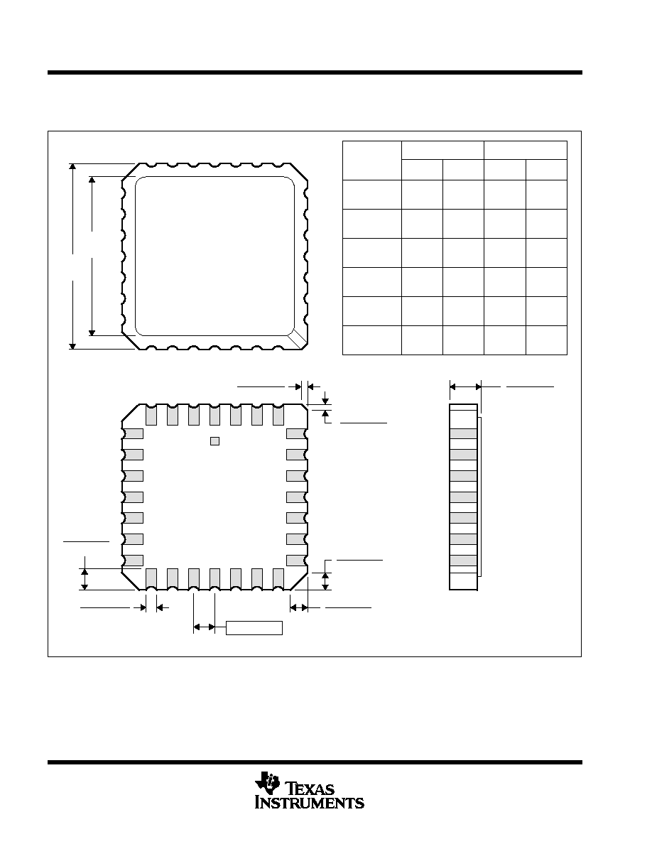
TLC220x, TLC220xA, TLC220xB, TLC220xY
Advanced LinCMOS
TM
LOW-NOISE PRECISION
OPERATIONAL AMPLIFIERS
SLOS175 ≠ FEBRUARY 1997
56
POST OFFICE BOX 655303
∑
DALLAS, TEXAS 75265
MECHANICAL INFORMATION
FK (S-CQCC-N**)
LEADLESS CERAMIC CHIP CARRIER
4040140 / D 10/96
28 TERMINAL SHOWN
B
0.358
(9,09)
MAX
(11,63)
0.560
(14,22)
0.560
0.458
0.858
(21,8)
1.063
(27,0)
(14,22)
A
NO. OF
MIN
MAX
0.358
0.660
0.761
0.458
0.342
(8,69)
MIN
(11,23)
(16,26)
0.640
0.739
0.442
(9,09)
(11,63)
(16,76)
0.962
1.165
(23,83)
0.938
(28,99)
1.141
(24,43)
(29,59)
(19,32)
(18,78)
**
20
28
52
44
68
84
0.020 (0,51)
TERMINALS
0.080 (2,03)
0.064 (1,63)
(7,80)
0.307
(10,31)
0.406
(12,58)
0.495
(12,58)
0.495
(21,6)
0.850
(26,6)
1.047
0.045 (1,14)
0.045 (1,14)
0.035 (0,89)
0.035 (0,89)
0.010 (0,25)
12
13
14
15
16
18
17
11
10
8
9
7
5
4
3
2
0.020 (0,51)
0.010 (0,25)
6
1
28
26
27
19
21
B SQ
A SQ
22
23
24
25
20
0.055 (1,40)
0.045 (1,14)
0.028 (0,71)
0.022 (0,54)
0.050 (1,27)
NOTES: A. All linear dimensions are in inches (millimeters).
B. This drawing is subject to change without notice.
C. This package can be hermetically sealed with a metal lid.
D. The terminals are gold plated.
E. Falls within JEDEC MS-004
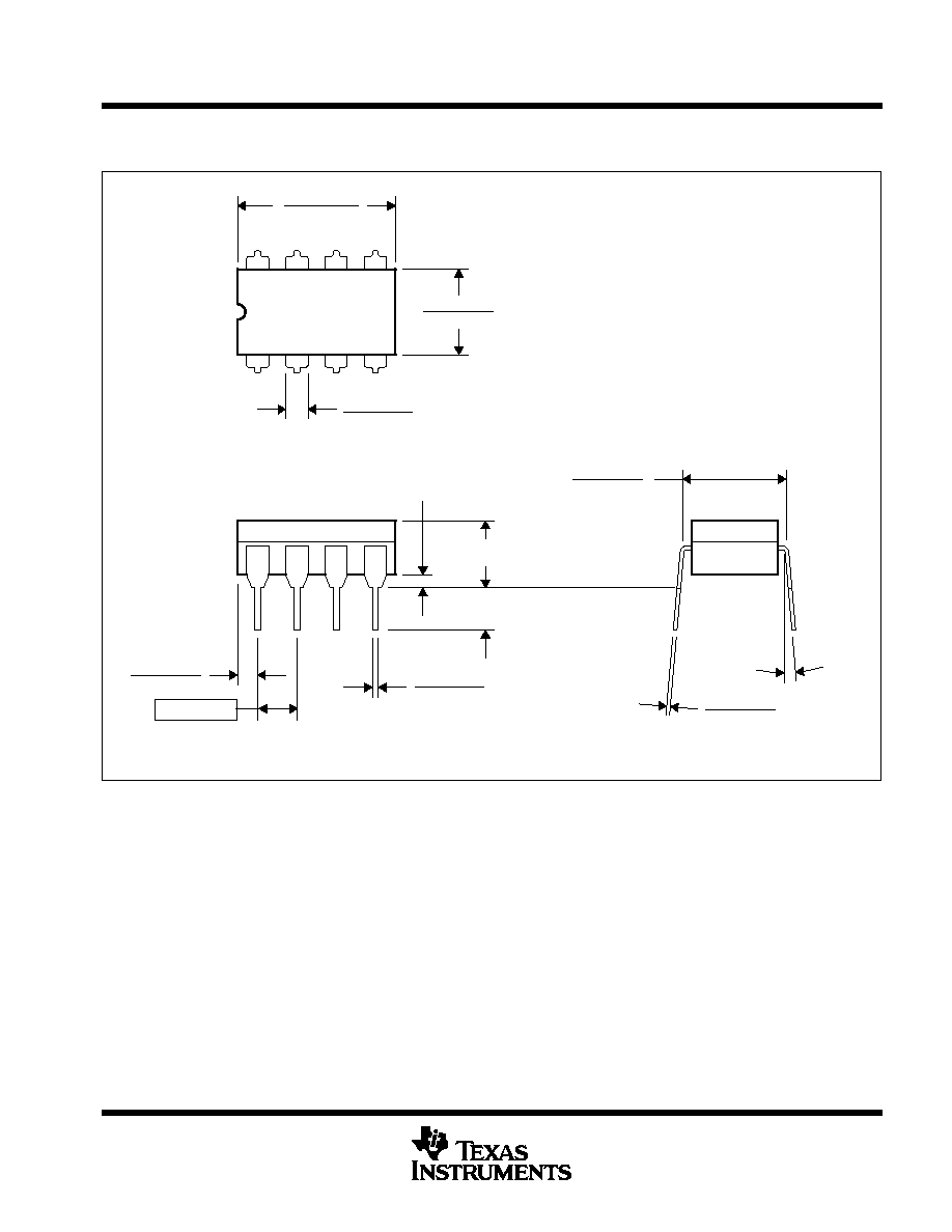
TLC220x, TLC220xA, TLC220xB, TLC220xY
Advanced LinCMOS
TM
LOW-NOISE PRECISION
OPERATIONAL AMPLIFIERS
SLOS175 ≠ FEBRUARY 1997
57
POST OFFICE BOX 655303
∑
DALLAS, TEXAS 75265
MECHANICAL INFORMATION
JG (R-GDIP-T8)
CERAMIC DUAL-IN-LINE PACKAGE
4040107 / B 04/95
0.020 (0,51) MIN
0.200 (5,08) MAX
0.130 (3,30) MIN
1
4
5
8
0
∞
≠15
∞
0.008 (0,20)
0.310 (7,87)
0.290 (7,37)
0.245 (6,22)
0.280 (7,11)
Seating Plane
0.015 (0,38)
0.015 (0,38)
0.023 (0,58)
0.400 (10,20)
0.355 (9,00)
0.063 (1,60)
0.015 (0,38)
0.065 (1,65)
0.045 (1,14)
0.100 (2,54)
NOTES: A. All linear dimensions are in inches (millimeters).
B. This drawing is subject to change without notice.
C. This package can be hermetically sealed with a ceramic lid using glass frit.
D. Index point is provided on cap for terminal identification only on press ceramic glass frit seal only
E. Falls within MIL-STD-1835 GDIP1-T8
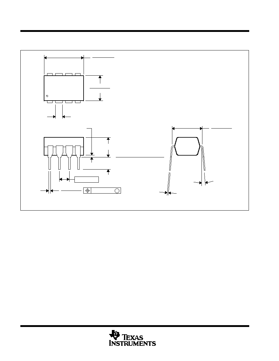
TLC220x, TLC220xA, TLC220xB, TLC220xY
Advanced LinCMOS
TM
LOW-NOISE PRECISION
OPERATIONAL AMPLIFIERS
SLOS175 ≠ FEBRUARY 1997
58
POST OFFICE BOX 655303
∑
DALLAS, TEXAS 75265
MECHANICAL INFORMATION
P (R-PDIP-T8)
PLASTIC DUAL-IN-LINE PACKAGE
4040082 / B 03/95
0.310 (7,87)
0.290 (7,37)
0.010 (0,25) NOM
0.400 (10,60)
0.355 (9,02)
5
8
4
1
0.020 (0,51) MIN
0.070 (1,78) MAX
0.240 (6,10)
0.260 (6,60)
0.200 (5,08) MAX
0.125 (3,18) MIN
0.015 (0,38)
0.021 (0,53)
Seating Plane
M
0.010 (0,25)
0.100 (2,54)
0
∞
≠ 15
∞
NOTES: A. All linear dimensions are in inches (millimeters).
B. This drawing is subject to change without notice.
C. Falls within JEDEC MS-001

IMPORTANT NOTICE
Texas Instruments and its subsidiaries (TI) reserve the right to make changes to their products or to discontinue
any product or service without notice, and advise customers to obtain the latest version of relevant information
to verify, before placing orders, that information being relied on is current and complete. All products are sold
subject to the terms and conditions of sale supplied at the time of order acknowledgment, including those
pertaining to warranty, patent infringement, and limitation of liability.
TI warrants performance of its semiconductor products to the specifications applicable at the time of sale in
accordance with TI's standard warranty. Testing and other quality control techniques are utilized to the extent
TI deems necessary to support this warranty. Specific testing of all parameters of each device is not necessarily
performed, except those mandated by government requirements.
Customers are responsible for their applications using TI components.
In order to minimize risks associated with the customer's applications, adequate design and operating
safeguards must be provided by the customer to minimize inherent or procedural hazards.
TI assumes no liability for applications assistance or customer product design. TI does not warrant or represent
that any license, either express or implied, is granted under any patent right, copyright, mask work right, or other
intellectual property right of TI covering or relating to any combination, machine, or process in which such
semiconductor products or services might be or are used. TI's publication of information regarding any third
party's products or services does not constitute TI's approval, warranty or endorsement thereof.
Copyright
©
2000, Texas Instruments Incorporated