
CY54FCT646T, CY74FCT646T
8-BIT REGISTERED TRANSCEIVERS
WITH 3-STATE OUTPUTS
SCCS031A ≠ JULY 1994 ≠ REVISED OCTOBER 2001
1
POST OFFICE BOX 655303
∑
DALLAS, TEXAS 75265
D
Function, Pinout, and Drive Compatible
With FCT and F Logic
D
Reduced V
OH
(Typically = 3.3 V) Versions
of Equivalent FCT Functions
D
Edge-Rate Control Circuitry for
Significantly Improved Noise
Characteristics
D
I
off
Supports Partial-Power-Down Mode
Operation
D
Matched Rise and Fall Times
D
Fully Compatible With TTL Input and
Output Logic Levels
D
ESD Protection Exceeds JESD 22
≠ 2000-V Human-Body Model (A114-A)
≠ 200-V Machine Model (A115-A)
≠ 1000-V Charged-Device Model (C101)
D
Independent Register for A and B Buses
D
CY54FCT646T
≠ 48-mA Output Sink Current
≠ 12-mA Output Source Current
D
CY74FCT646T
≠ 64-mA Output Sink Current
≠ 32-mA Output Source Current
D
3-State Outputs
description
The 'FCT646T devices consist of a bus
transceiver circuit with 3-state, D-type flip-flops,
and control circuitry arranged for multiplexed
transmission of data directly from the input bus or
from the internal registers. Data on the A or B bus
is clocked into the registers as the appropriate
clock pin goes to a high logic level. Output-enable (G) and direction (DIR) inputs control the transceiver function.
In the transceiver mode,data present at the high-impedance port can be stored in either the A or B register, or
in both. Select controls (SAB, SBA) can multiplex stored and real-time (transparent mode) data. DIR determines
which bus receives data when G is low. In the isolation mode (G is high), A data can be stored in the B register
and/or B data can be stored in the A register.
These devices are fully specified for partial-power-down applications using I
off
. The I
off
circuitry disables the
outputs, preventing damaging current backflow through the device when it is powered down.
Copyright
2001, Texas Instruments Incorporated
PRODUCTION DATA information is current as of publication date.
Products conform to specifications per the terms of Texas Instruments
standard warranty. Production processing does not necessarily include
testing of all parameters.
Please be aware that an important notice concerning availability, standard warranty, and use in critical applications of
Texas Instruments semiconductor products and disclaimers thereto appears at the end of this data sheet.
1
2
3
4
5
6
7
8
9
10
11
12
24
23
22
21
20
19
18
17
16
15
14
13
CPAB
SAB
DIR
A
1
A
2
A
3
A
4
A
5
A
6
A
7
A
8
GND
V
CC
CPBA
SBA
G
B
1
B
2
B
3
B
4
B
5
B
6
B
7
B
8
3
2 1 28 27
12 13
5
6
7
8
9
10
11
25
24
23
22
21
20
19
G
B
1
B
2
NC
B
3
B
4
B
5
A
1
A
2
A3
NC
A
4
A
5
A
6
4
26
14 15 16 17 18
GND
NC
B
DIR
SAB
CP
AB
NC
CPBA
SBA
V
CC
NC ≠ No internal connection
6
B
7
B
8
A
8
A
7
CY54FCT646T . . . D PACKAGE
CY74FCT646T . . . Q OR SO PACKAGE
(TOP VIEW)
CY54FCT646T . . . L PACKAGE
(TOP VIEW)
On products compliant to MIL-PRF-38535, all parameters are tested
unless otherwise noted. On all other products, production
processing does not necessarily include testing of all parameters.

CY54FCT646T, CY74FCT646T
8-BIT REGISTERED TRANSCEIVERS
WITH 3-STATE OUTPUTS
SCCS031A ≠ JULY 1994 ≠ REVISED OCTOBER 2001
2
POST OFFICE BOX 655303
∑
DALLAS, TEXAS 75265
PIN DESCRIPTION
NAME
DESCRIPTION
A
Data register A inputs, data register B outputs
B
Data register B inputs, data register A outputs
CPAB, CPBA
Clock-pulse inputs
SAB, SBA
Output data-source-select inputs
DIR, G
Output-enable inputs
ORDERING INFORMATION
TA
PACKAGE
SPEED
(ns)
ORDERABLE
PART NUMBER
TOP-SIDE
MARKING
QSOP ≠ Q
Tape and reel
5.4
CY74FCT646CTQCT
FCT646C
SOIC
SO
Tube
5.4
CY74FCT646CTSOC
FCT646C
SOIC ≠ SO
Tape and reel
5.4
CY74FCT646CTSOCT
FCT646C
QSOP ≠ Q
Tape and reel
6.3
CY74FCT646ATQCT
FCT646A
≠40
∞
C to 85
∞
C
SOIC
SO
Tube
6.3
CY74FCT646ATSOC
FCT646A
SOIC ≠ SO
Tape and reel
6.3
CY74FCT646ATSOCT
FCT646A
QSOP ≠ Q
Tape and reel
9
CY74FCT646TQCT
FCT646
SOIC
SO
Tube
9
CY74FCT646TSOC
FCT646
SOIC ≠ SO
Tape and reel
9
CY74FCT646TSOCT
FCT646
LCC ≠ L
Tube
6
CY54FCT646CTLMB
55
∞
C to 125
∞
C
CDIP ≠ D
Tube
7.7
CY54FCT646ATDMB
≠55
∞
C to 125
∞
C
LCC
L
Tube
7.7
CY54FCT646ATLMB
LCC ≠ L
Tube
11
CY54FCT646TLMB
Package drawings, standard packing quantities, thermal data, symbolization, and PCB design guidelines are
available at www.ti.com/sc/package.
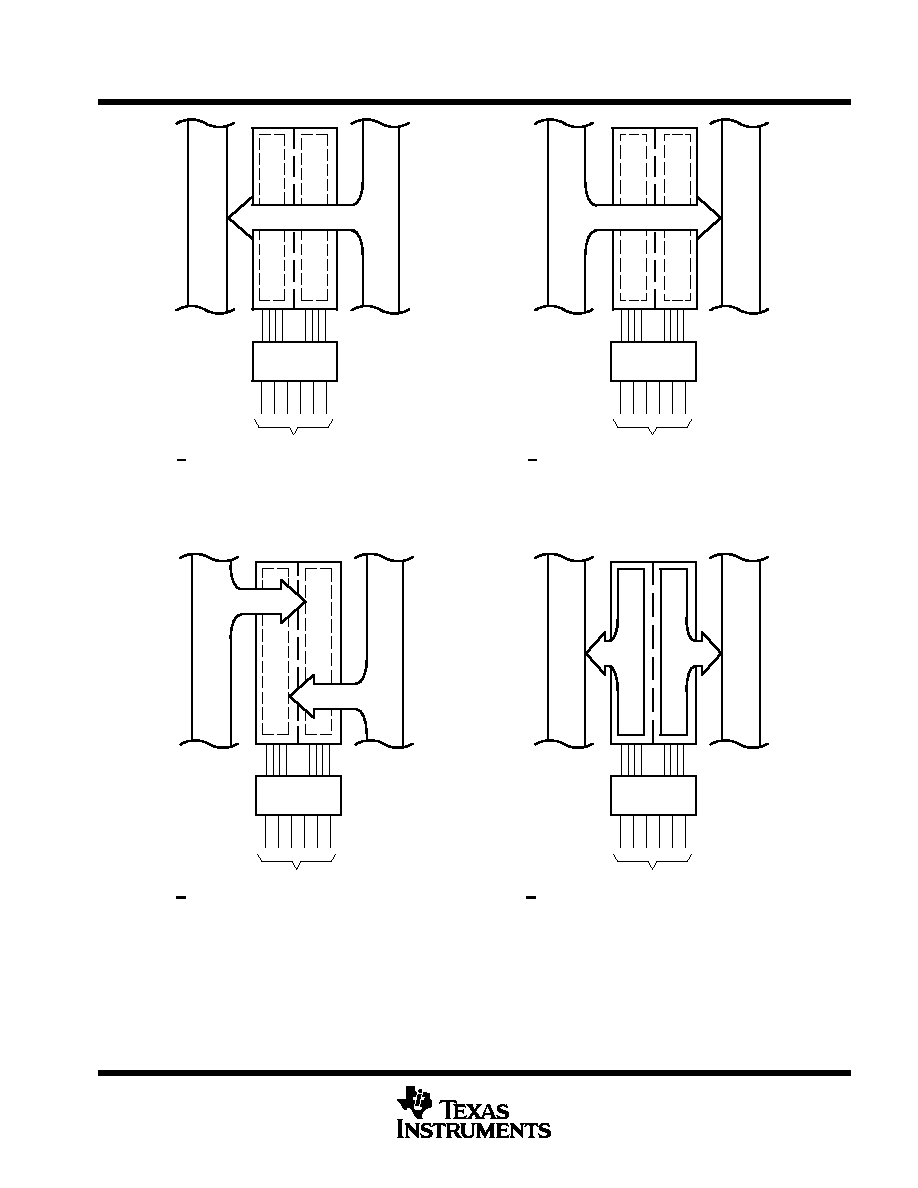
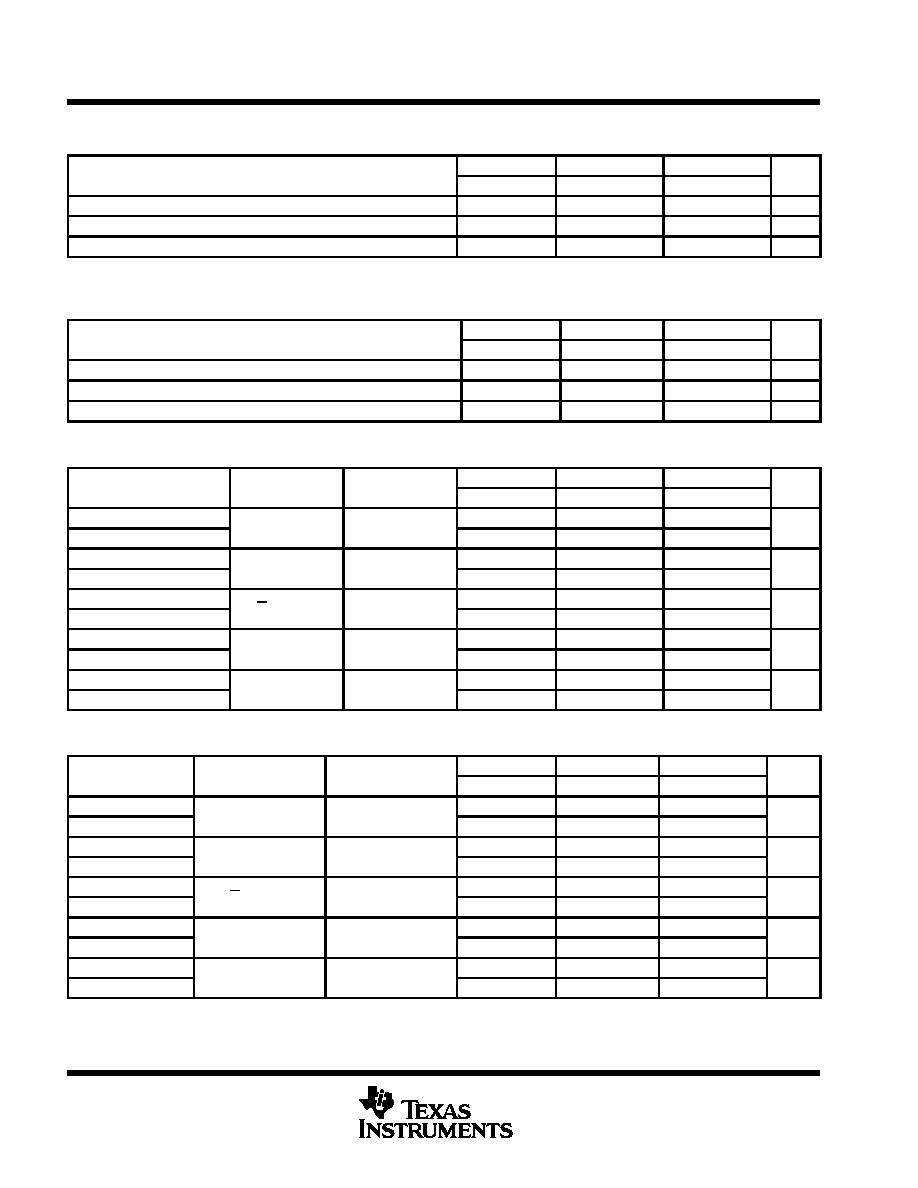
FUNCTION TABLE
INPUTS
DATA I/O
OPERATION
G
DIR
CPAB
CPBA
SAB
SBA
A1≠A8
B1≠B8
OR FUNCTION
H
X
H or L
H or L
X
X
Input
Input
Isolation
H
X
X
X
Input
Input
Store A and B data
L
L
X
X
X
L
Output
Input
Real-time B data to A bus
L
L
X
H or L
X
H
Output
Input
Stored B data to A bus
L
H
X
X
L
X
Input
Output
Real-time A data to B bus
L
H
H or L
X
H
X
Input
Output
Stored A data to B bus
H = High logic level, L = Low logic level,
= Low-to-high transition, X = Don't care
The data output functions can be enabled or disabled by various signals at the G or DIR inputs. Data input
functions always are enabled, i.e., data at the bus pins is stored on every low-to-high transition of the
clock inputs.
CY54FCT646T, CY74FCT646T
8-BIT REGISTERED TRANSCEIVERS
WITH 3-STATE OUTPUTS
SCCS031A ≠ JULY 1994 ≠ REVISED OCTOBER 2001
3
POST OFFICE BOX 655303
∑
DALLAS, TEXAS 75265
21
L
3
DIR
L
1
CPAB
X
23
CPBA
X
2
SAB
X
22
SBA
L
21
L
3
DIR
H
1
CPAB
X
23
CPBA
X
2
SAB
L
22
SBA
X
21
L
3
DIR
H
1
CPAB
23
CPBA
X
2
SAB
X
22
SBA
X
21
L
3
L
1
CPAB
X
23
CPBA
H or L
2
SAB
X
22
SBA
H
L
H
L
X
X
X
X
X
X
L
H
H or L
X
H
X
BUS B
BUS A
BUS B
BUS A
BUS B
BUS A
BUS B
BUS A
G
G
G
REAL-TIME TRANSFER
BUS B TO BUS A
REAL-TIME TRANSFER
BUS A TO BUS B
STORAGE FROM
A AND/OR B
TRANSFER STORED DATA
TO A AND/OR B
DIR
Cannot transfer data to A bus and B bus simultaneously.
G
Figure 1. Bus-Management Functions
CY54FCT646T, CY74FCT646T
8-BIT REGISTERED TRANSCEIVERS
WITH 3-STATE OUTPUTS
SCCS031A ≠ JULY 1994 ≠ REVISED OCTOBER 2001
4
POST OFFICE BOX 655303
∑
DALLAS, TEXAS 75265
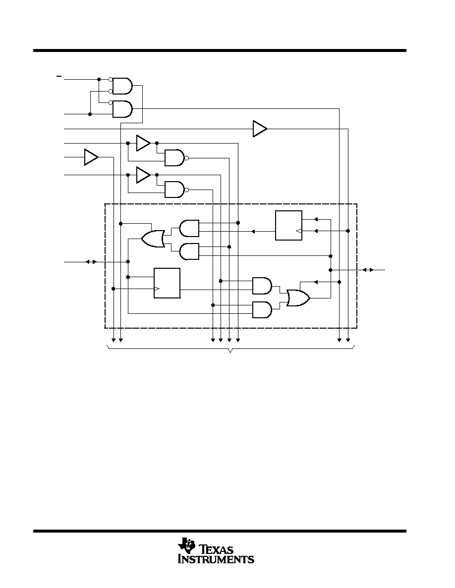
logic diagram (positive logic)
A1
B1
One of Eight Channels
SAB
CPAB
SBA
CPBA
DIR
G
To Seven Other Channels
21
3
23
22
1
2
4
20
D
C
D
C
Pin numbers shown are for the Q and SO packages.
absolute maximum ratings over operating free-air temperature range (unless otherwise noted)
Supply voltage range to ground potential
≠0.5 V to 7 V
. . . . . . . . . . . . . . . . . . . . . . . . . . . . . . . . . . . . . . . . . . . . . .
DC input voltage range
≠0.5 V to 7 V
. . . . . . . . . . . . . . . . . . . . . . . . . . . . . . . . . . . . . . . . . . . . . . . . . . . . . . . . . . . . .
DC output voltage range
≠0.5 V to 7 V
. . . . . . . . . . . . . . . . . . . . . . . . . . . . . . . . . . . . . . . . . . . . . . . . . . . . . . . . . . . .
DC output current (maximum sink current/pin)
120 mA
. . . . . . . . . . . . . . . . . . . . . . . . . . . . . . . . . . . . . . . . . . . . . .
Package thermal impedance,
JA
(see Note 1): Q package
61
∞
C/W
. . . . . . . . . . . . . . . . . . . . . . . . . . . . . . . . . .
SO package
46
∞
C/W
. . . . . . . . . . . . . . . . . . . . . . . . . . . . . . . . .
Ambient temperature range with power applied, T
A
≠65
∞
C to 135
∞
C
. . . . . . . . . . . . . . . . . . . . . . . . . . . . . . . . . . .
Storage temperature range, T
stg
≠65
∞
C to 150
∞
C
. . . . . . . . . . . . . . . . . . . . . . . . . . . . . . . . . . . . . . . . . . . . . . . . . . .
Stresses beyond those listed under "absolute maximum ratings" may cause permanent damage to the device. These are stress ratings only, and
functional operation of the device at these or any other conditions beyond those indicated under "recommended operating conditions" is not implied.
Exposure to absolute-maximum-rated conditions for extended periods may affect device reliability.
NOTE 1: The package thermal impedance is calculated in accordance with JESD 51-7.
CY54FCT646T, CY74FCT646T
8-BIT REGISTERED TRANSCEIVERS
WITH 3-STATE OUTPUTS
SCCS031A ≠ JULY 1994 ≠ REVISED OCTOBER 2001
5
POST OFFICE BOX 655303
∑
DALLAS, TEXAS 75265
recommended operating conditions (see Note 2)
CY54FCT646T
CY74FCT646T
UNIT
MIN
NOM
MAX
MIN
NOM
MAX
UNIT
VCC
Supply voltage
4.5
5
5.5
4.75
5
5.25
V
VIH
High-level input voltage
2
2
V
VIL
Low-level input voltage
0.8
0.8
V
IOH
High-level output current
≠12
≠32
mA
IOL
Low-level output current
48
64
mA
TA
Operating free-air temperature
≠55
125
≠40
85
∞
C
NOTE 2: All unused inputs of the device must be held at VCC or GND to ensure proper device operation.

CY54FCT646T, CY74FCT646T
8-BIT REGISTERED TRANSCEIVERS
WITH 3-STATE OUTPUTS
SCCS031A ≠ JULY 1994 ≠ REVISED OCTOBER 2001
6
POST OFFICE BOX 655303
∑
DALLAS, TEXAS 75265
electrical characteristics over recommended operating free-air temperature range (unless
otherwise noted)
PARAMETER
TEST CONDITIONS
CY54FCT646T
CY74FCT646T
UNIT
PARAMETER
TEST CONDITIONS
MIN
TYP
MAX
MIN
TYP
MAX
UNIT
VIK
VCC = 4.5 V,
IIN = ≠18 mA
≠0.7
≠1.2
V
VIK
VCC = 4.75 V,
IIN = ≠18 mA
≠0.7
≠1.2
V
VCC = 4.5 V,
IOH = ≠12 mA
2.4
3.3
VOH
VCC 4 75 V
IOH = ≠32 mA
2
V
VCC = 4.75 V
IOH = ≠15 mA
2.4
3.3
VOL
VCC = 4.5 V,
IOL = 48 mA
0.3
0.55
V
VOL
VCC = 4.75 V,
IOL = 64 mA
0.3
0.55
V
Vhys
All inputs
0.2
0.2
V
II
VCC = 5.5 V,
VIN = VCC
5
µ
A
II
VCC = 5.25 V,
VIN = VCC
5
µ
A
IIH
VCC = 5.5 V,
VIN = 2.7 V
±
1
µ
A
IIH
VCC = 5.25 V,
VIN = 2.7 V
±
1
µ
A
IIL
VCC = 5.5 V,
VIN = 0.5 V
±
1
µ
A
IIL
VCC = 5.25 V,
VIN = 0.5 V
±
1
µ
A
IOZH
VCC = 5.5 V,
VOUT = 2.7 V
10
µ
A
IOZH
VCC = 5.25 V,
VOUT = 2.7 V
10
µ
A
IOZL
VCC = 5.5 V,
VOUT = 0.5 V
≠10
µ
A
IOZL
VCC = 5.25 V,
VOUT = 0.5 V
≠10
µ
A
IOS
VCC = 5.5 V,
VOUT = 0 V
≠60
≠120
≠225
mA
IOS
VCC = 5.25 V,
VOUT = 0 V
≠60
≠120
≠225
mA
Ioff
VCC = 0 V,
VOUT = 4.5 V
±
1
±
1
µ
A
ICC
VCC = 5.5 V,
VIN
0.2 V,
VIN
VCC ≠ 0.2 V
0.1
0.2
mA
ICC
VCC = 5.25 V,
VIN
0.2 V,
VIN
VCC ≠ 0.2 V
0.1
0.2
mA
ICC
VCC = 5.5 V, VIN = 3.4 Vß, f1 = 0, Outputs open
0.5
2
mA
ICC
VCC = 5.25 V, VIN = 3.4 Vß, f1 = 0, Outputs open
0.5
2
mA
ICCD∂
VCC = 5.5 V, One input switching at 50% duty cycle,
Outputs open, G = DIR = GND, SAB = SBA = GND,
VIN
0.2 V or VIN
VCC ≠ 0.2 V
0.06
0.12
mA/
ICCD∂
VCC = 5.25 V, One input switching at 50% duty cycle,
Outputs open, G = DIR = GND, SAB = SBA = GND,
VIN
0.2 V or VIN
VCC ≠ 0.2 V
0.06
0.12
MHz
Typical values are at VCC = 5 V, TA = 25
∞
C.
Not more than one output should be shorted at a time. Duration of short should not exceed one second. The use of high-speed test apparatus and/or
sample-and-hold techniques are preferable to minimize internal chip heating and more accurately reflect operational values. Otherwise, prolonged
shorting of a high output can raise the chip temperature well above normal and cause invalid readings in other parametric tests. In any sequence
of parameter tests, IOS tests should be performed last.
ß Per TTL-driven input (VIN = 3.4 V); all other inputs at VCC or GND
∂ This parameter is derived for use in total power-supply calculations.
CY54FCT646T, CY74FCT646T
8-BIT REGISTERED TRANSCEIVERS
WITH 3-STATE OUTPUTS
SCCS031A ≠ JULY 1994 ≠ REVISED OCTOBER 2001
7
POST OFFICE BOX 655303
∑
DALLAS, TEXAS 75265
electrical characteristics over recommended operating free-air temperature range (unless
otherwise noted) (continued)
PARAMETER
TEST CONDITIONS
CY54FCT646T
CY74FCT646T
UNIT
PARAMETER
TEST CONDITIONS
MIN
TYP
MAX
MIN
TYP
MAX
UNIT
#
V
5 5 V
One bit
switching
at f1 = 5 MHz
VIN
0.2 V or
VIN
VCC ≠ 0.2 V
0.7
1.4
#
VCC = 5.5 V,
f0 = 10 MHz,
Outputs open
1
at 50% duty
cycle
VIN = 3.4 V or GND
1.2
3.4
mA
#
Outputs open,
G = DIR = GND,
SAB = SBA = GND
Eight bits
switching
at f1 = 5 MHz
VIN
0.2 V or
VIN
VCC ≠ 0.2 V
2.8
5.6||
mA
IC#
1
at 50% duty
cycle
VIN = 3.4 V or GND
5.1
14.6||
IC#
V
5 25 V
One bit
switching
at f1 = 5 MHz
VIN
0.2 V or
VIN
VCC ≠ 0.2 V
0.7
1.4
VCC = 5.25 V,
f0 = 10 MHz,
Outputs open
1
at 50% duty
cycle
VIN = 3.4 V or GND
1.2
3.4
mA
Outputs open,
G = DIR = GND,
SAB = SBA = GND
Eight bits
switching
at f1 = 5 MHz
VIN
0.2 V or
VIN
VCC ≠ 0.2 V
2.8
5.6||
mA
1
at 50% duty
cycle
VIN = 3.4 V or GND
5.1
14.6||
Ci
6
10
6
10
pF
Co
8
12
8
12
pF
# IC
= ICC +
ICC
◊
DH
◊
NT + ICCD(f0/2 + f1
◊
N1)
Where:
IC
= Total supply current
ICC
= Power-supply current with CMOS input levels
ICC = Power-supply current for a TTL high input (VIN = 3.4 V)
DH
= Duty cycle for TTL inputs high
NT
= Number of TTL inputs at DH
ICCD = Dynamic current caused by an input transition pair (HLH or LHL)
f0
= Clock frequency for registered devices, otherwise zero
f1
= Input signal frequency
N1
= Number of inputs changing at f1
All currents are in milliamperes and all frequencies are in megahertz.
|| Values for these conditions are examples of the ICC formula.
CY54FCT646T, CY74FCT646T
8-BIT REGISTERED TRANSCEIVERS
WITH 3-STATE OUTPUTS
SCCS031A ≠ JULY 1994 ≠ REVISED OCTOBER 2001
8
POST OFFICE BOX 655303
∑
DALLAS, TEXAS 75265
timing requirements over recommended operating free-air temperature range (unless otherwise
noted) (see Figure 2)
CY54FCT646T
CY54FCT646AT
CY54FCT646CT
UNIT
MIN
MAX
MIN
MAX
MIN
MAX
UNIT
tw
Pulse duration
6
5
5
ns
tsu
Setup time, data before CPAB
or CPBA
4.5
2
2
ns
th
Hold time, data after CPAB
or CPBA
2
1.5
1.5
ns
timing requirements over recommended operating free-air temperature range (unless otherwise
noted) (see Figure 2)
CY74FCT646T
CY74FCT646AT
CY74FCT646CT
UNIT
MIN
MAX
MIN
MAX
MIN
MAX
UNIT
tw
Pulse duration
6
5
5
ns
tsu
Setup time, data before CPAB
or CPBA
4
2
2
ns
th
Hold time, data after CPAB
or CPBA
2
1.5
1.5
ns
switching characteristics over operating free-air temperature range (see Figure 2)
PARAMETER
FROM
TO
CY54FCT646T
CY54FCT646AT
CY54FCT646CT
UNIT
PARAMETER
(INPUT)
(OUTPUT)
MIN
MAX
MIN
MAX
MIN
MAX
UNIT
tPLH
A or B
B or A
2
11
2
7.7
1.5
6
ns
tPHL
A or B
B or A
2
11
2
7.7
1.5
6
ns
tPZH
DIR
A or B
2
15
2
10.5
1.5
8.9
ns
tPZL
DIR
A or B
2
15
2
10.5
1.5
8.9
ns
tPHZ
G and DIR
A or B
2
11
2
7.7
1.5
7.7
ns
tPLZ
G and DIR
A or B
2
11
2
7.7
1.5
7.7
ns
tPLH
CPAB or CPBA
A or B
2
10
2
7
1.5
6.3
ns
tPHL
CPAB or CPBA
A or B
2
10
2
7
1.5
6.3
ns
tPLH
SBA or SAB
A or B
2
12
2
8.4
1.5
7
ns
tPHL
SBA or SAB
A or B
2
12
2
8.4
1.5
7
ns
switching characteristics over operating free-air temperature range (see Figure 2)
PARAMETER
FROM
TO
CY74FCT646T
CY74FCT646AT
CY74FCT646CT
UNIT
PARAMETER
(INPUT)
(OUTPUT)
MIN
MAX
MIN
MAX
MIN
MAX
UNIT
tPLH
A or B
B or A
1.5
9
1.5
6.3
1.5
5.4
ns
tPHL
A or B
B or A
1.5
9
1.5
6.3
1.5
5.4
ns
tPZH
DIR
A or B
1.5
14
1.5
9.8
1.5
7.8
ns
tPZL
DIR
A or B
1.5
14
1.5
9.8
1.5
7.8
ns
tPHZ
G and DIR
A or B
1.5
9
1.5
6.3
1.5
6.3
ns
tPLZ
G and DIR
A or B
1.5
9
1.5
6.3
1.5
6.3
ns
tPLH
CPAB or CPBA
A or B
1.5
9
1.5
6.3
1.5
5.7
ns
tPHL
CPAB or CPBA
A or B
1.5
9
1.5
6.3
1.5
5.7
ns
tPLH
SBA or SAB
A or B
1.5
11
1.5
7.7
1.5
6.2
ns
tPHL
SBA or SAB
A or B
1.5
11
1.5
7.7
1.5
6.2
ns
CY54FCT646T, CY74FCT646T
8-BIT REGISTERED TRANSCEIVERS
WITH 3-STATE OUTPUTS
SCCS031A ≠ JULY 1994 ≠ REVISED OCTOBER 2001
9
POST OFFICE BOX 655303
∑
DALLAS, TEXAS 75265
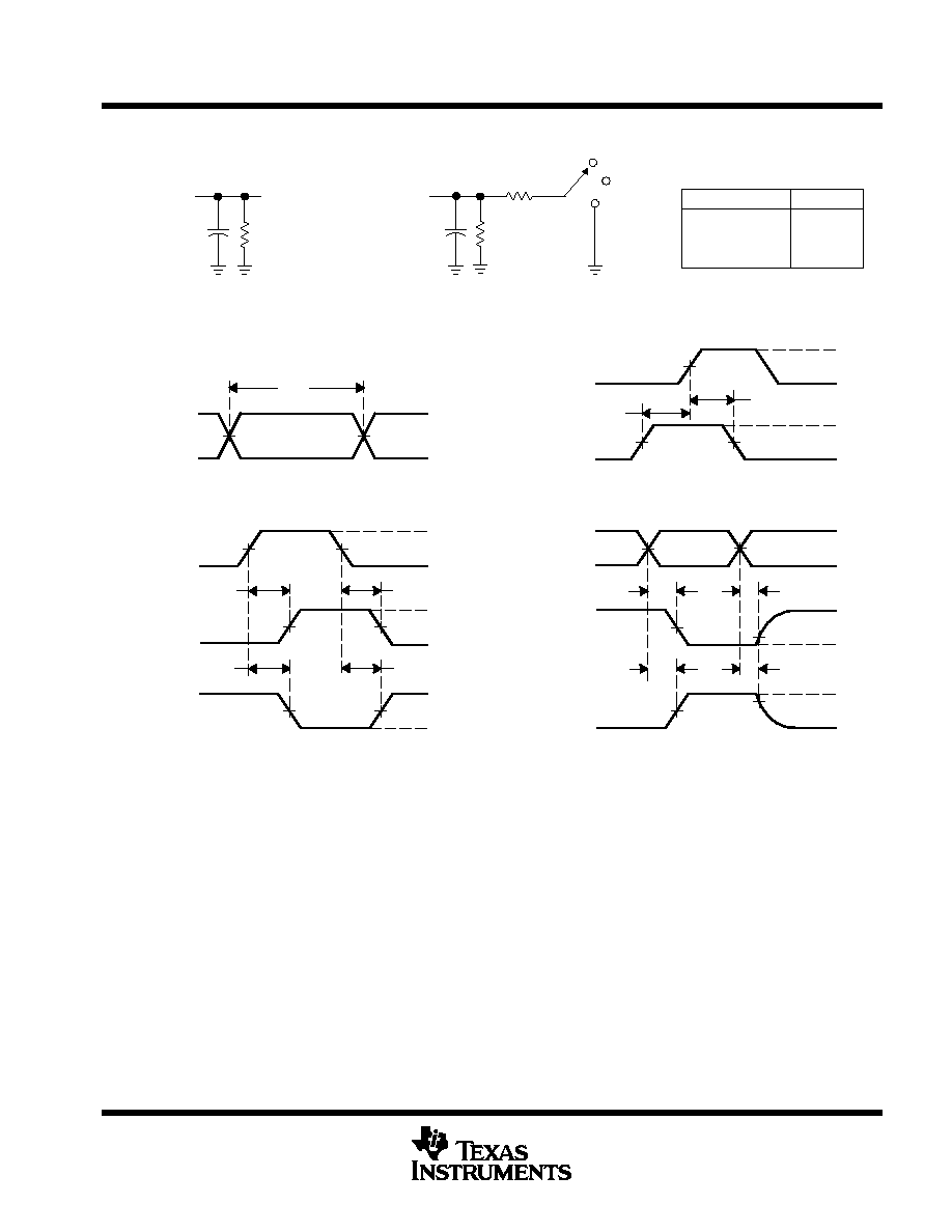
PARAMETER MEASUREMENT INFORMATION
3 V
3 V
0 V
0 V
th
tsu
VOLTAGE WAVEFORMS
SETUP AND HOLD TIMES
Data Input
tPLH
tPHL
tPHL
tPLH
VOH
VOH
VOL
VOL
3 V
0 V
Input
Out-of-Phase
Output
In-Phase
Output
Timing Input
VOLTAGE WAVEFORMS
PROPAGATION DELAY TIMES
INVERTING AND NONINVERTING OUTPUTS
Output
Control
Output
Waveform 1
(see Note B)
Output
Waveform 2
(see Note B)
VOL
VOH
tPZL
tPZH
tPLZ
tPHZ
3.5 V
0 V
VOL
+ 0.3 V
0 V
3 V
VOLTAGE WAVEFORMS
ENABLE AND DISABLE TIMES
LOW- AND HIGH-LEVEL ENABLING
tPLH/tPHL
tPLZ/tPZL
tPHZ/tPZH
Open
7 V
Open
TEST
S1
3 V
0 V
tw
VOLTAGE WAVEFORMS
PULSE DURATION
Input
NOTES: A. CL includes probe and jig capacitance.
B. Waveform 1 is for an output with internal conditions such that the output is low except when disabled by the output control.
Waveform 2 is for an output with internal conditions such that the output is high except when disabled by the output control.
C. The outputs are measured one at a time with one input transition per measurement.
From Output
Under Test
CL = 50 pF
(see Note A)
LOAD CIRCUIT FOR
3-STATE OUTPUTS
S1
7 V
500
GND
From Output
Under Test
CL = 50 pF
(see Note A)
Test
Point
LOAD CIRCUIT FOR
TOTEM-POLE OUTPUTS
Open
VOH ≠
0.3 V
500
500
1.5 V
1.5 V
1.5 V
1.5 V
1.5 V
1.5 V
1.5 V
1.5 V
1.5 V
1.5 V
1.5 V
1.5 V
1.5 V
1.5 V
1.5 V
Figure 2. Load Circuit and Voltage Waveforms

IMPORTANT NOTICE
Texas Instruments Incorporated and its subsidiaries (TI) reserve the right to make corrections, modifications,
enhancements, improvements, and other changes to its products and services at any time and to discontinue
any product or service without notice. Customers should obtain the latest relevant information before placing
orders and should verify that such information is current and complete. All products are sold subject to TI's terms
and conditions of sale supplied at the time of order acknowledgment.
TI warrants performance of its hardware products to the specifications applicable at the time of sale in
accordance with TI's standard warranty. Testing and other quality control techniques are used to the extent TI
deems necessary to support this warranty. Except where mandated by government requirements, testing of all
parameters of each product is not necessarily performed.
TI assumes no liability for applications assistance or customer product design. Customers are responsible for
their products and applications using TI components. To minimize the risks associated with customer products
and applications, customers should provide adequate design and operating safeguards.
TI does not warrant or represent that any license, either express or implied, is granted under any TI patent right,
copyright, mask work right, or other TI intellectual property right relating to any combination, machine, or process
in which TI products or services are used. Information published by TI regarding third≠party products or services
does not constitute a license from TI to use such products or services or a warranty or endorsement thereof.
Use of such information may require a license from a third party under the patents or other intellectual property
of the third party, or a license from TI under the patents or other intellectual property of TI.
Reproduction of information in TI data books or data sheets is permissible only if reproduction is without
alteration and is accompanied by all associated warranties, conditions, limitations, and notices. Reproduction
of this information with alteration is an unfair and deceptive business practice. TI is not responsible or liable for
such altered documentation.
Resale of TI products or services with statements different from or beyond the parameters stated by TI for that
product or service voids all express and any implied warranties for the associated TI product or service and
is an unfair and deceptive business practice. TI is not responsible or liable for any such statements.
Mailing Address:
Texas Instruments
Post Office Box 655303
Dallas, Texas 75265
Copyright
2001, Texas Instruments Incorporated