
SMJ320C50/SMQ320C50
DIGITAL SIGNAL PROCESSOR
SGUS020B ≠ JUNE 1996 ≠ REVISED SEPTEMBER 2001
1
POST OFFICE BOX 1443
∑
HOUSTON, TEXAS 77251≠1443
D
Military Operating Temperature Range:
≠ 55
∞
C to 125
∞
C
D
Processed to MIL-PRF-38535
D
Fast Instruction Cycle Time (30 ns and
40 ns)
D
Source-Code Compatible With All C1x
and C2x Devices
D
RAM-Based Operation
≠ 9K
◊
16-Bit Single-Cycle On-Chip
Program/Data RAM
≠ 1056
◊
16-Bit Dual-Access On-Chip
Data RAM
D
2K
◊
16-Bit On-Chip Boot ROM
D
224K
◊
16-Bit Maximum Addressable
External Memory Space (64K Program,
64K Data, 64K I/O, and 32K Global)
D
32-Bit Arithmetic Logic Unit (ALU)
≠ 32-bit Accumulator (ACC)
≠ 32-Bit Accumulator Buffer (ACCB)
D
16-Bit Parallel Logic Unit (PLU)
D
16
◊
16-Bit Multiplier, 32-Bit Product
D
11 Context-Switch Registers
D
Two Buffers for Circular Addressing
D
Full-Duplex Synchronous Serial Port
D
Time-Division Multiplexed Serial Port (TDM)
D
Timer With Control and Counter Registers
D
16 Software Programmable Wait-State
Generators
D
Divide-by-One Clock Option
D
IEEE 1149.1
Boundary Scan Logic
D
Operations Are Fully Static
D
Enhanced Performance Implanted CMOS
(EPIC
) Technology Fabricated by Texas
Instruments
D
Packaging
≠ 141-Pin Ceramic Grid Array (GFA Suffix)
≠ 132-Lead Ceramic Quad Flat Package
(HFG Suffix)
≠ 132-Lead Plastic Quad Flat Package
(PQ Suffix)
Please be aware that an important notice concerning availability, standard warranty, and use in critical applications of
Texas Instruments semiconductor products and disclaimers thereto appears at the end of this data sheet.
HFG PACKAGE
(TOP VIEW)
……
……
……
……
……
……
……
……
……
……
……
……
……
……
……
……
100
99
1
132
66
34
67
33
2
1 3 5 7 9 11 13 15 17 19
V
T
P
M
K
H
F
D
B
W
U
R
N
L
J
G
E
C
A
4
6
8 10 12 14 16 18
GFA PACKAGE
(TOP VIEW)
PQ PACKAGE
(TOP VIEW)
1
17
18
117
116
50
51
83
84
132
PRODUCTION DATA information is current as of publication date.
Products conform to specifications per the terms of Texas Instruments
standard warranty. Production processing does not necessarily include
testing of all parameters.
Copyright
1998, Texas Instruments Incorporated
IEEE Standard 1149.1-1990 Standard-Test-Access Port and Boundary Scan Architecture
EPIC is a trademark of Texas Instruments Incorporated.
On products compliant to MIL STD 883, Class B, all parameters are
tested unless otherwise noted. On all other products, production
processing does not necessarily include testing of all parameters.
SMJ320C50/SMQ320C50
DIGITAL SIGNAL PROCESSOR
SGUS020B ≠ JUNE 1996 ≠ REVISED SEPTEMBER 2001
2
POST OFFICE BOX 1443
∑
HOUSTON, TEXAS 77251≠1443
description
The SMJ320C50 digital signal processor (DSP) is a high-performance, 16-bit, fixed-point processor
manufactured in 0.72-
µ
m double-level metal CMOS technology. The SMJ320C50 is the first DSP from TI
designed as a fully static device. Full-static CMOS design contributes to low power consumption while
maintaining high performance, making it ideal for applications such as battery-operated communications
systems, satellite systems, and advanced control algorithms.
A number of enhancements to the basic SMJ320C2x architecture give the C50 a minimum 2
◊
performance over
the previous generation. A four-deep instruction pipeline, that incorporates delayed branching, delayed call to
subroutine, and delayed return from subroutine, allows the C50 to perform instructions in fewer cycles. The
addition of a parallel logic unit (PLU) gives the C50 a method for manipulating bits in data memory without using
the accumulator and ALU. The C50 has additional shifting and scaling capability for proper alignment of
multiplicands or storage of values to data memory.
The C50 achieves its low-power consumption through the IDLE2 instruction. IDLE2 removes the functional
clock from the internal hardware of the C50, which puts it into a total-sleep mode that uses only 7
µ
A. A low-logic
level on an external interrupt with a duration of at least five clock cycles ends the IDLE2 mode.
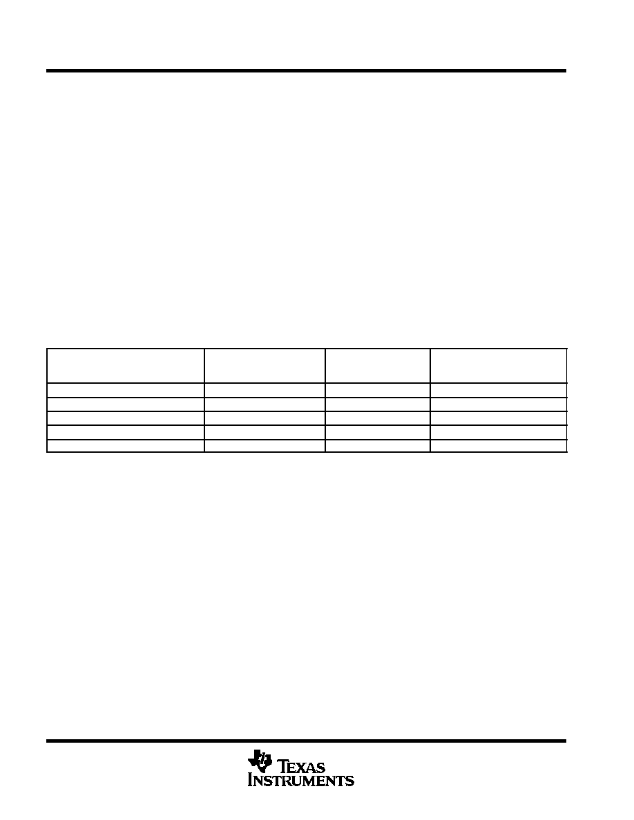
The C50 is available with two clock speeds. The clock frequencies are 50 MHz, providing a 40-ns cycle time,
and 66 MHz, providing a 30-ns cycle time. The available options are listed in Table 1.
Table 1. Available Options
PART NUMBER
SPEED
SUPPLY
VOLTAGE
TOLERANCE
PACKAGE
SMJ320C50GFAM66
30-ns cycle time
±
5%
Pin grid array
SMJ320C50HFGM66
30-ns cycle time
±
5%
Quad flat package
SMJ320C50GFAM50
40 ns cycle time
±
5%
Pin grid array
SMJ320C50HFGM50
40 ns cycle time
±
5%
Quad flat package
SMQ320C50PQM66
30 ns cycle time
±
5%
Plastic Quad flat package
When ordering, use DESC P/N 5962-9455804NZD

SMJ320C50/SMQ320C50
DIGITAL SIGNAL PROCESSOR
SGUS020B ≠ JUNE 1996 ≠ REVISED SEPTEMBER 2001
3
POST OFFICE BOX 1443
∑
HOUSTON, TEXAS 77251≠1443
functional block diagram
BMAR
MUX
PC(16)
Stack
(8
◊
16)
PASR
BRAF
IPTR
INT#
INTM
IMR
IFR
MP/MC
CNF
RAM
Program Memory
PAER
Compare
BRCR
MUX
MUX
MUX
MUX
TRM
TREG0
TREG1
TREG2
COUNT
Prescaler
OVM
SXM
Multiplier
PREG(32)
PM
P-Scaler
ALU(32)
ACC(32)
ACCB(32)
Post-Scaler
OV
TC
C
DBMR
BIM
MUX
PLU(16)
MUX
MUX
MUX
CBER
MUX
INDX
ARCR
ARP
ARB
NDX
CBSR
DP(9)
dma(7)
AUXREGS
(8
◊
16)
CBCR
XF
ARAU(16)
Data Memory
GREG
BR
CNF
OVLY
Program Bus (Address)
Program Bus (Data)
Data Bus (Address)
Data Bus (Data)
Data Bus (Data)

SMJ320C50/SMQ320C50
DIGITAL SIGNAL PROCESSOR
SGUS020B ≠ JUNE 1996 ≠ REVISED SEPTEMBER 2001
4
POST OFFICE BOX 1443
∑
HOUSTON, TEXAS 77251≠1443
terminal assignments
NAME
PQ PKG
HFG PKG
GFA PKG
NAME
PQ PKG
HFG PKG
GFA PKG
NC
18
1
A2
57
40
W3
NC
19
2
A3
58
41
U7
VSS3
20
3
D8
A4
59
42
V6
VSS4
21
4
D10
A5
60
43
W5
NC
22
5
A6
61
44
U9
D7
23
6
E3
A7
62
45
V8
D6
24
7
D2
A8
63
46
W7
D5
25
8
C1
A9
64
47
W9
D4
26
9
G3
VDD7
65
48
E9
D3
27
10
F2
VDD8
66
49
E11
D2
28
11
E1
TDI
67
50
V10
D1
29
12
J3
VSS9
68
51
K4
D0(LSB)
30
13
H2
VSS10
69
52
M4
TMS
31
14
G1
NC
70
53
VDD3
32
15
C3
CLKMD1
71
54
W11
VDD4
33
16
D4
A10
72
55
W13
TCK
34
17
J1
A11
73
56
V12
VSS5
35
18
D12
A12
74
57
U11
VSS6
36
19
F4
A13
75
58
W15
NC
37
20
A14
76
59
V14
INT1
38
21
L1
A15(MSB)
77
60
U13
INT2
39
22
N1
NC
78
61
INT3
40
23
M2
NC
79
62
INT4
41
24
L3
VDD9
80
63
E13
NMI
42
25
R1
VDD10
81
64
G5
DR
43
26
P2
RD
82
65
V16
TDR
44
27
N3
WE
83
66
U15
FSR
45
28
T2
NC
84
67
CLKR
46
29
R3
NC
85
68
VDD5
47
30
E5
VSS11
86
69
P4
VDD6
48
31
E7
VSS12
87
70
T4
NC
49
32
NC
88
71
NC
50
33
DS
89
72
R17
NC
51
34
IS
90
73
T18
NC
52
35
PS
91
74
U19
VSS7
53
36
H4
R/W
92
75
N17
VSS8
54
37
K2
STRB
93
76
P18
A0
55
38
U5
BR
94
77
R19
A1
56
39
V4
CLKIN2
95
78
L17
NC = No internal connection
GFA Package additional connections:
VDD: R11, E15, G15, J15, L15, N15, R13, R15, T16, U17, V18, W17, W19
VSS: T14, U1, U3, V2, W1, C17, C19, D14, D16, D18, F16, H16, K16, M16, P16

SMJ320C50/SMQ320C50
DIGITAL SIGNAL PROCESSOR
SGUS020B ≠ JUNE 1996 ≠ REVISED SEPTEMBER 2001
5
POST OFFICE BOX 1443
∑
HOUSTON, TEXAS 77251≠1443
terminal assignments (continued)
NAME
PQ PKG
HFG PKG
GFA PKG
NAME
PQ PKG
HFG PKG
GFA PKG
X2/CLKIN
96
79
M18
TCLKX
123
106
B16
X1
97
80
N19
CLKX
124
107
A17
VDD11
98
81
J5
TFSR/TADD
125
108
C13
VDD12
99
82
L5
TCLKR
126
109
B14
TDO
100
83
L19
RS
127
110
A15
VSS13
101
84
T6
READY
128
111
C11
VSS14
102
85
T8
HOLD
129
112
B12
CLKMD2
103
86
K18
BIO
130
113
A13
FSX
104
87
J19
VDD15
131
114
R7
TFSX/TFRM
105
88
G19
VDD16
132
115
R9
DX
106
89
H18
IAQ
1
116
A11
TDX
107
90
J17
TRST
2
117
A9
HOLDA
108
91
E19
VSS1
3
118
B10
XF
109
92
F18
VSS2
4
119
D6
CLKOUT1
110
93
G17
MP/MC
5
120
A7
NC
111
94
D15(MSB)
6
121
B8
IACK
112
95
E17
D14
7
122
C9
VDD13
113
96
N5
D13
8
123
A5
VDD14
114
97
R5
D12
9
124
B6
NC
115
98
D11
10
125
C7
NC
116
99
D10
11
126
A3
NC
117
100
D9
12
127
B4
EMU0
118
101
B18
D8
13
128
C5
EMU1/OFF
119
102
A19
VDD1
14
129
A1
VSS15
120
103
T10
VDD2
15
130
B2
VSS16
121
104
T12
NC
16
131
TOUT
122
105
C15
NC
17
132
NC = No internal connection
GFA Package additional connections:
VDD: R11, E15, G15, J15, L15, N15, R13, R15, T16, U17, V18, W17, W19
VSS: T14, U1, U3, V2, W1, C17, C19, D14, D16, D18, F16, H16, K16, M16, P16