Document Outline
- features
- description
- equivalent schematic (each amplifier)
- absolute maximum ratings over operating free-air temperature range (unless otherwise noted)Å
- recommended operating conditions
- TLC2272C electrical specifications
- TLC2272C electrical characteristics at specified free-air temperature, VDD = 5 V ( unless otherwise noted)
- TLC2272C operating characteristics at specified free-air temperature, VDD = 5 V
- TLC2272C electrical characteristics at specified free-air temperature, VDD± = ±5 V (unless otherwise specified)
- TLC2272C operating characteristics at specified free-air temperature, VDD± = ±5 V
- TLC2274C electrical specifications
- TLC2274C electrical characteristics at specified free-air temperature, VDD = 5 V ( unless otherwise noted)
- TLC2274C operating characteristics at specified free-air temperature, VDD = 5 V
- TLC2274C electrical characteristics at specified free-air temperature, VDD± = ±5 V (unless otherwise noted)
- TLC2274C operating characteristics at specified free-air temperature, VDD± = ±5 V
- TLC2272I electrical specifications
- TLC2272I electrical characteristics at specified free-air temperature, VDD = 5 V ( unless otherwise noted)
- TLC2272I operating characteristics at specified free-air temperature, VDD = 5 V
- TLC2272I electrical characteristics at specified free-air temperature, VDD± = ±5 V (unless otherwise noted)
- TLC2272I operating characteristics at specified free-air temperature, VDD± = ±5 V
- TLC2274I electrical specifications
- TLC2274I electrical characteristics at specified free-air temperature, VDD = 5 V ( unless otherwise noted)
- TLC2274I operating characteristics at specified free-air temperature, VDD = 5 V
- TLC2274I electrical characteristics at specified free-air temperature, VDD± = ±5 V (unless otherwise noted)
- TLC2274I operating characteristics at specified free-air temperature, VDD± = ±5 V
- TLC2272Q and TLC2272M electrical specifications
- TLC2272Q and TLC2272M electrical characteristics at specified free-air temperature, VDD = 5 V ( unless otherwise noted)
- TLC2272Q and TLC2272M operating characteristics at specified free-air temperature, VDD = 5 V
- TLC2272Q and TLC2272M electrical characteristics at specified free-air temperature, VDD± = ±5 V (unless otherwise noted)
- TLC2272Q and TLC2272M operating characteristics at specified free-air temperature, VDD± = ±5 V
- TLC2274Q and TLC2274M electrical specifications
- TLC2274Q and TLC2274M electrical characteristics at specified free-air temperature, VDD = 5 V ( unless otherwise noted)
- TLC2274Q and TLC2274M operating characteristics at specified free-air temperature, VDD = 5 V
- TLC2274Q and TLC2274M electrical characteristics at specified free-air temperature, VDD± = ±5 V (unless otherwise noted)
- TLC2274Q and TLC2274M operating characteristics at specified free-air temperature, VDD± = ±5 V
- TYPICAL CHARACTERISTICS
- APPLICATION INFORMATION
TLC227x, TLC227xA
Advanced LinCMOS RAIL TO RAIL
OPERATIONAL AMPLIFIERS
SLOS190G - FEBRUARY 1997 - REVISED MAY 2004
1
POST OFFICE BOX 655303
∑
DALLAS, TEXAS 75265
D
Output Swing Includes Both Supply Rails
D
Low Noise . . . 9 nV/
Hz Typ at f = 1 kHz
D
Low Input Bias Current . . . 1 pA Typ
D
Fully Specified for Both Single-Supply and
Split-Supply Operation
D
Common-Mode Input Voltage Range
Includes Negative Rail
D
High-Gain Bandwidth . . . 2.2 MHz Typ
D
High Slew Rate . . . 3.6 V/
µ
s Typ
D
Low Input Offset Voltage
950
µ
V Max at T
A
= 25
∞
C
D
Macromodel Included
D
Performance Upgrades for the TS272,
TS274, TLC272, and TLC274
D
Available in Q-Temp Automotive
HighRel Automotive Applications
Configuration Control / Print Support
Qualification to Automotive Standards
description
The TLC2272 and TLC2274 are dual and
quadruple operational amplifiers from Texas
Instruments. Both devices exhibit rail-to-rail
output performance for increased dynamic range
in single- or split-supply applications. The
TLC227x family offers 2 MHz of bandwidth and
3 V/
µ
s of slew rate for higher speed applications.
These devices offer comparable ac performance
while having better noise, input offset voltage, and
power dissipation than existing CMOS
operational amplifiers. The TLC227x has a noise
voltage of 9 nV/
Hz, two times lower than
competitive solutions.
The TLC227x, exhibiting high input impedance
and low noise, is excellent for small-signal
conditioning for high-impedance sources, such as
piezoelectric transducers. Because of the micro-
power dissipation levels, these devices work well
in hand-held monitoring and remote-sensing
applications. In addition, the rail-to-rail output
feature, with single- or split-supplies, makes this
family a great choice when interfacing with analog-to-digital converters (ADCs). For precision applications, the
TLC227xA family is available with a maximum input offset voltage of 950
µ
V. This family is fully characterized
at 5 V and
±
5 V.
The TLC2272/4 also makes great upgrades to the TLC272/4 or TS272/4 in standard designs. They offer
increased output dynamic range, lower noise voltage, and lower input offset voltage. This enhanced feature set
allows them to be used in a wider range of applications. For applications that require higher output drive and
wider input voltage range, see the TLV2432 and TLV2442 devices.
If the design requires single amplifiers, see the TLV2211/21/31 family. These devices are single rail-to-rail
operational amplifiers in the SOT-23 package. Their small size and low power consumption, make them ideal
for high density, battery-powered equipment.
Copyright
2004, Texas Instruments Incorporated
PRODUCTION DATA information is current as of publication date.
Products conform to specifications per the terms of Texas Instruments
standard warranty. Production processing does not necessarily include
testing of all parameters.
Please be aware that an important notice concerning availability, standard warranty, and use in critical applications of
Texas Instruments semiconductor products and disclaimers thereto appears at the end of this data sheet.
Advanced LinCMOS is a trademark of Texas Instruments.
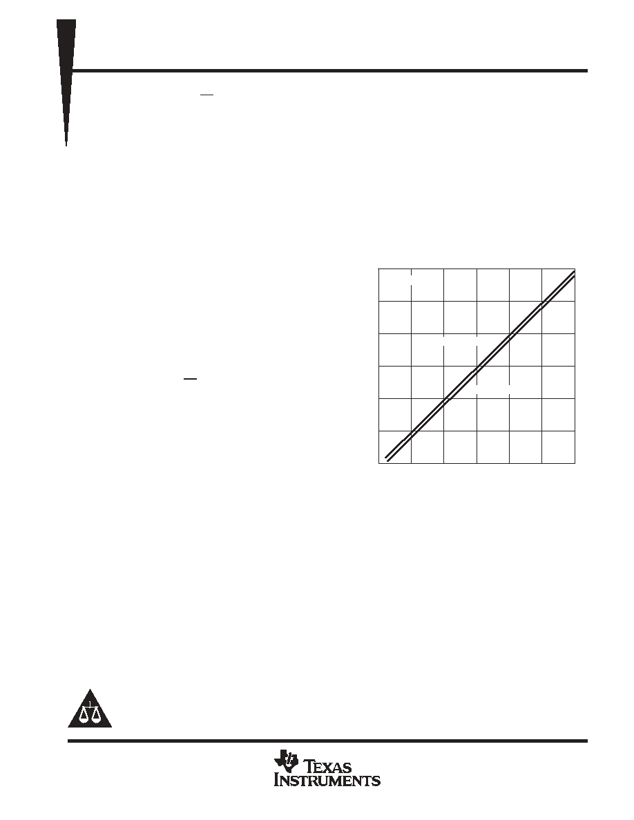
|VDD
±
| - Supply Voltage - V
10
8
6
4
4
6
8
12
14
16
10
12
14
16
MAXIMUM PEAK-TO-PEAK OUTPUT VOLTAGE
vs
SUPPLY VOLTAGE
TA = 25
∞
C
IO =
±
50
µ
A
IO =
±
500
µ
A
V(OPP) - Maximum Peak-to-Peak Output V
o
ltage - V
V
O(PP)
On products compliant to MIL PRF 38535, all parameters are tested
unless otherwise noted. On all other products, production
processing does not necessarily include testing of all parameters.

TLC227x, TLC227xA
Advanced LinCMOS RAIL TO RAIL
OPERATIONAL AMPLIFIERS
SLOS190G - FEBRUARY 1997 - REVISED MAY 2004
2
POST OFFICE BOX 655303
∑
DALLAS, TEXAS 75265
TLC2272 AVAILABLE OPTIONS
PACKAGED DEVICES
TA
VIOmax
At 25
∞
C
SMALL
OUTLINE
(D)
CERAMIC
LCC
(FK)
CERAMIC
DIP
(JG)
PLASTIC DIP
(P)
TSSOP
(PW)
CERAMIC
FLAT PACK
(U)
0
∞
C to 70
∞
C
950
µ
V
TLC2272ACD
--
--
TLC2272ACP
TLC2272ACPW
--
0
∞
C to 70
∞
C
950
µ
V
2.5 mV
TLC2272ACD
TLC2272CD
--
--
--
--
TLC2272ACP
TLC2272CP
TLC2272CPW
--
--
950
µ
V
TLC2272AID
--
--
TLC2272AIP
--
--
- 40
∞
C to 125
∞
C
950
µ
V
2.5 mV
TLC2272AID
TLC2272ID
--
--
--
--
TLC2272AIP
TLC2272IP
TLC2272IPW
--
--
- 40
∞
C to 125
∞
C
950
µ
V
TLC2272AQD
--
--
--
TLC2272AQPW
--
950
µ
V
2.5 mV
TLC2272AQD
TLC2272QD
--
--
--
--
--
TLC2272AQPW
TLC2272QPW
--
--
- 55
∞
C to 125
∞
C
950
µ
V
TLC2272AMD
TLC2272AMFK
TLC2272AMJG
TLC2272AMP
--
TLC2272AMU
- 55
∞
C to 125
∞
C
950
µ
V
2.5 mV
TLC2272AMD
TLC2272MD
TLC2272AMFK
TLC2272MFK
TLC2272AMJG
TLC2272MJG
TLC2272AMP
TLC2272MP
--
TLC2272AMU
TLC2272MU
The D packages are available taped and reeled. Add R suffix to the device type (e.g., TLC2272CDR).
The PW package is available taped and reeled. Add R suffix to the device type (e.g., TLC2272PWR).
ß Chips are tested at 25
∞
C.
TLC2274 AVAILABLE OPTIONS
PACKAGED DEVICES
TA
VIOmax
AT 25
∞
C
SMALL
OUTLINE
(D)
CERAMIC
LCC
(FK)
CERAMIC
DIP
(J)
PLASTIC
DIP
(N)
TSSOP
(PW)
CERAMIC
FLAT PACK
(W)
0
∞
C to 70
∞
C
950
µ
V
TLC2274ACD
--
--
TLC2274ACN
TLC2274ACPW
--
0
∞
C to 70
∞
C
950
µ
V
2.5 mV
TLC2274ACD
TLC2274CD
--
--
TLC2274ACN
TLC2274CN
TLC2274ACPW
TLC2274CPW
--
950
µ
V
TLC2274AID
--
--
TLC2274AIN
TLC2274AIPW
--
- 40
∞
C to 125
∞
C
950
µ
V
2.5 mV
TLC2274AID
TLC2274ID
--
--
TLC2274AIN
TLC2274IN
TLC2274AIPW
TLC2274IPW
--
- 40
∞
C to 125
∞
C
950
µ
V
TLC2274AQD
--
--
--
--
--
950
µ
V
2.5 mV
TLC2274AQD
TLC2274QD
--
--
--
--
--
- 55
∞
C to 125
∞
C
950
µ
V
TLC2274AMD
TLC2274AMFK
TLC2274AMJ
TLC2274AMN
--
TLC2274AMW
- 55
∞
C to 125
∞
C
950
µ
V
2.5 mV
TLC2274AMD
TLC2274MD
TLC2274AMFK
TLC2274MFK
TLC2274AMJ
TLC2274MJ
TLC2274AMN
TLC2274MN
--
TLC2274AMW
TLC2274MW
The D packages are available taped and reeled. Add R suffix to device type (e.g., TLC2274CDR).
The PW package is available taped and reeled.
ß Chips are tested at 25
∞
C.

TLC227x, TLC227xA
Advanced LinCMOS RAIL TO RAIL
OPERATIONAL AMPLIFIERS
SLOS190G - FEBRUARY 1997 - REVISED MAY 2004
3
POST OFFICE BOX 655303
∑
DALLAS, TEXAS 75265
1
2
3
4
8
7
6
5
1OUT
1IN -
1IN +
V
DD -
/GND
V
DD +
2OUT
2IN -
2IN +
TLC2272
D, JG, P, OR PW PACKAGE
(TOP VIEW)
1
2
3
4
5
6
7
14
13
12
11
10
9
8
1OUT
1IN -
1IN +
V
DD +
2IN +
2IN -
2OUT
4OUT
4IN -
4IN +
V
DD -
3IN +
3IN -
3OUT
3
2
1 20 19
9 10 11 12 13
4
5
6
7
8
18
17
16
15
14
4IN +
NC
V
DD -
NC
3IN +
1IN +
NC
V
DD +
NC
2IN +
1IN -
1OUT
NC
3IN -
4IN -
2IN -
2OUT
NC
NC - No internal connection
3OUT
4OUT
TLC2274
D, J, N, PW, OR W PACKAGE
(TOP VIEW)
TLC2274
FK PACKAGE
(TOP VIEW)
3
2
1 20 19
9 10 11 12 13
4
5
6
7
8
18
17
16
15
14
NC
2 OUT
NC
2 IN-
NC
NC
1 IN-
NC
1 IN+
NC
NC
1OUT
NC
NC
NC
NC
V /GND
NC
2 IN+
V
TLC2272
FK PACKAGE
(TOP VIEW)
DD-
DD+
1
2
3
4
5
10
9
8
7
6
NC
1 OUT
1 IN-
1 IN+
V
DD-
/GND
NC
V
DD+
2 OUT
2 IN-
2 IN+
TLC2272
U PACKAGE
(TOP VIEW)
TLC227x, TLC227xA
Advanced LinCMOS RAIL TO RAIL
OPERATIONAL AMPLIFIERS
SLOS190G - FEBRUARY 1997 - REVISED MAY 2004
4
POST OFFICE BOX 655303
∑
DALLAS, TEXAS 75265
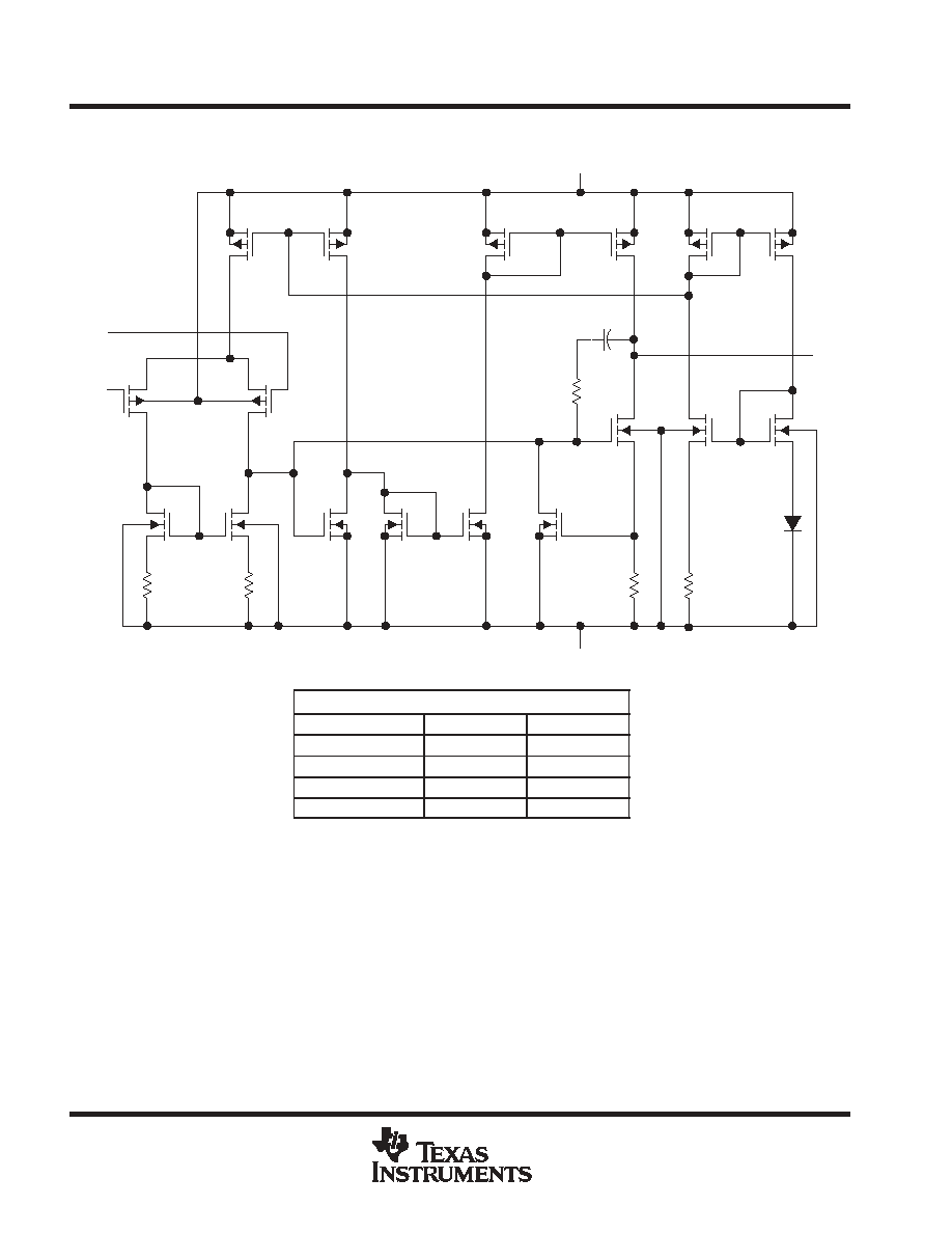
equivalent schematic (each amplifier)
Q3
Q6
Q9
Q12
Q14
Q16
Q2
Q5
Q7
Q8
Q10
Q11
D1
Q17
Q15
Q13
Q4
Q1
R5
C1
VDD +
IN +
IN -
R3
R4
R1
R2
OUT
VDD-
ACTUAL DEVICE COMPONENT COUNT
COMPONENT
TLC2272
TLC2274
Transistors
38
76
Resistors
26
52
Diodes
9
18
Capacitors
3
6
Includes both amplifiers and all ESD, bias, and trim circuitry

TLC227x, TLC227xA
Advanced LinCMOS RAIL TO RAIL
OPERATIONAL AMPLIFIERS
SLOS190G - FEBRUARY 1997 - REVISED MAY 2004
5
POST OFFICE BOX 655303
∑
DALLAS, TEXAS 75265
absolute maximum ratings over operating free-air temperature range (unless otherwise noted)
Supply voltage, V
DD +
(see Note 1)
8 V
. . . . . . . . . . . . . . . . . . . . . . . . . . . . . . . . . . . . . . . . . . . . . . . . . . . . . . . . . . . .
Supply voltage, V
DD -
(see Note 1)
-8 V
. . . . . . . . . . . . . . . . . . . . . . . . . . . . . . . . . . . . . . . . . . . . . . . . . . . . . . . . . . .
Differential input voltage, V
ID
(see Note 2)
±
16 V
. . . . . . . . . . . . . . . . . . . . . . . . . . . . . . . . . . . . . . . . . . . . . . . . . . .
Input voltage range, V
I
(any input, see Note 1)
V
DD-
- 0.3 V to V
DD+
. . . . . . . . . . . . . . . . . . . . . . . . . . . . . . . . .
Input current, I
I
(any input)
±
5 mA
. . . . . . . . . . . . . . . . . . . . . . . . . . . . . . . . . . . . . . . . . . . . . . . . . . . . . . . . . . . . . . . .
Output current, I
O
±
50 mA
. . . . . . . . . . . . . . . . . . . . . . . . . . . . . . . . . . . . . . . . . . . . . . . . . . . . . . . . . . . . . . . . . . . . . . .
Total current into V
DD +
±
50 mA
. . . . . . . . . . . . . . . . . . . . . . . . . . . . . . . . . . . . . . . . . . . . . . . . . . . . . . . . . . . . . . . . . .
Total current out of V
DD -
±
50 mA
. . . . . . . . . . . . . . . . . . . . . . . . . . . . . . . . . . . . . . . . . . . . . . . . . . . . . . . . . . . . . . . . .
Duration of short-circuit current at (or below) 25
∞
C (see Note 3)
unlimited
. . . . . . . . . . . . . . . . . . . . . . . . . . . . . .
Package thermal impedance,
JA
(see Notes 4 and 5): D package (8 pin)
97.1
∞
C/W
. . . . . . . . . . . . . . . . . . . .
D package (14 pin)
86.2
∞
C/W
. . . . . . . . . . . . . . . . . . .
N package
79.7
∞
C/W
. . . . . . . . . . . . . . . . . . . . . . . . . .
P package
84.6
∞
C/W
. . . . . . . . . . . . . . . . . . . . . . . . . .
PW package (8 pin)
149
∞
C/W
. . . . . . . . . . . . . . . . . . .
PW package (14 pin)
113
∞
C/W
. . . . . . . . . . . . . . . . . .
Package thermal impedance,
JC
(see Notes 4 and 5): FK package
5.6
∞
C/W
. . . . . . . . . . . . . . . . . . . . . . . . . . .
J package
15.1
∞
C/W
. . . . . . . . . . . . . . . . . . . . . . . . . .
U package
14.7
∞
C/W
. . . . . . . . . . . . . . . . . . . . . . . . . .
Operating free-air temperature range, T
A
: C suffix
0
∞
C to 70
∞
C
. . . . . . . . . . . . . . . . . . . . . . . . . . . . . . . . . . . . . .
I, Q suffix
-40
∞
C to 125
∞
C
. . . . . . . . . . . . . . . . . . . . . . . . . . . . . . . . .
M suffix
-55
∞
C to 125
∞
C
. . . . . . . . . . . . . . . . . . . . . . . . . . . . . . . . . .
Storage temperature range
-65
∞
C to 150
∞
C
. . . . . . . . . . . . . . . . . . . . . . . . . . . . . . . . . . . . . . . . . . . . . . . . . . . . . . . .
Lead temperature 1,6 mm (1/16 inch) from case for 10 seconds: D, N, P or PW package
260
∞
C
. . . . . . . . . .
Lead temperature 1,6 mm (1/16 inch) from case for 60 seconds: J or U package
300
∞
C
. . . . . . . . . . . . . . . . .
Stresses beyond those listed under "absolute maximum ratings" may cause permanent damage to the device. These are stress ratings only, and
functional operation of the device at these or any other conditions beyond those indicated under "recommended operating conditions" is not
implied. Exposure to absolute-maximum-rated conditions for extended periods may affect device reliability.
NOTES:
1. All voltage values, except differential voltages, are with respect to the midpoint between VDD+ and VDD -.
2. Differential voltages are at IN+ with respect to IN -. Excessive current will flow if input is brought below VDD - - 0.3 V.
3. The output may be shorted to either supply. Temperature and/or supply voltages must be limited to ensure that the maximum
dissipation rating is not exceeded.
4. Maximum power dissipation is a function of TJ(max),
JA, and TA. The maximum allowable power dissipation at any allowable
ambient temperature is PD = (TJ(max) - TA)/
JA. Operating at the absolute maximum TJ of 150
∞
C can affect reliability.
5. The package thermal impedance is calculated in accordance with JESD 51-7 (plastic) or MIL-STD-883 Method 1012 (ceramic).
recommended operating conditions
C SUFFIX
I SUFFIX
Q SUFFIX
M SUFFIX
UNIT
MIN
MAX
MIN
MAX
MIN
MAX
MIN
MAX
UNIT
Supply voltage, VDD
±
±
2.2
±
8
±
2.2
±
8
±
2.2
±
8
±
2.2
±
8
V
Input voltage, VI
VDD -
VDD + -1.5 VDD -
VDD + -1.5 VDD -
VDD + -1.5 VDD -
VDD + -1.5
V
Common-mode input voltage, VIC
VDD -
VDD + -1.5 VDD -
VDD + -1.5 VDD -
VDD + -1.5 VDD -
VDD + -1.5
V
Operating free-air temperature, TA
0
70
- 40
125
- 40
125
- 55
125
∞
C