
SN54BCT573, SN74BCT573
OCTAL TRANSPARENT D-TYPE LATCHES
WITH 3-STATE OUTPUTS
SCBS071B ≠ AUGUST 1990 ≠ REVISED MARCH 2003
1
POST OFFICE BOX 655303
∑
DALLAS, TEXAS 75265
D
Operating Voltage Range of 4.5 V to 5.5 V
D
State-of-the-Art BiCMOS Design
Significantly Reduces I
CCZ
D
Full Parallel Access for Loading
D
ESD Protection Exceeds JESD 22
≠ 2000-V Human-Body Model (A114-A)
≠ 200-V Machine Model (A115-A)
≠ 1000-V Charged-Device Model (C101)
SN54BCT573 . . . FK PACKAGE
(TOP VIEW)
SN54BCT573 . . . J OR W PACKAGE
SN74BCT573 . . . DW, N, OR NS PACKAGE
(TOP VIEW)
1
2
3
4
5
6
7
8
9
10
20
19
18
17
16
15
14
13
12
11
OE
1D
2D
3D
4D
5D
6D
7D
8D
GND
V
CC
1Q
2Q
3Q
4Q
5Q
6Q
7Q
8Q
LE
3
2
1 20 19
9 10 11 12 13
4
5
6
7
8
18
17
16
15
14
2Q
3Q
4Q
5Q
6Q
3D
4D
5D
6D
7D
2D
1D
OE
8Q
7Q
1Q
8D
GND
LE
V
CC
description/ordering information
These 8-bit latches feature 3-state outputs designed specifically for driving highly capacitive or relatively
low-impedance loads. They are particularly suitable for implementing buffer registers, I/O ports, bidirectional
bus drivers, and working registers.
The eight latches of the 'BCT573 devices are transparent D-type latches. While the latch-enable (LE) input is
high, the Q outputs follow the data (D) inputs. When the latch enable is taken low, the Q outputs are latched
at the logic levels that were set up at the D inputs.
A buffered output-enable (OE) input can be used to place the eight outputs in either a normal logic state (high
or low logic levels) or the high-impedance state. In the high-impedance state, the outputs neither load nor drive
the bus lines significantly. The high-impedance state and increased drive provide the capability to drive bus
lines without interface or pullup components.
To ensure the high-impedance state during power up or power down, OE should be tied to V
CC
through a pullup
resistor; the minimum value of the resistor is determined by the current-sinking capability of the driver.
OE does not affect internal operations of the latches. Old data can be retained or new data can be entered while
the outputs are in the high-impedance state.
ORDERING INFORMATION
TA
PACKAGE
ORDERABLE
PART NUMBER
TOP-SIDE
MARKING
PDIP ≠ N
Tube
SN74BCT573N
SN74BCT573N
0
∞
C to 70
∞
C
SOIC
DW
Tube
SN74BCT573DW
BCT573
0
∞
C to 70
∞
C
SOIC ≠ DW
Tape and reel
SN74BCT573DWR
BCT573
SOP ≠ NS
Tape and reel
SN74BCT573NSR
BCT573
CDIP ≠ J
Tube
SNJ54BCT573J
SNJ54BCT573J
≠55
∞
C to 125
∞
C
CFP ≠ W
Tube
SNJ54BCT573W
SNJ54BCT573W
LCCC ≠ FK
Tube
SNJ54BCT573FK
SNJ54BCT573FK
Package drawings, standard packing quantities, thermal data, symbolization, and PCB design guidelines are
available at www.ti.com/sc/package.
Copyright
2003, Texas Instruments Incorporated
Please be aware that an important notice concerning availability, standard warranty, and use in critical applications of
Texas Instruments semiconductor products and disclaimers thereto appears at the end of this data sheet.
PRODUCTION DATA information is current as of publication date.
Products conform to specifications per the terms of Texas Instruments
standard warranty. Production processing does not necessarily include
testing of all parameters.
On products compliant to MIL-PRF-38535, all parameters are tested
unless otherwise noted. On all other products, production
processing does not necessarily include testing of all parameters.

SN54BCT573, SN74BCT573
OCTAL TRANSPARENT D-TYPE LATCHES
WITH 3-STATE OUTPUTS
SCBS071B ≠ AUGUST 1990 ≠ REVISED MARCH 2003
2
POST OFFICE BOX 655303
∑
DALLAS, TEXAS 75265
FUNCTION TABLE
(each latch)
INPUTS
OUTPUT
OE
LE
D
Q
L
H
H
H
L
H
L
L
L
L
X
Q0
H
X
X
Z
logic diagram (positive logic)
OE
LE
1D
1Q
1
11
2
19
To Seven Other Channels
C1
1D
absolute maximum ratings over operating free-air temperature range (unless otherwise noted)
Supply voltage range, V
CC
≠0.5 V to 7 V
. . . . . . . . . . . . . . . . . . . . . . . . . . . . . . . . . . . . . . . . . . . . . . . . . . . . . . . . . .
Input voltage range, V
I
(see Note 1)
≠0.5 V to 7 V
. . . . . . . . . . . . . . . . . . . . . . . . . . . . . . . . . . . . . . . . . . . . . . . . . .
Voltage range applied to any output in the disabled or power-off state, V
O
≠0.5 V to 5.5 V
. . . . . . . . . . . . . . . .
Voltage range applied to any output in the high state, V
O
≠0.5 V to V
CC
. . . . . . . . . . . . . . . . . . . . . . . . . . . . . . .
Input clamp current, I
IK
(V
I
< 0)
≠30 mA
. . . . . . . . . . . . . . . . . . . . . . . . . . . . . . . . . . . . . . . . . . . . . . . . . . . . . . . . . . .
Current into any output in the low state: SN54BCT573
96 mA
. . . . . . . . . . . . . . . . . . . . . . . . . . . . . . . . . . . . . . .
SN74BCT573 128
mA
. . . . . . . . . . . . . . . . . . . . . . . . . . . . . . . . . . . . . .
Package thermal impedance,
JA
(see Note 2): DW package
58
∞
C/W
. . . . . . . . . . . . . . . . . . . . . . . . . . . . . . . . .
N package
69
∞
C/W
. . . . . . . . . . . . . . . . . . . . . . . . . . . . . . . . . . .
NS package
60
∞
C/W
. . . . . . . . . . . . . . . . . . . . . . . . . . . . . . . . .
Storage temperature range, T
stg
≠65
∞
C to 150
∞
C
. . . . . . . . . . . . . . . . . . . . . . . . . . . . . . . . . . . . . . . . . . . . . . . . . . .
Stresses beyond those listed under "absolute maximum ratings" may cause permanent damage to the device. These are stress ratings only, and
functional operation of the device at these or any other conditions beyond those indicated under "recommended operating conditions" is not
implied. Exposure to absolute-maximum-rated conditions for extended periods may affect device reliability.
NOTES:
1. The input and output voltage ratings may be exceeded if the input and output current ratings are observed.
2. The package thermal impedance is calculated in accordance with JESD 51-7.

SN54BCT573, SN74BCT573
OCTAL TRANSPARENT D-TYPE LATCHES
WITH 3-STATE OUTPUTS
SCBS071B ≠ AUGUST 1990 ≠ REVISED MARCH 2003
3
POST OFFICE BOX 655303
∑
DALLAS, TEXAS 75265
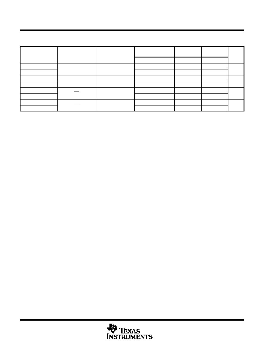
recommended operating conditions (see Note 3)
SN54BCT573
SN74BCT573
UNIT
MIN
NOM
MAX
MIN
NOM
MAX
UNIT
VCC
Supply voltage
4.5
5
5.5
4.5
5
5.5
V
VIH
High-level input voltage
2
2
V
VIL
Low-level input voltage
0.8
0.8
V
IIK
Input clamp current
≠18
≠18
mA
IOH
High-level output current
≠12
≠15
mA
IOL
Low-level output current
48
64
mA
TA
Operating free-air temperature
≠55
125
0
70
∞
C
NOTE 3: All unused inputs of the device must be held at VCC or GND to ensure proper device operation. Refer to the TI application report,
Implications of Slow or Floating CMOS Inputs, literature number SCBA004.
electrical characteristics over recommended operating free-air temperature range (unless
otherwise noted)
PARAMETER
TEST CONDITIONS
SN54BCT573
SN74BCT573
UNIT
PARAMETER
TEST CONDITIONS
MIN
TYP
MAX
MIN
TYP
MAX
UNIT
VIK
VCC = 4.5 V,
II = ≠18 mA
≠1.2
≠1.2
V
IOH = ≠3 mA
2.4
3.3
2.4
3.3
VOH
VCC = 4.5 V
IOH = ≠12 mA
2
3.2
V
IOH = ≠15 mA
2
3.1
VOL
VCC = 4 5 V
IOL = 48 mA
0.38
0.55
V
VOL
VCC = 4.5 V
IOL = 64 mA
0.42
0.55
V
II
VCC = 5.5 V,
VI = 5.5 V
0.4
0.4
mA
IIH
VCC = 5.5 V,
VI = 2.7 V
20
20
µ
A
IIL
VCC = 5.5 V,
VI = 0.5 V
≠0.6
≠0.6
mA
IOS
VCC = 5.5 V,
VO = 0
≠100
≠225
≠100
≠225
mA
IOZH
VCC = 5.5 V,
VO = 2.7 V
50
50
µ
A
IOZL
VCC = 5.5 V,
VO = 0.5 V
≠50
≠50
µ
A
ICCL
VCC = 5.5 V,
Outputs open
62
62
mA
ICCH
VCC = 5.5 V,
Outputs open
8
8
mA
ICCZ
VCC = 5.5 V,
Outputs open
8
8
mA
Ci
VCC = 5 V,
VI = 2.5 V or 0.5 V
5.5
5.5
pF
Co
VCC = 5 V,
VO = 2.5 V or 0.5 V
7.5
7.5
pF
All typical values are at VCC = 5 V, TA = 25
∞
C.
Not more than one output should be tested at a time, and the duration of the test should not exceed one second.
timing requirements over recommended ranges of supply voltage and operating free-air
temperature (unless otherwise noted)
VCC = 5 V,
TA = 25
∞
C
SN54BCT573
SN74BCT573
UNIT
MIN
MAX
MIN
MAX
MIN
MAX
tw
Pulse duration, LE high
4
4
4
ns
tsu
Setup time, data before LE
1
2.5
1
ns
th
Hold time, data after LE
4
4
4
ns
SN54BCT573, SN74BCT573
OCTAL TRANSPARENT D-TYPE LATCHES
WITH 3-STATE OUTPUTS
SCBS071B ≠ AUGUST 1990 ≠ REVISED MARCH 2003
4
POST OFFICE BOX 655303
∑
DALLAS, TEXAS 75265
switching characteristics over recommended ranges of supply voltage and operating free-air
temperature, C
L
= 50 pF (unless otherwise noted) (see Figure 1)
PARAMETER
FROM
(INPUT)
TO
(OUTPUT)
VCC = 5 V,
TA = 25
∞
C
SN54BCT573
SN74BCT573
UNIT
(INPUT)
(OUTPUT)
MIN
TYP
MAX
MIN
MAX
MIN
MAX
tPLH
D
Q
2
5
7.2
1
9.8
2
8.4
ns
tPHL
D
Q
2.8
5.9
8.2
1.5
10.3
2.8
9.6
ns
tPLH
LE
Q
2.4
6.1
7.2
2
9.7
2.4
8.1
ns
tPHL
LE
Q
2.9
5.2
7.1
2
8.8
2.9
7.8
ns
tPZH
OE
Q
3
6.2
8.5
2.5
11
3
10.4
ns
tPZL
OE
Q
4.3
7.1
9.3
3.5
11.5
4.3
11
ns
tPHZ
OE
Q
2.2
3.9
5.6
1.5
7.2
2.2
6
ns
tPLZ
OE
Q
1.7
3.6
5.2
1
7
1.7
6
ns

SN54BCT573, SN74BCT573
OCTAL TRANSPARENT D-TYPE LATCHES
WITH 3-STATE OUTPUTS
SCBS071B ≠ AUGUST 1990 ≠ REVISED MARCH 2003
5
POST OFFICE BOX 655303
∑
DALLAS, TEXAS 75265
PARAMETER MEASUREMENT INFORMATION
NOTES: A. CL includes probe and jig capacitance.
B. All input pulses are supplied by generators having the following characteristics: PRR
10 MHz, tr = tf
2.5 ns, duty cycle = 50%.
C. Waveform 1 is for an output with internal conditions such that the output is low except when disabled by the output control.
Waveform 2 is for an output with internal conditions such that the output is high except when disabled by the output control.
D. The outputs are measured one at a time with one transition per measurement.
E. When measuring propagation delay times of 3-state outputs, switch S1 is open.
F. All parameters and waveforms are not applicable to all devices.
From Output
Under Test
Test
Point
R1
CL
(see Note A)
LOAD CIRCUIT FOR
TOTEM-POLE OUTPUTS
LOAD CIRCUIT FOR
3-STATE AND OPEN-COLLECTOR OUTPUTS
R1
S1
7 V (tPZL, tPLZ, O.C.)
Open
(all others)
From Output
Under Test
Test
Point
R2
CL
(see Note A)
RL = R1 = R2
1.5 V
1.5 V
1.5 V
3 V
3 V
0 V
0 V
th
tsu
VOLTAGE WAVEFORMS
SETUP AND HOLD TIMES
Timing Input
(see Note B)
Data Input
(see Note B)
1.5 V
1.5 V
3 V
3 V
0 V
0 V
High-Level
Pulse
(see Note B)
Low-Level
Pulse
tw
VOLTAGE WAVEFORMS
PULSE DURATION
1.5 V
1.5 V
tPHL
tPLH
tPLH
tPHL
Input
(see Note B)
Out-of-Phase
Output
(see Note D)
1.5 V
1.5 V
1.5 V
1.5 V
1.5 V
1.5 V
3 V
0 V
VOL
VOH
VOH
VOL
In-Phase
Output
(see Note D)
VOLTAGE WAVEFORMS
PROPAGATION DELAY TIMES (see Note D)
tPHZ
tPLZ
0.3 V
tPZL
tPZH
1.5 V
1.5 V
1.5 V
1.5 V
3 V
0 V
Output
Control
(low-level enable)
Waveform 1
(see Notes C and D)
Waveform 2
(see Notes C and D)
0 V
VOH
VOL
3.5 V
0.3 V
VOLTAGE WAVEFORMS
ENABLE AND DISABLE TIMES, 3-STATE OUTPUTS
Figure 1. Load Circuit and Voltage Waveforms

MECHANICAL DATA
MCFP006B - JANUARY 1995 - REVISED JULY 2003
1
POST OFFICE BOX 655303
∑
DALLAS, TEXAS 75265
W (R-GDFP-F20)
CERAMIC DUAL FLATPACK
10
11
0.250 (6,35)
0.370 (9,40)
20
1
0.245 (6,22)
0.004 (0,10)
0.026 (0,66)
4 Places
0.015 (0,38)
0.045 (1,14)
0.009 (0,23)
0.045 (1,14)
Base and Seating Plane
0.005 (0,13) MIN
0.022 (0,56)
0.300 (7,62)
0.100 (2,54)
4040180-4 /D 07/03
0.320 (8,13) MAX
0.250 (6,35)
0.370 (9,40)
0.540 (13,72)
MAX
0.050 (1,27)
NOTES: A. All linear dimensions are in inches (millimeters).
B. This drawing is subject to change without notice.
C. This package can be hermetically sealed with a ceramic lid using glass frit.
D. Index point is provided on cap for terminal identification only.
E. Falls within Mil-Std 1835 GDFP2-F20

MECHANICAL DATA
MLCC006B ≠ OCTOBER 1996
1
POST OFFICE BOX 655303
∑
DALLAS, TEXAS 75265
FK (S-CQCC-N**)
LEADLESS CERAMIC CHIP CARRIER
4040140 / D 10/96
28 TERMINAL SHOWN
B
0.358
(9,09)
MAX
(11,63)
0.560
(14,22)
0.560
0.458
0.858
(21,8)
1.063
(27,0)
(14,22)
A
NO. OF
MIN
MAX
0.358
0.660
0.761
0.458
0.342
(8,69)
MIN
(11,23)
(16,26)
0.640
0.739
0.442
(9,09)
(11,63)
(16,76)
0.962
1.165
(23,83)
0.938
(28,99)
1.141
(24,43)
(29,59)
(19,32)
(18,78)
**
20
28
52
44
68
84
0.020 (0,51)
TERMINALS
0.080 (2,03)
0.064 (1,63)
(7,80)
0.307
(10,31)
0.406
(12,58)
0.495
(12,58)
0.495
(21,6)
0.850
(26,6)
1.047
0.045 (1,14)
0.045 (1,14)
0.035 (0,89)
0.035 (0,89)
0.010 (0,25)
12
13
14
15
16
18
17
11
10
8
9
7
5
4
3
2
0.020 (0,51)
0.010 (0,25)
6
1
28
26
27
19
21
B SQ
A SQ
22
23
24
25
20
0.055 (1,40)
0.045 (1,14)
0.028 (0,71)
0.022 (0,54)
0.050 (1,27)
NOTES: A. All linear dimensions are in inches (millimeters).
B. This drawing is subject to change without notice.
C. This package can be hermetically sealed with a metal lid.
D. The terminals are gold plated.
E. Falls within JEDEC MS-004

MECHANICAL
MPDI002C ≠ JANUARY 1995 ≠ REVISED DECEMBER 20002
1
POST OFFICE BOX 655303
∑
DALLAS, TEXAS 75265
N (R-PDIP-T**)
PLASTIC DUAL-IN-LINE PACKAGE
BB
AC
AD
0.325 (8,26)
0.300 (7,62)
0.010 (0,25) NOM
Gauge Plane
0.015 (0,38)
0.430 (10,92) MAX
20
1.060
(26,92)
0.940
(23,88)
18
0.920
0.850
14
0.775
0.745
(19,69)
(18,92)
16
0.775
(19,69)
(18,92)
0.745
A MIN
DIM
A MAX
PINS **
(23,37)
(21,59)
Seating Plane
14/18 PIN ONLY
20 pin vendor option
4040049/E 12/2002
9
8
0.070 (1,78)
A
0.045 (1,14)
0.020 (0,51) MIN
16
1
0.015 (0,38)
0.021 (0,53)
0.200 (5,08) MAX
0.125 (3,18) MIN
0.240 (6,10)
0.260 (6,60)
M
0.010 (0,25)
0.100 (2,54)
16 PINS SHOWN
MS-100
VARIATION
AA
C
D
D
D
0.030 (0,76)
0.045 (1,14)
NOTES: A. All linear dimensions are in inches (millimeters).
B. This drawing is subject to change without notice.
C. Falls within JEDEC MS-001, except 18 and 20 pin minimum body lrngth (Dim A).
D. The 20 pin end lead shoulder width is a vendor option, either half or full width.

MECHANICAL DATA
MSOI003E ≠ JANUARY 1995 ≠ REVISED SEPTEMBER 2001
1
POST OFFICE BOX 655303
∑
DALLAS, TEXAS 75265
DW (R-PDSO-G**)
PLASTIC SMALL-OUTLINE PACKAGE
16 PINS SHOWN
0.419 (10,65)
0.400 (10,15)
0.291 (7,39)
0.299 (7,59)
16
0.400
(10,16)
A MIN
A MAX
(10,41)
0.410
0.462
(11,73)
(11,51)
0.453
18
0.610
(15,49)
(15,24)
0.600
24
DIM
PINS **
4040000/E 08/01
0.104 (2,65) MAX
0.004 (0,10)
0.012 (0,30)
Seating Plane
0
∞
≠ 8
∞
0.016 (0,40)
0.050 (1,27)
16
0.050 (1,27)
1
A
8
9
0.014 (0,35)
0.020 (0,51)
0.010 (0,25) NOM
Gage Plane
0.010 (0,25)
28
0.710
(18,03)
0.700
(17,78)
(12,70)
(12,95)
0.500
20
0.510
0.010 (0,25)
0.004 (0,10)
NOTES: A. All linear dimensions are in inches (millimeters).
B. This drawing is subject to change without notice.
C. Body dimensions do not include mold flash or protrusion not to exceed 0.006 (0,15).
D. Falls within JEDEC MS-013


IMPORTANT NOTICE
Texas Instruments Incorporated and its subsidiaries (TI) reserve the right to make corrections, modifications,
enhancements, improvements, and other changes to its products and services at any time and to discontinue
any product or service without notice. Customers should obtain the latest relevant information before placing
orders and should verify that such information is current and complete. All products are sold subject to TI's terms
and conditions of sale supplied at the time of order acknowledgment.
TI warrants performance of its hardware products to the specifications applicable at the time of sale in
accordance with TI's standard warranty. Testing and other quality control techniques are used to the extent TI
deems necessary to support this warranty. Except where mandated by government requirements, testing of all
parameters of each product is not necessarily performed.
TI assumes no liability for applications assistance or customer product design. Customers are responsible for
their products and applications using TI components. To minimize the risks associated with customer products
and applications, customers should provide adequate design and operating safeguards.
TI does not warrant or represent that any license, either express or implied, is granted under any TI patent right,
copyright, mask work right, or other TI intellectual property right relating to any combination, machine, or process
in which TI products or services are used. Information published by TI regarding third-party products or services
does not constitute a license from TI to use such products or services or a warranty or endorsement thereof.
Use of such information may require a license from a third party under the patents or other intellectual property
of the third party, or a license from TI under the patents or other intellectual property of TI.
Reproduction of information in TI data books or data sheets is permissible only if reproduction is without
alteration and is accompanied by all associated warranties, conditions, limitations, and notices. Reproduction
of this information with alteration is an unfair and deceptive business practice. TI is not responsible or liable for
such altered documentation.
Resale of TI products or services with statements different from or beyond the parameters stated by TI for that
product or service voids all express and any implied warranties for the associated TI product or service and
is an unfair and deceptive business practice. TI is not responsible or liable for any such statements.
Following are URLs where you can obtain information on other Texas Instruments products and application
solutions:
Products
Applications
Amplifiers
amplifier.ti.com
Audio
www.ti.com/audio
Data Converters
dataconverter.ti.com
Automotive
www.ti.com/automotive
DSP
dsp.ti.com
Broadband
www.ti.com/broadband
Interface
interface.ti.com
Digital Control
www.ti.com/digitalcontrol
Logic
logic.ti.com
Military
www.ti.com/military
Power Mgmt
power.ti.com
Optical Networking
www.ti.com/opticalnetwork
Microcontrollers
microcontroller.ti.com
Security
www.ti.com/security
Telephony
www.ti.com/telephony
Video & Imaging
www.ti.com/video
Wireless
www.ti.com/wireless
Mailing Address:
Texas Instruments
Post Office Box 655303 Dallas, Texas 75265
Copyright
2003, Texas Instruments Incorporated