Äîêóìåíòàöèÿ è îïèñàíèÿ www.docs.chipfind.ru
SN5414, SN54LS14,
SN7414, SN74LS14
HEX SCHMITT-TRIGGER INVERTERS
SDLS049B DECEMBER 1983 REVISED FEBRUARY 2002
1
POST OFFICE BOX 655303
·
DALLAS, TEXAS 75265
D
Operation From Very Slow Edges
D
Improved Line-Receiving Characteristics
D
High Noise Immunity
description
Each circuit functions as an inverter, but because
of the Schmitt action, it has different input
threshold levels for positive-going (V
T+
) and
negative-going (V
T
) signals.
These circuits are temperature compensated and
can be triggered from the slowest of input ramps
and still give clean, jitter-free output signals.
ORDERING INFORMATION
TA
PACKAGE
ORDERABLE
PART NUMBER
TOP-SIDE
MARKING
PDIP
N
Tube
SN7414N
SN7414N
PDIP N
Tube
SN74LS14N
SN74LS14N
Tube
SN7414D
7414
0
°
C to 70
°
C
SOIC
D
Tape and reel
SN7414DR
7414
0
°
C to 70
°
C
SOIC D
Tube
SN74LS14D
LS14
Tape and reel
SN74LS14DR
LS14
SOP NS
Tape and reel
SN7414NSR
SN7414
SSOP DB
Tape and reel
SN74LS14DBR
LS14
Tube
SN5414J
SN5414J
CDIP
J
Tube
SNJ5414J
SNJ5414J
CDIP J
Tube
SN54LS14J
SN54LS14J
55
°
C to 125
°
C
Tube
SNJ54LS14J
SNJ54LS14J
CFP
W
Tube
SNJ5414W
SNJ5414W
CFP W
Tube
SNJ54LS14W
SNJ54LS14W
LCCC FK
Tube
SNJ54LS14FK
SNJ54LS14FK
Package drawings, standard packing quantities, thermal data, symbolization, and PCB design guidelines are
available at www.ti.com/sc/package.
Copyright
2002, Texas Instruments Incorporated
PRODUCTION DATA information is current as of publication date.
Products conform to specifications per the terms of Texas Instruments
standard warranty. Production processing does not necessarily include
testing of all parameters.
Please be aware that an important notice concerning availability, standard warranty, and use in critical applications of
Texas Instruments semiconductor products and disclaimers thereto appears at the end of this data sheet.
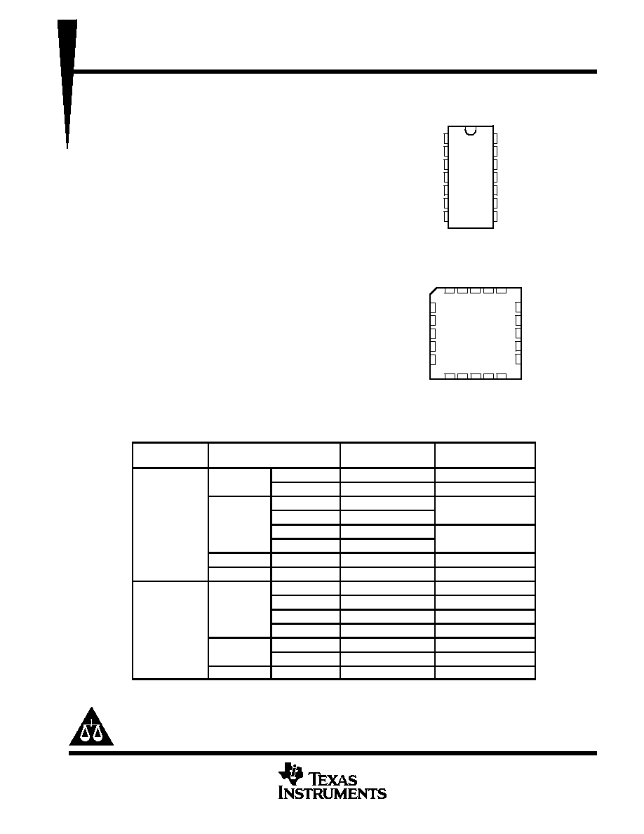
SN5414, SN54LS14 . . . J OR W PACKAGE
SN7414 . . . D, N, OR NS PACKAGE
SN74LS14 . . . D, DB, OR N PACKAGE
(TOP VIEW)
1
2
3
4
5
6
7
14
13
12
11
10
9
8
1A
1Y
2A
2Y
3A
3Y
GND
V
CC
6A
6Y
5A
5Y
4A
4Y
3
2
1 20 19
9 10 11 12 13
4
5
6
7
8
18
17
16
15
14
6Y
NC
5A
NC
5Y
2A
NC
2Y
NC
3A
1Y
1A
NC
4Y
4A
6A
3Y
GND
NC
NC No internal connection
V
CC
SN54LS14 . . . FK PACKAGE
(TOP VIEW)
On products compliant to MIL-PRF-38535, all parameters are tested
unless otherwise noted. On all other products, production
processing does not necessarily include testing of all parameters.
SN5414, SN54LS14,
SN7414, SN74LS14
HEX SCHMITT-TRIGGER INVERTERS
SDLS049B DECEMBER 1983 REVISED FEBRUARY 2002
2
POST OFFICE BOX 655303
·
DALLAS, TEXAS 75265
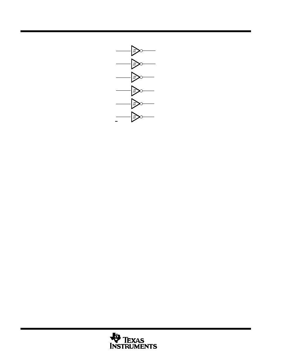
logic diagram (positive logic)
1A
2A
3A
4A
5A
6A
1Y
2Y
3Y
4Y
5Y
6Y
1
3
5
9
11
13
2
4
6
8
10
12
Y = A
Pin numbers shown are for the D, DB, J, N, NS, and W packages.
SN5414, SN54LS14,
SN7414, SN74LS14
HEX SCHMITT-TRIGGER INVERTERS
SDLS049B DECEMBER 1983 REVISED FEBRUARY 2002
3
POST OFFICE BOX 655303
·
DALLAS, TEXAS 75265
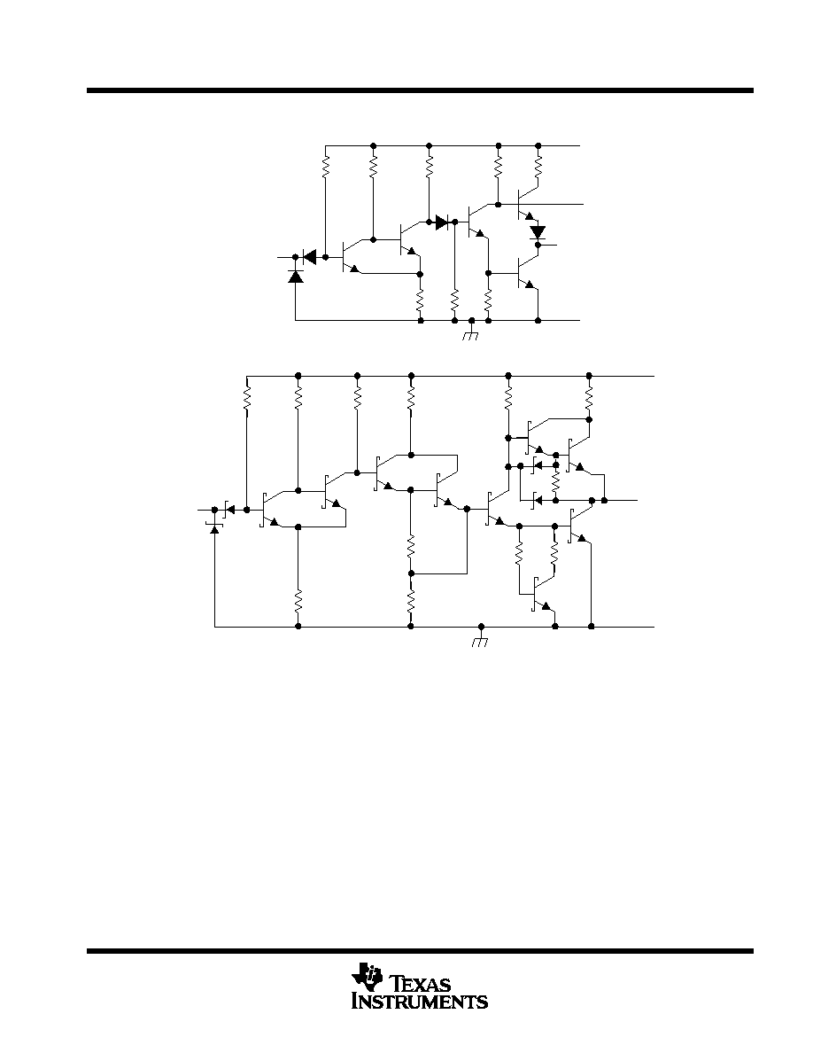
schematic
'14
GND
Output Y
100
VCC
6 k
Input A
GND
Output Y
VCC
20 k
Input A
'LS14
Resistor values shown are nominal.
SN5414, SN54LS14,
SN7414, SN74LS14
HEX SCHMITT-TRIGGER INVERTERS
SDLS049B DECEMBER 1983 REVISED FEBRUARY 2002
4
POST OFFICE BOX 655303
·
DALLAS, TEXAS 75265
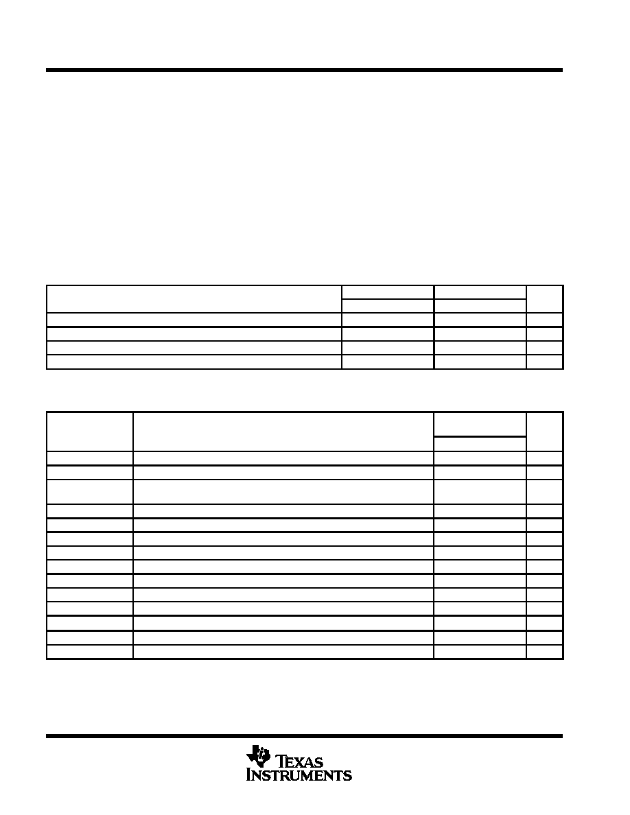
absolute maximum ratings over operating free-air temperature (unless otherwise noted)
Supply voltage, V
CC
(see Note 1)
7 V
. . . . . . . . . . . . . . . . . . . . . . . . . . . . . . . . . . . . . . . . . . . . . . . . . . . . . . . . . . . . .
Input voltage: '14
5.5 V
. . . . . . . . . . . . . . . . . . . . . . . . . . . . . . . . . . . . . . . . . . . . . . . . . . . . . . . . . . . . . . . . . . . . . . . . .
'LS14
7 V
. . . . . . . . . . . . . . . . . . . . . . . . . . . . . . . . . . . . . . . . . . . . . . . . . . . . . . . . . . . . . . . . . . . . . . . . .
Package thermal impedance,
JA
(see Note 2): D package
86
°
C/W
. . . . . . . . . . . . . . . . . . . . . . . . . . . . . . . . . . .
DB package
96
°
C/W
. . . . . . . . . . . . . . . . . . . . . . . . . . . . . . . . . .
N package
80
°
C/W
. . . . . . . . . . . . . . . . . . . . . . . . . . . . . . . . . . .
NS package
76
°
C/W
. . . . . . . . . . . . . . . . . . . . . . . . . . . . . . . . . .
Storage temperaturerange, T
stg
65
°
C to 150
°
C
. . . . . . . . . . . . . . . . . . . . . . . . . . . . . . . . . . . . . . . . . . . . . . . . . . .
Stresses beyond those listed under "absolute maximum ratings" may cause permanent damage to the device. These are stress ratings only, and
functional operation of the device at these or any other conditions beyond those indicated under "recommended operating conditions" is not
implied. Exposure to absolute-maximum-rated conditions for extended periods may affect device reliability.
NOTES:
1. Voltage values are with respect to network ground terminal.
2. The package termal impedance is calculated in accordance with JESD 51-7
recommended operating conditions
SN5414
SN7414
UNIT
MIN
NOM
MAX
MIN
NOM
MAX
UNIT
VCC
Supply voltage
4.5
5
5.5
4.75
5
5.25
V
IOH
High-level output current
0.8
0.8
mA
IOL
Low-level output current
16
16
mA
TA
Operating free-air temperature
55
125
0
70
°
C
electrical characteristics over recommended operating free-air temperature range (unless
otherwise noted)
PARAMETER
TEST CONDITIONS
SN5414
SN7414
UNIT
TEST CONDITIONS
MIN
TYP§
MAX
VT+
VCC = 5 V
1.5
1.7
2
V
VT
VCC = 5 V
0.6
0.9
1.1
V
Hysteresis
(VT+ VT)
VCC = 5 V
0.4
0.8
V
VIK
VCC = MIN,
II = 12 mA
1.5
V
VOH
VCC = MIN,
VI = 0.6 V,
IOH = 0.8 mA
2.4
3.4
V
VOL
VCC = MIN,
VI = 2 V,
IOL = 16 mA
0.2
0.4
V
IT+
VCC = 5 V,
VI = VT+
0.43
mA
IT
VCC = 5 V,
VI = VT
0.56
mA
II
VCC = MAX,
VI = 5.5 V
1
mA
IIH
VCC = MAX,
VIH = 2.4 V
40
µ
A
IIL
VCC = MAX,
VIL = 0.4 V
0.8
1.2
mA
IOS¶
VCC = MAX
18
55
mA
ICCH
VCC = MAX
22
36
mA
ICCL
VCC = MAX
39
60
mA
For conditions shown as MIN or MAX, use the appropriate value specified under recommended operating conditions.
§ All typical values are at VCC = 5 V, TA = 25
°
C.
¶ Not more than one output should be shorted at a time.
SN5414, SN54LS14,
SN7414, SN74LS14
HEX SCHMITT-TRIGGER INVERTERS
SDLS049B DECEMBER 1983 REVISED FEBRUARY 2002
5
POST OFFICE BOX 655303
·
DALLAS, TEXAS 75265
switching characteristics, V
CC
= 5 V, T
A
= 25
°
C (see Figure 1)
PARAMETER
FROM
(INPUT)
TO
(OUTPUT)
TEST CONDITIONS
SN5414
SN7414
UNIT
PARAMETER
(INPUT)
(OUTPUT)
TEST CONDITIONS
MIN
TYP
MAX
UNIT
MIN
TYP
MAX
tPLH
A
Y
RL = 400
CL = 15 pF
15
22
ns
tPHL
A
Y
RL = 400
,
CL = 15 F
15
22
ns
recommended operating conditions
SN54LS14
SN74LS14
UNIT
MIN
NOM
MAX
MIN
NOM
MAX
UNIT
VCC
Supply voltage
4.5
5
5.5
4.75
5
5.25
V
IOH
High-level output current
0.4
0.4
mA
IOL
Low-level output current
4
8
mA
TA
Operating free-air temperature
55
125
0
70
°
C
electrical characteristics over recommended operating free-air temperature range (unless
otherwise noted)
PARAMETER
TEST CONDITIONS
SN54LS14
SN74LS14
UNIT
PARAMETER
TEST CONDITIONS
MIN
TYP
MAX
MIN
TYP
MAX
UNIT
VT+
VCC = 5 V
1.4
1.6
1.9
1.4
1.6
1.9
V
VT
VCC = 5 V
0.5
0.8
1
0.5
0.8
1
V
Hysteresis
(VT+ VT)
VCC = 5 V
0.4
0.8
0.4
0.8
V
VIK
VCC = MIN,
II = 18 mA
1.5
1.5
V
VOH
VCC = MIN,
VI = 0.5 V,
IOH = 0.4 mA
2.5
3.4
2.7
3.4
V
VOL
VCC = MIN
VI = 1 9 V
IOL= 4 mA
0.25
0.4
0.25
0.4
V
VOL
VCC = MIN,
VI = 1.9 V
IOL = 8 mA
0.35
0.5
V
IT+
VCC = 5 V,
VI = VT+
0.14
0.14
mA
IT
VCC = 5 V,
VI = VT
0.18
0.18
mA
II
VCC = MAX,
VI = 7 V
0.1
0.1
mA
IIH
VCC = MAX,
VIH = 2.7 V
20
20
µ
A
IIL
VCC = MAX,
VIL = 0.4 V
0.4
0.4
mA
IOS§
VCC = MAX
20
100
20
100
mA
ICCH
VCC = MAX
8.6
16
8.6
16
mA
ICCL
VCC = MAX
12
21
12
21
mA
For conditions shown as MIN or MAX, use the appropriate value specified under recommended operating conditions.
All typical values are at VCC = 5 V, TA = 25
°
C.
§ Not more than one output should be shorted at a time, and duration of the short-circuit should not exceed one second.
switching characteristics, V
CC
= 5 V, T
A
= 25
°
C (see Figure 2)
PARAMETER
FROM
TO
TEST CONDITIONS
MIN
TYP
MAX
UNIT
PARAMETER
(INPUT)
(OUTPUT)
TEST CONDITIONS
MIN
TYP
MAX
UNIT
tPLH
A
Y
RL = 2 k
CL = 15 pF
15
22
ns
tPHL
A
Y
RL = 2 k
,
CL = 15 F
15
22
ns