
SN54ABT853, SN74ABT853
8-BIT TO 9-BIT PARITY BUS TRANSCEIVERS
SCBS198F ≠ FEBRUARY 1991 ≠ REVISED OCTOBER 1997
1
POST OFFICE BOX 655303
∑
DALLAS, TEXAS 75265
D
State-of-the-Art
EPIC-
B
TM
BiCMOS Design
Significantly Reduces Power Dissipation
D
ESD Protection Exceeds 2000 V Per
MIL-STD-883, Method 3015; Exceeds 200 V
Using Machine Model (C = 200 pF, R = 0)
D
Latch-Up Performance Exceeds 500 mA Per
JESD 17
D
Typical V
OLP
(Output Ground Bounce)
< 1 V at V
CC
= 5 V, T
A
= 25
∞
C
D
High-Drive Outputs (≠32-mA I
OH
, 64-mA I
OL
)
D
High-Impedance State During Power Up
and Power Down
D
Parity-Error Flag With Parity
Generator/Checker
D
Latch for Storage of Parity-Error Flag
D
Package Options Include Plastic
Small-Outline (DW), Shrink Small-Outline
(DB), and Thin Shrink Small-Outline (PW)
Packages, Ceramic Chip Carriers (FK),
Ceramic Flat (W) Package, and Plastic (NT)
and Ceramic (JT) DIPs
description
The 'ABT853 8-bit to 9-bit parity transceivers are
designed for communication between data buses.
When data is transmitted from the A bus to the
B bus, a parity bit is generated. When data is
transmitted from the B bus to the A bus with its
corresponding parity bit, the open-collector
parity-error (ERR) output indicates whether or not
an error in the B data has occurred. The
output-enable (OEA and OEB) inputs can be used
to disable the device so that the buses are
effectively isolated. The 'ABT853 transceivers
provide true data at their outputs.
A 9-bit parity generator/checker generates a parity-odd (PARITY) output and monitors the parity of the I/O ports
with the ERR flag. The parity-error output can be passed, sampled, stored, or cleared from the latch using the
latch-enable (LE) and clear (CLR) control inputs. When both OEA and OEB are low, data is transferred from
the A bus to the B bus and inverted parity is generated. Inverted parity is a forced error condition that gives the
designer more system diagnostic capability.
When V
CC
is between 0 and 2.1 V, the device is in the high-impedance state during power up or power down.
However, to ensure the high-impedance state above 2.1 V, OE should be tied to V
CC
through a pullup resistor;
the minimum value of the resistor is determined by the current-sinking capability of the driver.
Copyright
©
1997, Texas Instruments Incorporated
PRODUCTION DATA information is current as of publication date.
Products conform to specifications per the terms of Texas Instruments
standard warranty. Production processing does not necessarily include
testing of all parameters.
EPIC-
B is a trademark of Texas Instruments Incorporated.
Please be aware that an important notice concerning availability, standard warranty, and use in critical applications of
Texas Instruments semiconductor products and disclaimers thereto appears at the end of this data sheet.
1
2
3
4
5
6
7
8
9
10
11
12
24
23
22
21
20
19
18
17
16
15
14
13
OEA
A1
A2
A3
A4
A5
A6
A7
A8
ERR
CLR
GND
V
CC
B1
B2
B3
B4
B5
B6
B7
B8
PARITY
OEB
LE
SN54ABT853 . . . JT OR W PACKAGE
SN74ABT853 . . . DB, DW, NT, OR PW PACKAGE
(TOP VIEW)
3 2 1 28 27
12 13
5
6
7
8
9
10
11
25
24
23
22
21
20
19
B3
B4
B5
NC
B6
B7
B8
A3
A4
A5
NC
A6
A7
A8
4
26
14 15 16 17 18
ERR
CLR
GND
NC
LE
OEB
P
ARITY
A2
A1
OEA
NC
B1
B2
SN54ABT853 . . . FK PACKAGE
(TOP VIEW)
V
CC
NC ≠ No internal connection

SN54ABT853, SN74ABT853
8-BIT TO 9-BIT PARITY BUS TRANSCEIVERS
SCBS198F ≠ FEBRUARY 1991 ≠ REVISED OCTOBER 1997
2
POST OFFICE BOX 655303
∑
DALLAS, TEXAS 75265
description (continued)
The SN54ABT853 is characterized for operation over the full military temperature range of ≠55
∞
C to 125
∞
C. The
SN74ABT853 is characterized for operation from ≠40
∞
C to 85
∞
C.
FUNCTION TABLE
INPUTS
OUTPUTS AND I/Os
OEB
OEA
CLR
LE
Ai
OF H
Bi
OF H
A
B
PARITY
ERR
FUNCTION
L
H
X
X
Odd
NA
NA
A
L
NA
A data to B bus and
L
H
X
X
Even
NA
NA
A
H
NA
generate parity
H
L
X
L
NA
Odd
B
NA
NA
H
B data to A bus and
H
L
X
L
NA
Even
B
NA
NA
L
check parity
H
L
H
H
NA
X
X
NA
NA
NC
Store error flag
X
X
L
H
X
X
X
NA
NA
H
Clear error flag register
H
H
X
NC
ß
H
H
L
H
X
X
Z
Z
Z
H
Isolationß
H
H
X
L
L Odd
X
Z
Z
Z
H
(parity check)
X
L
H Even
L
L
L
X
X
Odd
NA
NA
A
H
NA
A data to B bus and
L
L
X
X
Even
NA
NA
A
L
NA
generate inverted parity
NA = not applicable, NC = no change, X = don't care
Summation of high-level inputs includes PARITY along with Bi inputs.
Output states shown assume ERR was previously high.
ß In this mode, ERR (when clocked) shows inverted parity of the A bus.
logic symbol
∂
ERR
CLR
OEA
OEB
CLR
11
1
2
A1
3
A2
4
A3
5
A4
10
PARITY
15
PARITY
B5
19
B6
18
B7
17
B8
16
8
OEA
1
OEB
14
6
A5
7
A6
8
A7
8
9
A8
B1
23
1
B2
22
B3
21
B4
20
ERR
A Bus
B Bus
LE
LE
13
∂ This symbol is in accordance with ANSI/IEEE Std 91-1984 and IEC Publication 617-12.
Pin numbers shown are for the DB, DW, JT, NT, PW, and W packages.
SN54ABT853, SN74ABT853
8-BIT TO 9-BIT PARITY BUS TRANSCEIVERS
SCBS198F ≠ FEBRUARY 1991 ≠ REVISED OCTOBER 1997
3
POST OFFICE BOX 655303
∑
DALLAS, TEXAS 75265
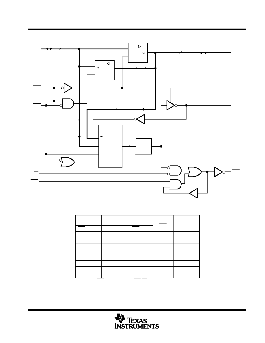
logic diagram (positive logic)
PARITY
ERR
CLR
B1≠B8
A1≠ A8
LE
OEA
OEB
EN
EN
8x
8x
MUX
1
1
G1
1
1
2k
P
8
9
8
8
8
8
Pin numbers shown are for the DB, DW, JT, NT, PW, and W packages.
2≠9
14
1
13
11
23≠16
15
10
ERROR-FLAG FUNCTION TABLE
INPUTS
INTERNAL
TO DEVICE
OUTPUT
PRESTATE
OUTPUT
ERR
FUNCTION
CLR
LE
POINT P
ERRN≠1
ERR
L
L
L
X
L
Pass
L
L
H
X
H
Pass
L
X
L
H
L
X
L
L
Sample
H
H
H
L
H
X
X
H
Clear
H
H
X
L
L
Store
H
H
X
H
H
Store
The state of ERR before changes at CLR, LE, or point P
SN54ABT853, SN74ABT853
8-BIT TO 9-BIT PARITY BUS TRANSCEIVERS
SCBS198F ≠ FEBRUARY 1991 ≠ REVISED OCTOBER 1997
4
POST OFFICE BOX 655303
∑
DALLAS, TEXAS 75265
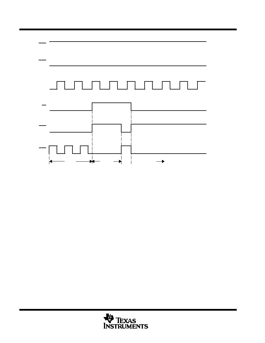
error-flag waveforms
ERR
CLR
LE
OEA
OEB
Bi + PARITY
H
L
H
L
Even
Odd
H
L
H
L
H
L
Pass
Store
Sample
Clear
absolute maximum ratings over operating free-air temperature range (unless otherwise noted)
Supply voltage range, V
CC
≠0.5 V to 7 V
. . . . . . . . . . . . . . . . . . . . . . . . . . . . . . . . . . . . . . . . . . . . . . . . . . . . . . . . . .
Input voltage range, V
I
: Except I/O ports (see Note 1)
≠0.5 V to 7 V
. . . . . . . . . . . . . . . . . . . . . . . . . . . . . . . . . .
Voltage range applied to any output in the high or power-off state, V
O
≠0.5 V to 5.5 V
. . . . . . . . . . . . . . . . . . .
Current into any output in the low state, I
O
: SN54ABT853 96
mA
. . . . . . . . . . . . . . . . . . . . . . . . . . . . . . . . . . . . .
SN74ABT853
128 mA
. . . . . . . . . . . . . . . . . . . . . . . . . . . . . . . . . . . . .
Input clamp current, I
IK
(V
I
< 0)
≠18 mA
. . . . . . . . . . . . . . . . . . . . . . . . . . . . . . . . . . . . . . . . . . . . . . . . . . . . . . . . . . .
Output clamp current, I
OK
(V
O
< 0)
≠50 mA
. . . . . . . . . . . . . . . . . . . . . . . . . . . . . . . . . . . . . . . . . . . . . . . . . . . . . . . .
Package thermal impedance,
JA
(see Note 2): DB package
104
∞
C/W
. . . . . . . . . . . . . . . . . . . . . . . . . . . . . . . . .
DW package
81
∞
C/W
. . . . . . . . . . . . . . . . . . . . . . . . . . . . . . . . .
N package
67
∞
C/W
. . . . . . . . . . . . . . . . . . . . . . . . . . . . . . . . . . .
PW package
120
∞
C/W
. . . . . . . . . . . . . . . . . . . . . . . . . . . . . . . .
Storage temperature range, T
stg
≠65
∞
C to 150
∞
C
. . . . . . . . . . . . . . . . . . . . . . . . . . . . . . . . . . . . . . . . . . . . . . . . . . .
Stresses beyond those listed under "absolute maximum ratings" may cause permanent damage to the device. These are stress ratings only, and
functional operation of the device at these or any other conditions beyond those indicated under "recommended operating conditions" is not
implied. Exposure to absolute-maximum-rated conditions for extended periods may affect device reliability.
NOTES:
1. The input and output negative-voltage ratings may be exceeded if the input and output clamp-current ratings are observed.
2. The package thermal impedance is calculated in accordance with JESD 51, except for through-hole packages, which use a trace
length of zero.

SN54ABT853, SN74ABT853
8-BIT TO 9-BIT PARITY BUS TRANSCEIVERS
SCBS198F ≠ FEBRUARY 1991 ≠ REVISED OCTOBER 1997
5
POST OFFICE BOX 655303
∑
DALLAS, TEXAS 75265
recommended operating conditions (see Note 3)
SN54ABT853
SN74ABT853
UNIT
MIN
MAX
MIN
MAX
UNIT
VCC
Supply voltage
4.5
5.5
4.5
5.5
V
VIH
High-level input voltage
2
2
V
VIL
Low-level input voltage
0.8
0.8
V
VI
Input voltage
0
VCC
0
VCC
V
VOH
High-level output voltage
ERR
5.5
5.5
V
IOH
High-level output current
Except ERR
≠24
≠32
mA
IOL
Low-level output current
48
64
mA
t/
v
Input transition rise or fall rate
Outputs enabled
10
10
ns/V
t/
VCC
Power-up ramp rate
200
200
µ
s/V
TA
Operating free-air temperature
≠55
125
≠40
85
∞
C
NOTE 3: Unused pins (input or I/O) must be held high or low to prevent them from floating.