Document Outline
- IMPORTANT NOTICE
- Contents
- List of Illustrations
- List of Tables
- Introduction
- Features (TVP3010C and TVP 3010M)
- Functional Block Diagram
- Terminal Assignments
- Ordering Information
- Terminal Functions (TVP3010C and TVP3010M)
- Detailed Description
- MPU Interface
- Color Palette
- Writing to Color-Palette RAM
- Reading From Color-Palette RAM
- Palette Page Register
- Read Masking
- Clock Selection and Output-Clock (SCLK, RCLK, and VCLK) Generation
- RCLK, SCLK, VCLK
- Frame-Buffer Clocking: Self-Clocked or Externally Clocked
- Multiplexing Scheme
- Little-Endian and Big-Endian Data Format
- VGA Pass-Through Mode
- Pseudo-Color Mode
- Direct-Color Mode
- True-Color Mode
- Multiplexer Control Registers
- On-Chip Cursor
- Cursor RAM
- Two-Color 64X 64 Cursor
- 64X 64 Cursor Positioning
- Crosshair Cursor
- Dual-Cursor Positioning
- Auxiliary Window, Port Select, and Color-Key Switching
- Windowing Control
- Color-Key Switching Control
- Overscan
- Horizontal Zooming
- Test Functions
- 16-Bit CRC
- Sense-Comparator Output and Test Register
- MUXOUT [SENSE]Output
- Reset
- Power-On Reset
- Software Reset
- Frame-Buffer Interface
- Analog-Output Specifications
- Video Control: Horizontal Sync, Vertical Sync, and Blank
- Split Shift Register Transfer VRAMs
- Control Register Definitions
- Configuration Register
- General Control Register
- Cursor Control Register
- Cursor Position X and Y Registers
- Sprite Origin X and Y Registers
- Window Start X and Y Registers
- Window Stop X and Y Registers
- Cursor Color 0, 1 RGB Registers
- Cursor RAM Address Register
- Cursor RAM Data Register
- Auxiliary-Control Register
- Color-Key Control Register
- Color-Key (Red, Green, Blue, Overlay) Low and High Registers
- Overscan-Color RGB Registers
- CRC LSB and MSB Registers
- CRC Control Register
- Electrical Characteristics
- Absolute Maximum Ratings Over Operating Free-Air Temperature Range (unl\
ess otherwise noted)
- Recommended Operating Conditions
- Electrical Characteristics for TVP3010C Over Recommended Ranges of Suppl\
y Voltage and Operating Free-Air Temperature (Unless Otherwise Noted)\
- Electrical Characteristics for TVP3010M Over Recommended Ranges of Supp\
ly Voltage and Operating Free-Air Temperature (Unless Otherwise Noted)\
- Operating Characteristics (TVP3010C) (see Note 4)
- Operating Characteristics (TVP3010M)
- Timing Requirements (TVP3010C) (see Note 6)
- Timing Requirements (TVP3010M) (see Note 6)
- Switching Characteristics for TVP3010C Over Recommended Ranges of Supply\
Voltage and Operating Free-Air Temperature (see Figures 3-1 to 3-3)
- Switching Characteristics for TVP3010C Over Recommended Ranges of Suppl\
y Voltage and Operating Free-Air Temperature (see Figures 3-1 to 3-3) \
(Continued)
- Switching Characteristics for TVP3010M, Over Recommended Ranges of Suppl\
y Voltage and Operating Free-Air Temperature (see Figures 3-1 to 3-3)
- Timing Diagrams
- Printed Circuit Board Layout Considerations
- PRINTED CIRCUIT BOARD (PCB) Considerations
- Ground Plane
- Power Plane
- Supply Decoupling
- COMP and REF Terminals
- Analog-Output Protection
- RCLK Frequency < VCLK Frequency
- Little-Endian and Big-Endian Data Formats
- Examples: Register Settings
- Mechanical Data
- FN (S-PQCC-J**) PLASTIC QUAD CHIP CARRIER
- GA-GB (S-CPGA-P12 X 12) CERAMIC PIN GRID ARRAY PACKAGE

TVP3010C, TVP3010M
Data Manual
Video Interface Palette
SLAS082A
Printed on Recycled Paper
SLAS082A
October 1997

IMPORTANT NOTICE
Texas Instruments (TI) reserves the right to make changes to its products or to discontinue any
semiconductor product or service without notice, and advises its customers to obtain the latest
version of relevant information to verify, before placing orders, that the information being relied
on is current.
TI warrants performance of its semiconductor products and related software to the specifications
applicable at the time of sale in accordance with TI's standard warranty. Testing and other quality
control techniques are utilized to the extent TI deems necessary to support this warranty.
Specific testing of all parameters of each device is not necessarily performed, except those
mandated by government requirements.
Certain applications using semiconductor products may involve potential risks of death,
personal injury, or severe property or environmental damage ("Critical Applications").
TI SEMICONDUCTOR PRODUCTS ARE NOT DESIGNED, INTENDED, AUTHORIZED, OR
WARRANTED TO BE SUITABLE FOR USE IN LIFE-SUPPORT APPLICATIONS, DEVICES
OR SYSTEMS OR OTHER CRITICAL APPLICATIONS.
Inclusion of TI products in such applications is understood to be fully at the risk of the customer.
Use of TI products in such applications requires the written approval of an appropriate TI officer.
Questions concerning potential risk applications should be directed to TI through a local SC
sales office.
In order to minimize risks associated with the customer's applications, adequate design and
operating safeguards should be provided by the customer to minimize inherent or procedural
hazards.
TI assumes no liability for applications assistance, customer product design, software
performance, or infringement of patents or services described herein. Nor does TI warrant or
represent that any license, either express or implied, is granted under any patent right, copyright,
mask work right, or other intellectual property right of TI covering or relating to any combination,
machine, or process in which such semiconductor products or services might be or are used.
Copyright
�
1997, Texas Instruments Incorporated

iii
Contents
Section
Title
Page
1
Introduction
1�1
. . . . . . . . . . . . . . . . . . . . . . . . . . . . . . . . . . . . . . . . . . . . . . . . . . . . . . . . . . . . . . .
1.1
Features (TVP3010C and TVP3010M)
1�3
. . . . . . . . . . . . . . . . . . . . . . . . . . . . . . . . . . . .
1.2
Functional Block Diagram
1�4
. . . . . . . . . . . . . . . . . . . . . . . . . . . . . . . . . . . . . . . . . . . . . . .
1.3
Terminal Assignments
1�5
. . . . . . . . . . . . . . . . . . . . . . . . . . . . . . . . . . . . . . . . . . . . . . . . . .
1.4
Ordering Information
1�7
. . . . . . . . . . . . . . . . . . . . . . . . . . . . . . . . . . . . . . . . . . . . . . . . . . .
1.5
Terminal Functions (TVP3010C and TVP3010M)
1�7
. . . . . . . . . . . . . . . . . . . . . . . . . . .
2
Detailed Description
2�1
. . . . . . . . . . . . . . . . . . . . . . . . . . . . . . . . . . . . . . . . . . . . . . . . . . . . . . .
2.1
MPU Interface
2�1
. . . . . . . . . . . . . . . . . . . . . . . . . . . . . . . . . . . . . . . . . . . . . . . . . . . . . . . . .
2.2
Color Palette
2�4
. . . . . . . . . . . . . . . . . . . . . . . . . . . . . . . . . . . . . . . . . . . . . . . . . . . . . . . . . .
2.2.1
Writing to Color-Palette RAM
2�4
. . . . . . . . . . . . . . . . . . . . . . . . . . . . . . . . . . . .
2.2.2
Reading From Color-Palette RAM
2�4
. . . . . . . . . . . . . . . . . . . . . . . . . . . . . . .
2.2.3
Palette Page Register
2�4
. . . . . . . . . . . . . . . . . . . . . . . . . . . . . . . . . . . . . . . . . .
2.2.4
Read Masking
2�5
. . . . . . . . . . . . . . . . . . . . . . . . . . . . . . . . . . . . . . . . . . . . . . . .
2.3
Clock Selection and Output-Clock (SCLK, RCLK, and VCLK) Generation
2�5
. . . . .
2.3.1
RCLK, SCLK, VCLK
2�5
. . . . . . . . . . . . . . . . . . . . . . . . . . . . . . . . . . . . . . . . . . .
2.3.2
Frame-Buffer Clocking: Self-Clocked or Externally Clocked
2�8
. . . . . . . . .
2.4
Multiplexing Scheme
2�12
. . . . . . . . . . . . . . . . . . . . . . . . . . . . . . . . . . . . . . . . . . . . . . . . . .
2.4.1
Little-Endian and Big-Endian Data Format
2�12
. . . . . . . . . . . . . . . . . . . . . . .
2.4.2
VGA Pass-Through Mode
2�13
. . . . . . . . . . . . . . . . . . . . . . . . . . . . . . . . . . . . .
2.4.3
Pseudo-Color Mode
2�13
. . . . . . . . . . . . . . . . . . . . . . . . . . . . . . . . . . . . . . . . . .
2.4.4
Direct-Color Mode
2�13
. . . . . . . . . . . . . . . . . . . . . . . . . . . . . . . . . . . . . . . . . . . .
2.4.5
True-Color Mode
2�14
. . . . . . . . . . . . . . . . . . . . . . . . . . . . . . . . . . . . . . . . . . . . .
2.4.6
Multiplex Control Registers
2�22
. . . . . . . . . . . . . . . . . . . . . . . . . . . . . . . . . . . .
2.5
On-Chip Cursor
2�23
. . . . . . . . . . . . . . . . . . . . . . . . . . . . . . . . . . . . . . . . . . . . . . . . . . . . . . .
2.5.1
Cursor RAM
2�23
. . . . . . . . . . . . . . . . . . . . . . . . . . . . . . . . . . . . . . . . . . . . . . . . .
2.5.2
Two-Color 64
�
64 Cursor
2�24
. . . . . . . . . . . . . . . . . . . . . . . . . . . . . . . . . . . . .
2.5.3
64
�
64 Cursor Positioning
2�24
. . . . . . . . . . . . . . . . . . . . . . . . . . . . . . . . . . . . .
2.5.4
Crosshair Cursor
2�25
. . . . . . . . . . . . . . . . . . . . . . . . . . . . . . . . . . . . . . . . . . . . .
2.5.5
Dual-Cursor Positioning
2�26
. . . . . . . . . . . . . . . . . . . . . . . . . . . . . . . . . . . . . . .
2.6
Auxiliary Window, Port Select, and Color-Key Switching
2�27
. . . . . . . . . . . . . . . . . . . .
2.6.1
Windowing Control
2�28
. . . . . . . . . . . . . . . . . . . . . . . . . . . . . . . . . . . . . . . . . . .
2.6.2
Color-Key-Switching Control
2�30
. . . . . . . . . . . . . . . . . . . . . . . . . . . . . . . . . . .
2.7
Overscan
2�31
. . . . . . . . . . . . . . . . . . . . . . . . . . . . . . . . . . . . . . . . . . . . . . . . . . . . . . . . . . . .
2.8
Horizontal Zooming
2�32
. . . . . . . . . . . . . . . . . . . . . . . . . . . . . . . . . . . . . . . . . . . . . . . . . . .
2.9
Test Functions
2�33
. . . . . . . . . . . . . . . . . . . . . . . . . . . . . . . . . . . . . . . . . . . . . . . . . . . . . . . .
2.9.1
16-Bit CRC
2�33
. . . . . . . . . . . . . . . . . . . . . . . . . . . . . . . . . . . . . . . . . . . . . . . . . .
2.9.2
Sense-Comparator Output and Test Register
2�33
. . . . . . . . . . . . . . . . . . . . .
2.9.3
Identification Code (ID) Register
2�34
. . . . . . . . . . . . . . . . . . . . . . . . . . . . . . . .
2.10 MUXOUT [SENSE]Output
2�34
. . . . . . . . . . . . . . . . . . . . . . . . . . . . . . . . . . . . . . . . . . . . .

iv
Section
Title
Page
2.11 Reset
2�34
. . . . . . . . . . . . . . . . . . . . . . . . . . . . . . . . . . . . . . . . . . . . . . . . . . . . . . . . . . . . . . .
2.11.1
Power-On Reset
2�34
. . . . . . . . . . . . . . . . . . . . . . . . . . . . . . . . . . . . . . . . . . . . .
2.11.2
Software Reset
2�34
. . . . . . . . . . . . . . . . . . . . . . . . . . . . . . . . . . . . . . . . . . . . . . .
2.12 Frame-Buffer Interface
2�35
. . . . . . . . . . . . . . . . . . . . . . . . . . . . . . . . . . . . . . . . . . . . . . . .
2.13 Analog-Output Specifications
2�35
. . . . . . . . . . . . . . . . . . . . . . . . . . . . . . . . . . . . . . . . . . .
2.14 Video Control: Horizontal Sync, Vertical Sync, and Blank
2�37
. . . . . . . . . . . . . . . . . . .
2.15 Split Shift Register Transfer VRAMs
2�37
. . . . . . . . . . . . . . . . . . . . . . . . . . . . . . . . . . . . .
2.16 Control Register Definitions
2�38
. . . . . . . . . . . . . . . . . . . . . . . . . . . . . . . . . . . . . . . . . . . .
2.16.1
Configuration Register
2�38
. . . . . . . . . . . . . . . . . . . . . . . . . . . . . . . . . . . . . . . .
2.16.2
General Control Register
2�39
. . . . . . . . . . . . . . . . . . . . . . . . . . . . . . . . . . . . . .
2.16.3
Cursor Control Register
2�40
. . . . . . . . . . . . . . . . . . . . . . . . . . . . . . . . . . . . . . .
2.16.4
Cursor Position X and Y Registers
2�41
. . . . . . . . . . . . . . . . . . . . . . . . . . . . . .
2.16.5
Sprite Origin X and Y Registers
2�42
. . . . . . . . . . . . . . . . . . . . . . . . . . . . . . . .
2.16.6
Window Start X and Y Registers
2�43
. . . . . . . . . . . . . . . . . . . . . . . . . . . . . . . .
2.16.7
Window Stop X and Y Registers
2�44
. . . . . . . . . . . . . . . . . . . . . . . . . . . . . . . .
2.16.8
Cursor Color 0, 1 RGB Registers
2�45
. . . . . . . . . . . . . . . . . . . . . . . . . . . . . . .
2.16.9
Cursor-RAM Address Register
2�46
. . . . . . . . . . . . . . . . . . . . . . . . . . . . . . . . .
2.16.10 Cursor RAM Data Register
2�46
. . . . . . . . . . . . . . . . . . . . . . . . . . . . . . . . . . . .
2.16.11
AuxiliaryControl Register
2�47
. . . . . . . . . . . . . . . . . . . . . . . . . . . . . . . . . . . . . .
2.16.12 Color-Key-Control Register
2�48
. . . . . . . . . . . . . . . . . . . . . . . . . . . . . . . . . . . .
2.16.13 Color-Key (Red, Green, Blue, Overlay) Low and High Registers
2�49
. . . .
2.16.14 Overscan Color RGB Registers
2�50
. . . . . . . . . . . . . . . . . . . . . . . . . . . . . . . .
2.16.15 CRC LSB and MSB Registers
2�51
. . . . . . . . . . . . . . . . . . . . . . . . . . . . . . . . . .
2.16.16 CRC Control Register
2�51
. . . . . . . . . . . . . . . . . . . . . . . . . . . . . . . . . . . . . . . . .
3
Electrical Characteristics
3�1
. . . . . . . . . . . . . . . . . . . . . . . . . . . . . . . . . . . . . . . . . . . . . . . . . .
3.1
Absolute Maximum Ratings Over Operating Free-Air Temperature Range
3�1
. . . .
3.2
Recommended Operating Conditions
3�1
. . . . . . . . . . . . . . . . . . . . . . . . . . . . . . . . . . . . .
3.3
Electrical Characteristics for TVP3010C Over Recommended Ranges of
Supply Voltage and Operating Free-Air Temperature
3�2
. . . . . . . . . . . . . . . . . . . . . . .
3.4
Electrical Characteristics for TVP3010M Over Recommended Ranges of
Supply Voltage and Operating Free-Air Temperature
3�3
. . . . . . . . . . . . . . . . . . . . . . .
3.5
Operating Characteristics (TVP3010C)
3�4
. . . . . . . . . . . . . . . . . . . . . . . . . . . . . . . . . . .
3.6
Operating Characteristics (TVP3010M)
3�5
. . . . . . . . . . . . . . . . . . . . . . . . . . . . . . . . . . .
3.7
Timing Requirements (TVP3010C)
3�6
. . . . . . . . . . . . . . . . . . . . . . . . . . . . . . . . . . . . . . .
3.8
Timing Requirements (TVP3010M)
3�7
. . . . . . . . . . . . . . . . . . . . . . . . . . . . . . . . . . . . . . .
3.9
Switching Characteristics for TVP3010C Over Recommended Ranges of
Supply Voltage and Operating Free-Air Temperature
3�8
. . . . . . . . . . . . . . . . . . . . . . .
3.10 Switching Characteristics for TVP3010M Over Recommended Ranges of
Supply Voltage and Operating Free-Air Temperature
3�10
. . . . . . . . . . . . . . . . . . . . . .
3.11 Timing Diagrams
3�11
. . . . . . . . . . . . . . . . . . . . . . . . . . . . . . . . . . . . . . . . . . . . . . . . . . . . . .

v
Section
Title
Page
Appendix A
Printed Circuit Board Layout Considerations
A�1
. . . . . . . . . . . . . . . . . . . . .
Appendix B
RCLK Frequency < VCLK Frequency
B�1
. . . . . . . . . . . . . . . . . . . . . . . . . . . . .
Appendix C
Little-Endian and Big-Endian Data Formats
C�1
. . . . . . . . . . . . . . . . . . . . . . .
Appendix D
Examples: Register Settings
D�1
. . . . . . . . . . . . . . . . . . . . . . . . . . . . . . . . . . . . .
Appendix E
Mechanical Data
E�1
. . . . . . . . . . . . . . . . . . . . . . . . . . . . . . . . . . . . . . . . . . . . . . . .
List of Illustrations
Figure
Title
Page
2�1
Dot Clock / VCLK/ RCLK / SCLK Relationship
2�7
. . . . . . . . . . . . . . . . . . . . . . . . . . . . . . . .
2�2
SCLK/ VCLK Control Timing
(SSRT Disabled, RCLK / SCLK Frequency = VCLK Frequency)
2�8
. . . . . . . . . . . . . . . .
2�3
SCLK/VCLK Control Timing
(SSRT Enabled, RCLK/SCLK Frequency = VCLK Frequency)
2�9
. . . . . . . . . . . . . . . .
2�4
SCLK/VCLK Control Timing
(SSRT Disabled, RCLK/SCLK Frequency = 4 x VCLK Frequency)
2�10
. . . . . . . . . . . .
2�5
SCLK/VCLK Control Timing
(SSRT Enabled, RCLK/SCLK Frequency = 4 x VCLK Frequency)
2�10
. . . . . . . . . . . .
2�6
CursorRAM Organization
2�24
. . . . . . . . . . . . . . . . . . . . . . . . . . . . . . . . . . . . . . . . . . . . . . .
2�7
Common Sprite-Origin Settings
2�25
. . . . . . . . . . . . . . . . . . . . . . . . . . . . . . . . . . . . . . . . . .
2�8
Dual-Cursor Positioning
2�26
. . . . . . . . . . . . . . . . . . . . . . . . . . . . . . . . . . . . . . . . . . . . . . . . .
2�9
One Possible Custom-Cursor Creation
2�26
. . . . . . . . . . . . . . . . . . . . . . . . . . . . . . . . . . . .
2�10
VGA in the Auxiliary Window
2�29
. . . . . . . . . . . . . . . . . . . . . . . . . . . . . . . . . . . . . . . . . . . .
2�11
Multiple VGA Windows Using Port Select (PSEL)
2�30
. . . . . . . . . . . . . . . . . . . . . . . . . .
2�12
Overscan
2�32
. . . . . . . . . . . . . . . . . . . . . . . . . . . . . . . . . . . . . . . . . . . . . . . . . . . . . . . . . . . . .
2�13
Equivalent Circuit of the Current Output (IOG)
2�35
. . . . . . . . . . . . . . . . . . . . . . . . . . . . .
2�14
Composite Video Output (With 0 IRE, 8-Bit Output)
2�36
. . . . . . . . . . . . . . . . . . . . . . . . .
2�15
Composite Video Output (With 7.5 IRE, 8-Bit Output)
2�36
. . . . . . . . . . . . . . . . . . . . . . .
2�16
Split Shift Register Transfer Timing
2�37
. . . . . . . . . . . . . . . . . . . . . . . . . . . . . . . . . . . . . . .
3�1
MPU Interface Timing
3�11
. . . . . . . . . . . . . . . . . . . . . . . . . . . . . . . . . . . . . . . . . . . . . . . . . . .
3�2
Video Input /Output Timing
3�12
. . . . . . . . . . . . . . . . . . . . . . . . . . . . . . . . . . . . . . . . . . . . . .
3�3
SFLAG Timing (When SSRT Function is Enabled)
3�13
. . . . . . . . . . . . . . . . . . . . . . . . . .

vi
List of Tables
Table
Title
Page
2�1
Direct Register Map
2�1
. . . . . . . . . . . . . . . . . . . . . . . . . . . . . . . . . . . . . . . . . . . . . . . . . . . . .
2�2
Indirect Register Map (Extended Registers)
2�2
. . . . . . . . . . . . . . . . . . . . . . . . . . . . . . . .
2�3
Allocation of Palette-Page Register Bits
2�5
. . . . . . . . . . . . . . . . . . . . . . . . . . . . . . . . . . . .
2�4
Input-Clock-Selection Register
2�7
. . . . . . . . . . . . . . . . . . . . . . . . . . . . . . . . . . . . . . . . . . . .
2�5
Output-Clock-Selection Register Format
2�6
. . . . . . . . . . . . . . . . . . . . . . . . . . . . . . . . . . .
2�6
Multiplex Mode and Bus-Width Selection
2�15
. . . . . . . . . . . . . . . . . . . . . . . . . . . . . . . . . .
2�7
Pseudo-Color Mode Pixel-Latching Sequence
2�18
. . . . . . . . . . . . . . . . . . . . . . . . . . . . .
2�8
Direct-Color Mode Pixel-Latching Sequence (Little Endian)
2�19
. . . . . . . . . . . . . . . . . .
2�9
Direct-Color Mode Pixel-Latching Sequence (Big Endian)
2�20
. . . . . . . . . . . . . . . . . . .
2�10
True-Color Mode Pixel-Latching Sequence (Little Endian)
2�21
. . . . . . . . . . . . . . . . . . .
2�11
True-Color Mode Pixel-Latching Sequence (Big Endian)
2�22
. . . . . . . . . . . . . . . . . . . .
2�12
Two-Color 64
�
64 Cursor-RAM Selection
2�24
. . . . . . . . . . . . . . . . . . . . . . . . . . . . . . . . .
2�13
Crosshair-Cursor Color Selection
2�25
. . . . . . . . . . . . . . . . . . . . . . . . . . . . . . . . . . . . . . . .
2�14
Cursor-Intersection Truth Table
2�27
. . . . . . . . . . . . . . . . . . . . . . . . . . . . . . . . . . . . . . . . . .
2�15
Windowing Control
2�28
. . . . . . . . . . . . . . . . . . . . . . . . . . . . . . . . . . . . . . . . . . . . . . . . . . . . .
2�16
Zoom Control
2�32
. . . . . . . . . . . . . . . . . . . . . . . . . . . . . . . . . . . . . . . . . . . . . . . . . . . . . . . . . .
2�17
Sense-Test Register
2�34
. . . . . . . . . . . . . . . . . . . . . . . . . . . . . . . . . . . . . . . . . . . . . . . . . . . .
2�18
K1 and K2 Values Defined
2�36
. . . . . . . . . . . . . . . . . . . . . . . . . . . . . . . . . . . . . . . . . . . . . .
2�19
Configuration Register
2�38
. . . . . . . . . . . . . . . . . . . . . . . . . . . . . . . . . . . . . . . . . . . . . . . . . .
2�20
General Control Register
2�39
. . . . . . . . . . . . . . . . . . . . . . . . . . . . . . . . . . . . . . . . . . . . . . . .
2�21
Cursor Control Register
2�40
. . . . . . . . . . . . . . . . . . . . . . . . . . . . . . . . . . . . . . . . . . . . . . . . .
2�22
Cursor Position X (LSB) and X (MSB)
2�41
. . . . . . . . . . . . . . . . . . . . . . . . . . . . . . . . . . . . .
2�23
Sprite Origin X and Y Registers
2�42
. . . . . . . . . . . . . . . . . . . . . . . . . . . . . . . . . . . . . . . . . .
2�24
Window Start X and Y Registers
2�43
. . . . . . . . . . . . . . . . . . . . . . . . . . . . . . . . . . . . . . . . .
2�25
Window Stop X and Y Registers
2�44
. . . . . . . . . . . . . . . . . . . . . . . . . . . . . . . . . . . . . . . . .
2�26
Cursor-Color RGB Registers
2�45
. . . . . . . . . . . . . . . . . . . . . . . . . . . . . . . . . . . . . . . . . . . .
2�27
Cursor RAM Address Register
2�46
. . . . . . . . . . . . . . . . . . . . . . . . . . . . . . . . . . . . . . . . . . .
2�28
Cursor RAM Data Register
2�46
. . . . . . . . . . . . . . . . . . . . . . . . . . . . . . . . . . . . . . . . . . . . . .
2�29
Auxiliary-Control Register
2�47
. . . . . . . . . . . . . . . . . . . . . . . . . . . . . . . . . . . . . . . . . . . . . . .
2�30
Color-Key Control Register
2�48
. . . . . . . . . . . . . . . . . . . . . . . . . . . . . . . . . . . . . . . . . . . . . .
2�31
Color-Key Low and High Registers
2�49
. . . . . . . . . . . . . . . . . . . . . . . . . . . . . . . . . . . . . . .
2�32
Overscan-Color RGB Register
2�50
. . . . . . . . . . . . . . . . . . . . . . . . . . . . . . . . . . . . . . . . . . .
2�33
CRC MSB and LSB Registers
2�51
. . . . . . . . . . . . . . . . . . . . . . . . . . . . . . . . . . . . . . . . . . .
2�34
CRC Control Register Format
2�51
. . . . . . . . . . . . . . . . . . . . . . . . . . . . . . . . . . . . . . . . . . . .

1�1
1 Introduction
The TVP3010C and the TVP3010M palettes are commercial and military versions, respectively, of an
advanced Video Interface Palette (VIP) from Texas Instruments implemented in the EPIC
TM
0.8-micron
CMOS process. Differences between the two versions are outlined in separate tables. In both versions,
maximum flexibility is provided by the pixel multiplexing scheme. The scheme accommodates 64-, 32-, 16-,
8-, and 4-bit pixel buses without any circuit modification. This enables the system to be easily reconfigured
for varying amounts of available video RAM. The device supports selection of little- or big-endian data format
for the pixel-bus/frame-buffer interface. Data can be split into 1, 2, 4, or 8 bit-planes for pseudo-color mode
or split into 12-, 16- or 24-bit true-color and direct-color modes. For the 24-bit direct-color modes, an 8-bit
overlay plane is available. The 16-bit direct-color and true-color modes can be configured to IBM XGA
�
(5, 6, 5), TARGA
�
(5, 5, 5, 1), or (6, 6, 4) as another existing format. An additional 12-bit mode (4, 4, 4, 4)
is supported with 4 bits for each color and overlay. An on-chip, IBM XGA-compatible hardware cursor is
incorporated so that further increases in graphics-system performance are possible. Both devices are
software compatible with the INMOS
TM
IMSG176/8 and Brooktree
TM
Bt476/8 color palettes.
An internal-frequency doubler is incorporated, allowing convenient and cost-effective clock-source
alternatives to be utilized. An auxiliary windowing function and a pixel-port select function are provided so
that overlay or VGA graphics can be displayed on top of direct color inside or outside a specified auxiliary
window. Color-keyed switching of direct color and overlay is also supported.
Clocking is provided through one of five TTL inputs, CLK0 � CLK4, and is software selectable. Additionally,
CLK1/CLK2 and CLK3/CLK4 can be selected as differential ECL clock sources. The video, shift-clock, and
reference-clock outputs provide a software-selected divide ratio of the chosen clock input. The reference
clock can optionally be provided as an output on CLK3, and a data-latch clock can optionally be input on
CLK4.
The TVP3010C and the TVP3010M have three 256
8 color look-up tables with triple 8-bit video
digital-to-analog converters (DACs) capable of directly driving a doubly-terminated 75-
line. The lookup
tables are designed with a dual-ported RAM architecture that enables ultra-high speed operation. Sync
generation is incorporated on the green output channel. Horizontal sync and vertical sync are fed through
the device and optionally inverted to indicate screen resolution to the monitor. A palette-page register
provides the additional bits of palette address when 1, 2, or 4 bit-planes are used. This allows the screen
colors to be changed with only one microprocessor-interface unit (MPU) write cycle.
Each device features a separate VGA bus that allows data from the feature connector of most
VGA-supported personal computers to be fed directly into the palette without the need for external data
multiplexing. This allows a replacement graphics board to remain downwards compatible by utilizing the
existing graphics circuitry often located on the motherboard.
Both the TVP3010 VIP and the TVP3010M VIP are highly system integrated. Either device can be
connected to the serial port of a VRAM device without external buffer logic and each device can be
connected to many graphics engines directly. The split shift register transfer function, which is supported
by VRAM, is also supported by the TVP3010C and TVP3010M.
The system-integration concept is carried to manufacturing testing and field diagnosis levels. To support
these testing and diagnostic levels, several highly-integrated test functions have been designed to enable
simplified testing of the palette, the graphics board, and the graphics system.
EPIC is a trademark of Texas Instruments Incorporated.
XGA is a registered trademark of International Business Machines Corporation.
TARGA is a registered trademark of Truevision Incorporated.
INMOS is a trademark of INMOS International Limited.
Brooktree is a trademark of Brooktree Corporation.

1�2
The TVP3010C and TVP3010M are 32-bit devices and both are pin compatible with the TLC3407X VIP,
allowing convenient performance upgrades when using devices in the TI Video Interface Palette family.
NOTE:
The TVP3010C and TVP3010M include circuits that are patented as well as circuit
designs that have patents pending.

1�3
1.1
Features (TVP3010C and TVP 3010M)
�
Second-Generation Video Interface Palette
�
Supports System Resolutions of:
�
1600
�
1280
�
1, 2, 4, 8, 16 Bits/Pixel @ 60-Hz Refresh Rate
�
1280
�
1024
�
1, 2, 4, 8, 16 Bits/Pixel @ 60-Hz and 72-Hz Refresh Rate
�
1024
�
768
�
1, 2, 4, 8, 16, 24 Bits/Pixel @ 60-Hz and 72-Hz Refresh Rate
�
And Lower Resolutions
�
Direct-Color Modes:
�
24-Bit/Pixel With 8-Bit Overlay
�
16-Bit/Pixel (5, 6, 5) XGA Configuration
�
16-Bit/Pixel (6, 6, 4) Configuration
�
15-Bit/Pixel With 1-Bit Overlay (5, 5, 5, 1) TARGA Configuration
�
12-Bit/Pixel With 4-Bit Overlay (4, 4, 4, 4)
�
True-Color Modes:
�
24-Bit/Pixel With Gamma Correction
�
16-Bit/Pixel (5, 6, 5) XGA Configuration With Gamma Correction
�
16-Bit/Pixel (6, 6, 4) Configuration With Gamma Correction
�
15-Bit/Pixel (5, 5, 5) TARGA Configuration With Gamma Correction
�
12-Bit/Pixel (4, 4, 4) With Gamma Correction
�
RCLK /SCLK /LCLK Data Latching Mechanism to Allow Flexible Control of VRAM Timing
�
Direct Interfacing to Video RAM
�
Support for Split Shift Register Transfers
�
Supports 64-Bit-Wide Pixel Bus
�
On-Chip Hardware Cursor:
�
64
�
64
�
2 Cursor (XGA Functionally Compatible)
�
Full-Window Crosshair
�
Dual-Cursor Mode
�
85-,110-,135-, and 170-MHz Versions
�
Supports Overscan for Creation of Custom Screen Borders
�
Versatile Pixel Bus Interface to Support Little- and Big-Endian Data Formats
�
Windowed-Overlay and VGA Capability
�
Color-Keyed Switching of Direct Color and Overlay
�
On-Chip Clock Selection
�
Internal Frequency Doubler
�
Triple 8-Bit D/A Converters
�
Analog Output Comparators
�
Triple 256
�
8 Color-Palette RAMs
�
RS-343A Compatible Outputs
�
Direct VGA Pass-Through Capability
�
Palette-Page Register
�
Horizontal Zooming Capability
�
Software Downward Compatible With IMSG176/8 and Bt476/8
�
Directly to Graphics Processors
�
EPIC 0.8-
�
m CMOS Process
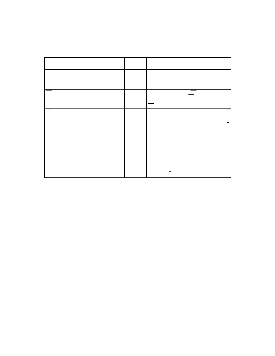
1�4
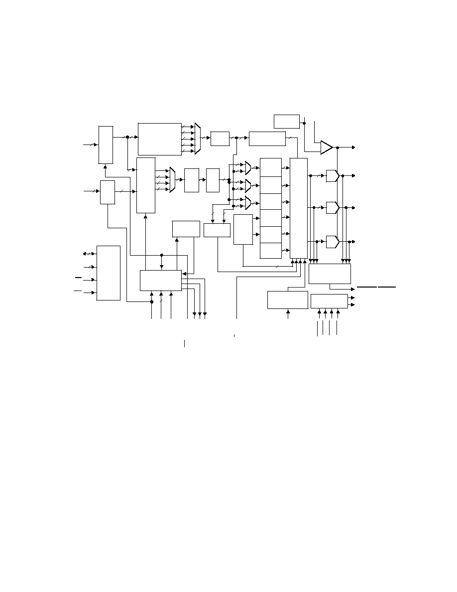
1.2
Functional Block Diagram
The following functional block diagram applies to both the TVP3010C and TVP3010M.
8
12
Input
Latch
8 � 8 � 8
6 � 6 � 4
5 � 6 � 5
5 � 5 � 5
4 � 4 � 4
True-Color
Multiplexer
32 32
24
16
16
15
32
Stuffing
Logic
12 - 24
24 24
Direct-Color
Pipeline Delay
24
Input
Latch
Pseudo-
Color
MUX
1:1
2:1
4:1
8:1
16:1
32:1
2
4
Read
Mask
8
Page
Reg
8
8
8
8
8
8
8
8
256
�
8
Red
RAM
8
8
8
256
�
8
Green
RAM
256
�
8
Blue
RAM
1
�
24
Cursor
Color 0
1
�
24
Cursor
Color 1
1
�
24
Overscan
64
�
64
Cursor
RAM
and
Control
8
8
8
24
24
24
Output
MUX
DAC
8
8
8
DAC
DAC
Vref
1.235 V
REF
FS ADJUST
COMP
IOR
IOG
IOB
Test Function
and
Sense Comparator
Video-Signal
Control
MUXOUT [SENSE]
HSYNCOUT
VSYNCOUT
Auxiliary Window
and
Port Select
2
Clock Select
and
Control
Color-Key
Switch
Frequency
Doubler
2
32
8
8
MPU
Registers
and
Control
Logic
8
3
P(0 � 31)
VGA(0 � 7)
D(0 � 7)
RS(0 � 2)
RD
WR
VGABL
SYSBL
VSYNC
HSYNC
RS3 [PSEL]
8/6 [OVS]
VCLK
SCLK
CLK3 [RCLK]
CLK3 [LCLK]
SFLAG
CLK1/CLK2
CLK0
8
24
1�5
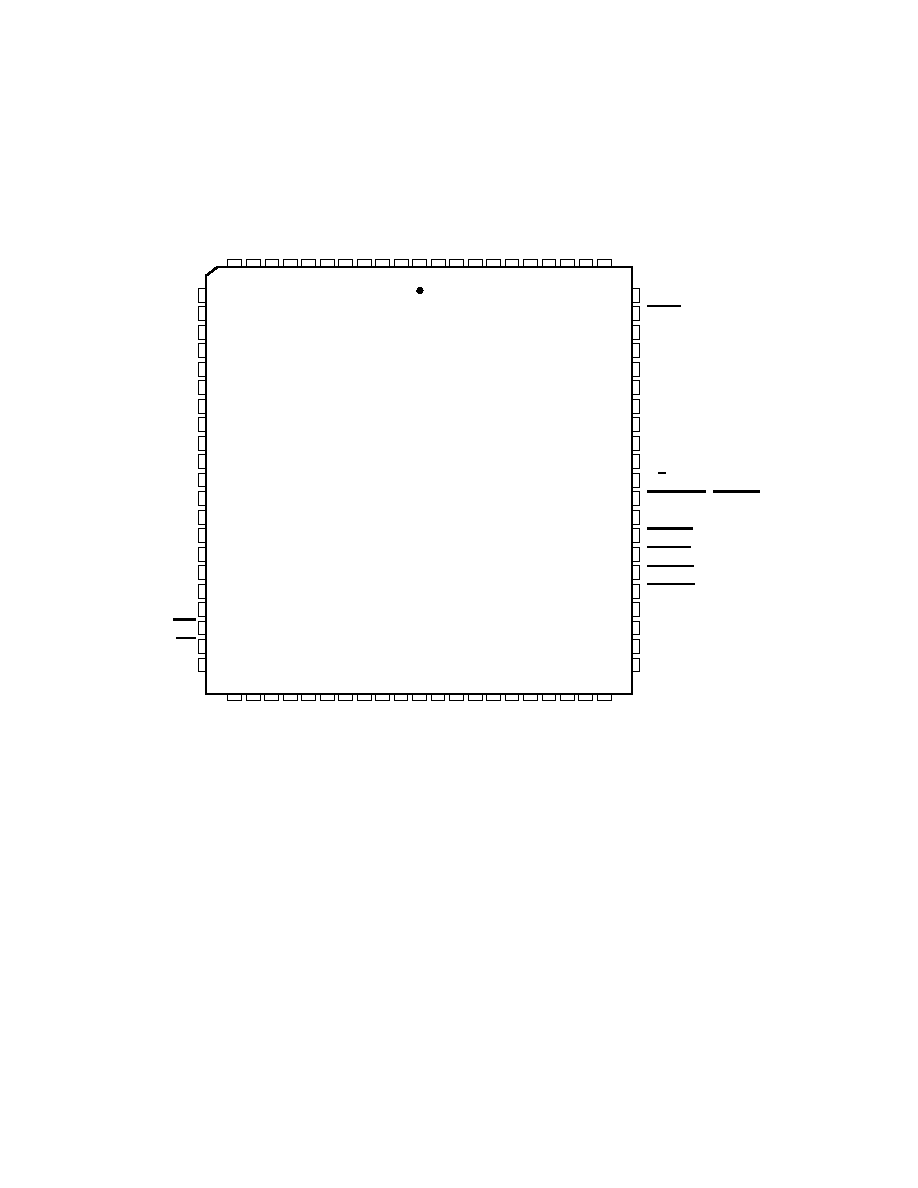
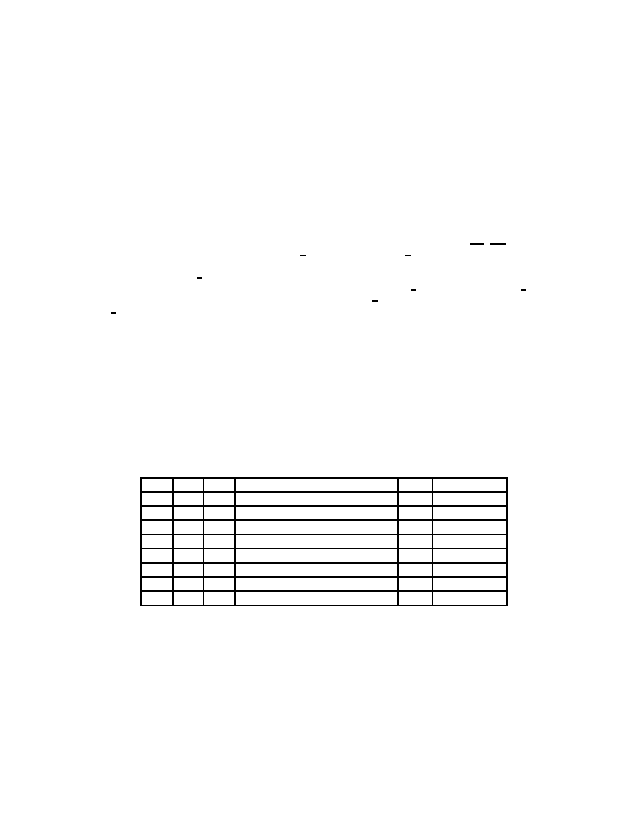
1.3
Terminal Assignments
34 35
CLK3[RCLK]
CLK3[LCLK]
VGA7
VGA6
VGA5
VGA4
VGA3
VGA2
VGA1
VGA0
8/6[OVS]
MUXOUT [SENSE]
SFLAG
VGABL
SYSBL
VSYNC
HSYNC
AV
DD
GND
AV
DD
GND
74
73
72
71
70
69
68
67
66
65
64
63
62
61
60
59
58
57
56
55
54
36
12
13
14
15
16
17
18
19
20
21
22
23
24
25
26
27
28
29
30
31
32
P17
P16
P15
P14
P13
P12
P11
P10
P9
P8
P7
P6
P5
P4
P3
P2
P1
P0
WR
RD
RS0
37 38 39 40
P28
10 9
8
7
6
11
5
P20
P21
P22
P23
P24
P25
P26
D7
RS3[PSEL]
D0
D1
D2
D3
D4
D5
3
2
1
4
41 42 43 44 45
84 83
33
RS1
P30
82 81 80 79
46 47 48 49
HSYNCOUT
VSYNCOUT
IOR
IOG
P31
GND
SCLK
P18
IOB
FS ADJUST
50 51 52 53
VCLK
CLK0
CLK2
78 77 76 75
P19
P27
P29
DV
DD
CLK1
COMP
DV
DD
GND
D6
RS2
REF
84-PIN PLCC PACKAGE

1�6
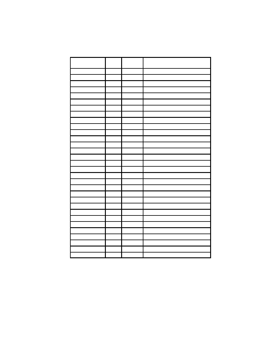
1.3
Terminal Assignments (continued)
RS0
D0
D1
D3
D5
D7
HSYNC-
OUT
AVDD
IOR
IOB
REF
WR
RS2
RS3
[PSEL]
D2
D4
D6
IOG
COMP
P0
RD
RS1
HSYNC
P2
P1
VSYNC
SYSBL
P4
P3
SFLAG
8/6
[OVS]
MUXOUT
[SENSE]
P6
P5
P8
P7
VGA1
VGA0
P9
P10
VGA3
VGA2
P11
P12
P17
VGA5
VGA4
P13
P15
P19
CLK3
[LCLK]
VGA6
CLK2
P14
P16
P22
P24
P27
P29
P31
GND
CLK0
CLK1
VGA7
P21
P18
P20
P23
P25
P26
P28
P30
AVDD
SCLK
VCLK
CLK3
[RCLK]
C
12
11
10
9
8
7
6
5
4
3
2
1
A
B
D
E
F
G
H
J
K
L
M
(ESD symbol or alignment
dot on top)
84-PIN GA PACKAGE (TOP VIEW)
VSYNC-
OUT
FS
ADJUST
GND
AVDD
DVDD
GND
GND
VGABL
1�7
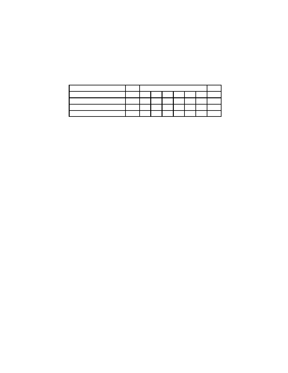
1.4
Ordering Information
TVP3010
XXX � X � XX
Pixel Clock Frequency Indicator
�85:
85-MHz pixel clock
110-MHz pixel clock
135-MHz pixel cock
170-MHz pixel clock
�110:
�135:
�170:
Military Extension M
Package
Must contain two Letters:
FN: square plastic J-leaded chip carrier
GA: 84-pin (12 x 12) ceramic pin-grid array
Must contain three letters:
Commercial Extension C
1.5
Terminal Functions (TVP3010C and TVP3010M)
TERMINAL
I/O
DESCRIPTION
NAME
NO. (FN)
NO. (GA)
I/O
DESCRIPTION
AVDD
55, 57
J1, L11, G12
Analog power. All AVDD terminals must be connected.
CLK0
77
K2
I
(TTL
compatible)
Dot clock 0 input. CLK0 can be selected to drive the dot
clock at frequencies up to 140 MHz. When VGA mode is
active, the default clock source is CLK0. The maximum
frequency in VGA mode is 85 MHz.
CLK1, CLK2
75, 76
L2, K3
I
(TTL /ECL
compatible)
Dual-mode dot clock input. These inputs are essentially
ECL-compatible inputs, but two TTL clocks may be used
on the CLK1 and CLK2 if so selected in the input clock
select register. These inputs may be selected as the dot
clock up to the device limit while in the ECL mode or up to
140 MHz in the TTL mode.
CLK3[RCLK]
74
M1
I/O
Dot clock 3 TTL input or reference clock output. When
configured as CLK3, this terminal is similar to CLK0 and
can be selected to drive the dot clock at frequencies up to
140 MHz. When configured as RCLK, this terminal outputs
the reference clock signal, which is similar to the SCLK
signal but not gated off during blanking. This signal can be
used for pixel-port timing reference or other system
synchronization. The terminal defaults to CLK3 after reset.
CLK3[LCLK]
73
L3
I
Dot clock 4 TTL input or pixel-port latch clock. CLK3[LCLK]
can be configured to drive dot clock frequencies up to 140
MHz, or it can be configured as a latch-clock input to latch
pixel-port input data. It defaults to CLK4 after reset, and
LCLK is internally connected to RCLK to latch pixel-port
data.
COMP
52
K11
I
Compensation. COMP provides compensation for the
internal reference amplifier. A 0.1-
�
F ceramic capacitor is
required between COMP and AVDD. The COMP capacitor
must be as close to the device as possible to avoid noise
pick up.
NOTE 1:
All unused inputs should be tied to a logic level and not be allowed to float.
1�8
1.5
Terminal Functions (TVP3010C and TVP3010M) Continued
TERMINAL
I/O
DESCRIPTION
NAME
NO. (FN)
NO. (GA)
I/O
DESCRIPTION
DVDD
45, 81
M11
Digital power. All DVDD terminals must be connected
together.
D(0 � 7)
36 � 43
B12, C12,
D11, D12,
E11, E12,
F11, F12
I/O
(TTL
compatible)
MPU interface data bus. Data terminals are used to
transfer data in and out of the register map and
palette/overlay RAM.
FS ADJUST
51
L12
I
Full-scale adjustment. A resistor connected between
FS ADJUST and ground controls the full-scale range
of the DACs.
GND
44, 54,
56, 80
J2, L10,
K10, G11
Ground. All GND terminals must be connected. The
GNDs are connected internally.
HSYNCOUT
46
H12
O
(TTL
compatible)
Horizontal sync output after pipeline delay. For
system mode the horizontal-sync output can be
programmed, but for the VGA mode the output
carries the same polarity as the input.
IOR, IOG, IOB
48, 49, 50
J12, J11,
K12
O
Analog current outputs. These outputs can drive a
37.5-
load directly (doubly terminated 75-
line),
thus eliminating the requirement for any external
buffering.
MUXOUT [SENSE]
63
M7
O
(TTL
compatible)
Multiplexer output control or DAC comparator output
signal. When MUXOUT is configured as a multi-
plexer output control, it is software programmable
through the configuration register. When the
multiplexer control register is set to VGA mode, this
output terminal and corresponding configuration
register bit are set low to indicate to external devices
that the VGA pass-through mode is being used.
Alternatively, SENSE can be configured as the DAC
comparator output. In this case, the SENSE is low
when one or more of the DAC output analog levels is
above the internal comparator reference of 350 mV
"
50 mV.
P(0 � 31)
1 � 29,
82 � 84
A10, B9, A9,
B8, A8, B7,
A7, B6, A6,
A5, B5, A4,
B4, A3, A2,
B3, B2, C3,
A1, C2, B1,
C1, D2, D1,
E2, E1, F1,
F2, G1, G2,
H1, H2
I
(TTL
compatible)
Pixel input port. The port can be used in various
modes as shown in the multiplexer control register.
All the unused terminals need to be tied to GND.
NOTE 1:
All unused inputs should be tied to a logic level and not be allowed to float.

1�9
1.5
Terminal Functions (TVP3010C and TVP3010M) Continued
TERMINAL
I/O
DESCRIPTION
NAME
NO. (FN)
NO. (GA)
I/O
DESCRIPTION
REF
53
M12
Voltage reference for DACs. An internal voltage reference
of nominally 1.235 V is provided, which requires an
external 0.1-
�
F ceramic capacitor between REF and
analog GND. However, the internal reference voltage can
be overdriven by an externally supplied reference voltage.
A typical connection is shown in Appendix A.
RD
31
B10
I
(TTL
compatible)
Read strobe inputs When cleared to 0, RD initiates a
read from the register map. Reads are performed
asynchronously and are initiated on the low-going edge of
RD (see Figure 3�1).
RS(0 � 2)
32 � 34
A12, C10,
B11
I
(TTL
compatible)
Register-select inputs. The RS terminals specify the
location in the register map that is to be accessed (see
Table 2�1).
RS3 [PSEL]
35
C11
I
(TTL
compatible)
Register-select input or port-select input. When configured
as the RS3 input, this terminal has no effect. When
configured as the port-select input, RS3 [PSEL] allows the
creation of VGA or overlay windows in a direct-color
background on a pixel-by-pixel basis.
SCLK
79
K1
O
(TTL
compatible)
Shift clock output. SCLK is selected as a division of the dot
clock input. The output signals are gated off during
blanking, although SCLK is still used internally to
synchronize with the activation of Blank.
SFLAG
62
M8
I
(TTL
compatible)
Split shift register transfer flag. The TVP3010 detects a
low-to-high transition on SFLAG during a blanking
sequence and immediately generates an SCLK pulse. This
early SCLK pulse replaces the first SCLK pulse in the
normal sequence.
SYSBL
60
M9
I
(TTL
compatible)
System blank input. SYSBL is active (low).
HSYNC,
VSYNC
58, 59
M10, L9
I
(TTL
compatible)
Horizontal and vertical sync inputs. These signals
generate the sync level on the green current output. They
are active (low) inputs, but the HSYNCOUT and
VSYNCOUT outputs can be programmed through the
general control register.
VCLK
78
L1
O
(TTL
compatible)
Video clock output. VCLK is the user-programmable
output for synchronization to the graphics processor.
VGABL
61
L8
I
(TTL
capability)
VGA blank input. VGABL is active (low).
VGA(0 � 7)
65 � 72
M6, L6, M5,
L5, M4, L4,
M3, M2
I
(TTL
capability)
VGA pass-through bus. These buses can be selected as
the pixel bus for VGA mode, but it does not allow for any
multiplexing.
NOTE 1:
All unused inputs should be tied to a logic level and not be allowed to float.
1�10
1.5
Terminal Functions (TVP3010C and TVP3010M) Continued
TERMINAL
I/O
DESCRIPTION
NAME
NO. (FN)
NO. (GA)
I/O
DESCRIPTION
VSYNCOUT
47
H11
O
(TTL
capability)
Vertical sync output after pipeline delay. For system
mode, the output can be programmed, but for the
VGA mode the output carries the same polarity as
the input.
WR
30
A11
I
(TTL
capability)
Write strobe input. A low on WR initiates a write to the
register map. As with RD, write transfers are
asynchronous and initiated on the low-going edge of
WR, (see Figure 3�1).
8/6 [OVS]
64
L7
I
(TTL
capability)
DAC resolution selection or overscan input. The 8/6
terminal selects the data-bus width (8 or 6 bits) for
the DAC and is essentially provided in order to
maintain compatibility with the IMSG176. When 8/6
[OVS] is high, 8-bit bus transfers are used with D7
the MSB and D0 the LSB. For 6-bit bus operation,
while the color palette still has the 8-bit information,
D5 shifts to the bit 7 position with D0 shifted to the bit
2 position and the 2 LSBs are filled with zeros at the
output multiplexer to DAC. The palette-holding
register zeroes the two MSBs when it is read in the
6-bit mode. The terminal can also be configured to
function as the overscan input facilitating the
creation of custom screen borders. This terminal
defaults to 8/6 after reset.
NOTE 1:
All unused inputs should be tied to a logic level and not be allowed to float.
2�1
2 Detailed Description
The TVP3010C and TVP3010M VIPs are identical in their operation. Both the TVP3010C and TVP3010M
are 32-bit devices; both devices are terminal compatible with the TLC34076 and each device offers
advanced features. To facilitate the enhanced functionality, some terminals have dual functions. The
dual-function terminals are controlled by the configuration register discussed in subsection 2.16.1. At reset,
all pins default to the TLC34076 terminal functions.
2.1
MPU Interface
The microprocessor unit (MPU) interface is controlled using read and write strobes (RD, WR), three
register-select terminals [RS(0 � 2)], and the 8/6-select terminal. The 8/6 pin selects between an 8- or
6-bit-wide data path to the color-palette RAM and is provided in order to maintain compatibility with the
IMSG176. Since the 8/6 [OVS] pin is a dual-function pin, 2 bits are provided in the configuration register to
control this function. Configuration-register bit 1 determines whether the 8/6 [OVS] pin operates as 8/6 or
OVS. If configuration register bit 1 is cleared to 0 (default), then 8/6 operation is controlled by the pin. With
8/6 held low, data on the lowest 6 bits of the data bus are internally shifted up by 2 bits to occupy the upper
6 bits at the output multiplexer and the bottom 2 bits are then cleared to 0. This operation is carried out in
order to utilize the maximum range of the DACs.
The direct register map is shown in Table 2�1. Extended registers can be accessed through the index
register. The index register map is shown in Table 2�2. In general, the index register must first be loaded
with the target address value. Successive reads or writes from and to the data register then access the target
location. The MPU interface operates asynchronously, with data transfers being synchronized by internal
logic.
NOTE:
RS3 is a do not care for register addressing but is used as the PSEL input (see
Section 2.6).
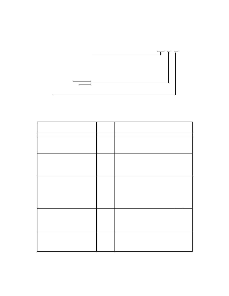
Table 2�1. Direct Register Map
RS2
RS1
RS0
REGISTER ADDRESSED BY MPU
R / W
DEFAULT (HEX)
0
0
0
Palette Address Register � Write Mode
R / W
XX
0
0
1
Color Palette Holding Register
R / W
XX
0
1
0
Pixel Read Mask
R / W
FF
0
1
1
Palette Address Register � Read Mode
R / W
XX
1
0
0
Reserved
XX
1
0
1
Reserved
XX
1
1
0
Index Register
R / W
XX
1
1
1
Data Register
R / W
XX
2�2
Table 2�2. Indirect Register Map (Extended Registers)
INDEX REGISTER
(HEX)
R / W
DEFAULT
(HEX)
REGISTER ADDRESSED
BY INDEX REGISTER
00
R / W
00
Cursor Position X LSB
01
R / W
00
Cursor Position X MSB
02
R / W
00
Cursor Position Y LSB
03
R / W
00
Cursor Position Y MSB
04
R / W
1F
Sprite Origin X
05
R / W
1F
Sprite Origin Y
06
R / W
00
Cursor Control Register
07
Reserved
08
W
XX
Cursor RAM Address LSB
09
W
XX
Cursor RAM Address MSB
0A
R / W
XX
Cursor RAM Data
0B
Reserved
0C � 0F
Reserved-Undefined
10
R / W
XX
Window Start X LSB
11
R / W
XX
Window Start X MSB
12
R / W
XX
Window Stop X LSB
13
R / W
XX
Window Stop X MSB
14
R / W
XX
Window Start Y LSB
15
R / W
XX
Window Start Y MSB
16
R / W
XX
Window Stop Y LSB
17
R / W
XX
Window Stop Y MSB
18
R / W
80
Multiplexer Control Register 1
19
R / W
98
Multiplexer Control Register 2
1A
R / W
00
Input-Clock Selection Register
1B
R / W
3E
Output-Clock Selection Register
1C
R / W
00
Palette Page Register
1D
R / W
20
General Control Register
1E
R / W
00
Configuration Register
1F
Reserved-Undefined
20
R / W
XX
Overscan Color Red
21
R / W
XX
Overscan Color Green
NOTE 1: Reserved registers should be avoided; otherwise, circuit behavior could deviate
from that specified. Reserved-undefined registers are nonexistent locations on
the register map.

2�3
Table 2�2. Indirect Register Map (Extended Registers) (Continued)
INDEX REGISTER
(HEX)
R / W
DEFAULT
(HEX)
REGISTER ADDRESSED
BY INDEX REGISTER
22
R / W
XX
Overscan Color Blue
23
R / W
XX
Cursor Color 0, Red
24
R / W
XX
Cursor Color 0, Green
25
R / W
XX
Cursor Color 0, Blue
26
R / W
XX
Cursor Color 1, Red
27
R / W
XX
Cursor Color 1, Green
28
R / W
XX
Cursor Color 1, Blue
29
R / W
09
Auxiliary-Control Register
2A
Reserved
2B
Reserved
2C
Reserved
2D
Reserved
2E
Reserved
2F
Reserved
30
R / W
XX
Color-Key OL/VGA Low
31
R / W
XX
Color-Key OL/VGA High
32
R / W
XX
Color-Key Red Low
33
R / W
XX
Color-Key Red High
34
R / W
XX
Color-Key Green Low
35
R / W
XX
Color-Key Green High
36
R / W
XX
Color-Key Blue Low
37
R / W
XX
Color-Key Blue High
38
R / W
10
Color-Key Control Register
39
Reserved-Undefined
3A
R / W
00
Sense-Test Register
3B
R
XX
Test-Data Register
3C
R
XX
CRC LSB
3D
R
XX
CRC MSB
3E
W
XX
CRC Control Register
3F
R
10
ID Register
FF
W
XX
Reset Register
NOTE 1: Reserved registers should be avoided; otherwise, circuit behavior could deviate
from that specified. Reserved-undefined registers are nonexistent locations on
the register map.

2�4
2.2
Color Palette
The color palette is addressed by an internal 8-bit address register for reading/writing data from/to the RAM.
This register is automatically incremented following a RAM transfer, allowing the entire palette to be
read/written with only one access of the address register. When the address register increments beyond
the last location in RAM, it is reset to the first location (address 0). All read and write accesses to the RAM
are asynchronous to SCLK, VCLK, and dot clock but performed within one dot clock. Therefore, they do not
cause any noticeable disturbance on the display.
The color RAM is 24 bits wide for each location and 8 bits wide for each color. Since the MPU access is
8 bits wide, the color data stored in the palette is 8 bits even when the 6-bit mode is chosen
(8/6 = 0). If the 6-bit mode is chosen, the 2 MSBs of color data in the palette have the values previously
written. However, if they are read back in the 6-bit mode, the 2 MSBs are 0s to be compatible with IMSG176
and Bt176. The output multiplexer shifts the six LSB to the six MSB positions and fills the 2 LSBs with 0s
after the color palette. The multiplexer then feeds the data to the DAC. The test register and the CRC
calculation both take data after the output multiplexer, enabling total system verification. The color-palette
access is described in the following two sections, and it is fully compatible with IMSG176/8 and Bt476/8.
2.2.1
Writing to Color-Palette RAM
To load the color palette, the MPU must first write to the address register (write mode) with the address where
the modification is to start. This is then followed by three successive writes to the palette-holding register
with 8 bits of red, green, and blue data. After the blue write cycle, the three bytes of color data are
concatenated into a 24-bit word that is then written to the RAM location specified by the address register.
The address register then increments to the next location, which the MPU may modify by simply writing
another sequence of red, green, and blue data. A block of color values in consecutive locations may be
written to by writing the start address and performing continuous red, green, and blue write cycles until the
entire block has been written.
2.2.2
Reading From Color-Palette RAM
Reading from the palette is performed by writing to the address register (read mode) with the location to be
read. This then initiates a transfer from the palette RAM into the holding register, followed by an increment
of the address register. Three successive MPU reads from the holding register produce red, green, and blue
color data (6 or 8 bits depending on the 8/6 mode) for the specified location. Following the blue read-cycle,
the contents of the color-palette RAM at the address specified by the address register are copied into the
holding register and the address register is again incremented. As with writing to the palette, a block of color
values in consecutive locations may be read by writing the start address and performing continuous red,
green, and blue read-cycles until the entire block has been read. Since the color-palette RAM is dual ported,
the RAM may be read during active display without disturbing the video.
2.2.3
Palette Page Register
The palette page register appears as an 8-bit register on the extended register map (see Section 2.1). Its
purpose is to provide high-speed color changing by removing the need for palette reloading. When using
1, 2, or 4 bit-planes, the additional planes are provided from the page register. When using four bit-planes,
the pixel inputs specify the lower 4 bits of the palette address with the upper 4 bits specified from the page
register. This gives the user the capability of selecting from 16 palette pages with only one-chip access, thus
allowing all the screen colors to be changed at the line frequency. A bit-to-bit correspondence is used;
therefore, in the above configuration, page-register bits 7 through 4 map onto palette-address bits 7 through
4, respectively. This is illustrated in Table 2�3.
2�5
NOTE:
The additional bits from the page register are inserted after the read mask.
The palette page register specifies the additional bit-planes for the overlay field in
direct-color modes with less than 8 bits per pixel overlay.
Table 2�3. Allocation of Palette Page Register Bits
NUMBER OF BIT PLANES
MSB
PALETTE-ADDRESS BITS
LSB
8
M
M
M
M
M
M
M
M
4
P7
P6
P5
P4
M
M
M
M
2
P7
P6
P5
P4
P3
P2
M
M
1
P7
P6
P5
P4
P3
P2
P1
M
M = bit from pixel port
Pn = n bit from page register
2.2.4
Read Masking
The read-mask register is an 8-bit register used to enable or disable a bit-plane from addressing the
color-palette RAM in the pseudo-color modes. Each palette address bit is logically ANDed with the
corresponding bit from the read mask register before going to the palette page register and addressing the
palette RAM.
In order to provide maximum flexibility to control palette data, the read mask operation is performed before
the addition of the page register bits. Therefore, care must be taken in those modes that have less than 8
bits per pixel of pseudo-color or overlay data. Be aware of the palette page register settings in these modes.
2.3
Clock Selection and Output-Clock (SCLK, RCLK, and VCLK) Generation
The TVP3010C and the TVP3010M VIP provide a maximum of five clock inputs. CLK0 is dedicated as a
TTL input. The other four clock inputs can be selected as either two differential ECL input or two extra TTL
inputs. The TTL inputs can be used for video rates up to 140 MHz. The dual-mode clock input (ECL / TTL)
is primarily an ECL input but can be used as TTL-compatible inputs if the input-clock selection register is
so programmed. The clock source used at power up is CLK0; an alternative source can be selected by
software during normal operation. This chosen clock input can be used unmodified as the dot clock
(representing pixel rate to the monitor). Alternatively, when the input-clock selection register is programmed
to use the internal frequency-doubler, the chosen clock source is used as a reference for multiplication. Each
device also allows for user programming of RCLK, SCLK and VCLK outputs (reference, shift and video
clocks) by using the output-clock selection register. The input-clock and output-clock selection registers are
located in the indirect register map (see Table 2�2).
The ECL inputs can be used as differential or single-ended inputs. When CLK1 or CLK3 is used as a
single-ended ECL input, CLK2 or CLK4 needs to be externally terminated to set the input common-mode
signal level. This can be done with a simple resistor divider, as is the case with fully differential ECL. Care
needs to be taken when choosing the resistor values to ensure that the dc level on CLK2 or CLK4 is in the
middle of the CLK1 or CLK3 ECL-input signal range.
2.3.1
RCLK, SCLK, VCLK
Both VIP devices provide a user-programmable reference clock (RCLK), a shift clock (SCLK), and video
(VCLK) clock outputs that can be set as divisions of the dot clock. RCLK is a continuously-running reference
clock and is not disabled during the Blank signal. RCLK can be selected as divisions of 1, 2, 4, 8, 16, 32 or
64 of the

2�6
dot clock (see Table 2�4). It is provided as a clock reference and is typically connected back to the LCLK
input to latch pixel-port data. Since pixel-port data is latched on the rising edge of LCLK, the RCLK frequency
must be set as a function of the desired multiplexing ratio (that depends on the pixel-bus width and number
of bit-planes, see Section 2.4).
Table 2�4. Output-Clock Selection Register Format
OUTPUT-CLOCK SELECTION-REGISTER BITS (see Note 2)
FUNCTION (see Notes 2 3 4 and 5)
6
5
4
3
2
1
0
FUNCTION (see Notes 2, 3, 4, and 5)
0
0
0
x
x
x
VCLK /1 output ratio
0
0
1
x
x
x
VCLK /2 output ratio
0
1
0
x
x
x
VCLK /4 output ration
0
1
1
x
x
x
VCLK /8 output ratio
1
0
0
x
x
x
VCLK /16 output ratio
1
0
1
x
x
x
VCLK /32 output ratio
1
1
0
x
x
x
VCLK /64 output ratio
1
1
1
x
x
x
VCLK output held at logic 1
x
x
x
0
0
0
RCLK /1 output ratio (see Notes 2 and 5)
x
x
x
0
0
1
RCLK /2 output ratio (see Notes 2 and 5)
x
x
x
0
1
0
RCLK /4 output ratio (see Notes 2 and 5)
x
x
x
0
1
1
RCLK /8 output ratio (see Notes 2 and 5)
x
x
x
1
0
0
RCLK /16 output ratio (see Notes 2 and 5)
x
x
x
1
0
1
RCLK /32 output ratio (see Notes 2 and 5)
x
x
x
1
1
0
RCLK /64 output ratio (see Notes 2 and 5)
0
x
x
x
1
1
0
RCLK /64, SCLK output held at logic 0
0
x
x
x
1
1
1
RCLK, SCLK outputs held at logic 0
x
1
1
1
1
1
1
Clock counter reset (6)
These lines indicate the reset conditions as required for VGA pass-through.
NOTES:
2. Register bit 6 enables (1) and disables (default = 0) the SCLK output buffer. Register bit 7 is a don't
care bit.
3. When the clocks are selected from one mode to the other, a minimum of 30 ns is needed before
the new clocks are stabilized and running.
4. When the output-clock-selection register is written with 3F (hex), the clock counter is reset,
RCLK = SCLK = 0, and VCLK = 1.
5. SCLK is the same as RCLK except that it is disabled during blank. When the RCLK divide ratio is
chosen, this sets the SCLK ratio as well.
SCLK is the same as RCLK but disabled during the Blank active period. SCLK is designed to be used as
the shift clock to interface directly with the VRAM. If SCLK is not used, the output can be switched off and
held low to protect against VRAM lockup due to invalid SCLK frequencies. The detailed SCLK control timing
is discussed in subsection 2.3.2.
VCLK is designed to be used as the timing reference by the graphics processor or other custom-designed
control logic to generate the graphics system control signals (SYSBL, HSYNC, and VSYNC). VCLK can be
selected as divisions of 1, 2, 4, 8, 16, 32, or 64 of the dot clock and can also be held at high (see Table 2�4).
The default setup is VCLK held at high since it is not used in VGA pass-through mode. Since these control
signals are sampled by VCLK, VCLK must be enabled for these to function properly.
Even though RCLK /SCLK and VCLK can be selected independently, there is still a relationship between
the two as discussed below. Many system considerations have been carefully covered in their design,
leaving maximum freedom to the user.

2�7
Internally, RCLK, SCLK, and VCLK are generated from a common clock counter that is counted at the rising
edge of the dot clock. Therefore, when VCLK is enabled, it is naturally in phase with RCLK and SCLK as
shown in Figure 2�1.
Normally, the video-control signal inputs HSYNC, VSYNC, and SYSBL are latched on the falling edge of
VCLK when in a non-VGA mode. When the configuration register is programmed for opposite VCLK polarity,
these video-control signals are latched on the rising edge of VCLK.
The internal clock counter is initialized any time the output-clock selection register is written with 3F (hex).
This provides a simple mechanism to synchronize multiple palettes or system devices by providing a known
phase relationship for the various system clocks. It is left up to the user to provide some means of disabling
the dot-clock input to the part while this reset is occurring if multiple parts are to be synchronized.
The reset default divide ratio for RCLK is 64:1 with SCLK held low and VCLK held at high. When choosing
certain video timing parameters, exercise caution if the selected RCLK frequency is less than the selected
VCLK frequency (see Appendix B for a more detailed discussion).
Dot Clock
VCLK
(dot clock/4 as an example)
RCLK = SCLK
(dot clock/2 as an example)
Figure 2�1. Dot Clock / VCLK / RCLK / SCLK Relationship
The input-clock-selection register selects the desired input-clock source. Table 2�5 details how to program
the various options.
Table 2�5. Input-Clock Selection Register
INPUT-CLOCK-SELECT REGISTER
(HEX) (see Note 6)
FUNCTION (see Note 7)
00
Select CLK0 as TTL-clock source
01
Select CLK1 as TTL-clock source
02
Select CLK2 as TTL-clock source
03
Select CLK3 as TTL-clock source
04
Select CLK4 as TTL-clock source
06
Select CLK3/CLK4 as ECL-clock source up to 140 MHz
07
Select CLK1/CLK2 as ECL-clock source up to device limit
10
Select CLK0 as doubled TTL-clock source
11
Select CLK1 as doubled TTL-clock source
12
Select CLK2 as doubled TTL-clock source
13
Select CLK3 as doubled TTL-clock source
14
Select CLK4 as doubled TTL-clock source
16
Select CLK3/CLK4 as doubled ECL-clock source
17
Select CLK1/CLK2 as doubled ECL-clock source
CLK0 is chosen at reset as required for VGA pass-through.
NOTES:
6. Register bits 3 and 7 are don't-care bits.
7. Register bits 5 and 6 are reserved.
8. When the clocks are selected from one input clock source to another, a minimum of 30 ns is needed before
the new clocks are stabilized and running.

2�8
The output-clock-selection register is used to program the desired divided-down frequencies for the
reference/shift and video clocks.
2.3.2
Frame-Buffer Clocking: Self-Clocked or Externally Clocked
The TVP3010C and the TVP3010M have two pixel-data latching modes, allowing for flexibility in the
frame-buffer interface timing. For the pixel port P(0 � 31), data is always latched on the rising edge of LCLK.
If auxiliary-control register (ACR) bit 3 is set to 1 (default), the internal circuitry is configured for self-clocked
mode. In this mode, the RCLK or SCLK output of the palette must be used as the timing reference to present
data to the pixel port P(0 � 31). In self-clocked mode, RCLK can be directly tied back to LCLK or LCLK can
be a delayed version of RCLK within the timing requirements of the VIP. The self-clocked mode of
frame-buffer latching is similar to the operation of the TLC3407X video-interface palette devices.
The VIP internal Blank signal is generated from either VGABL or SYSBL, depending on whether the VGA
port is enabled (multiplexer control register 2 (MCR2) bit 7 = 1) or disabled (MCR2 bit 7 = 0). The rising edge
of CLK0 latches VGABL when the VGA port is enabled. The falling edge of VCLK is used to sample and
latch the SYSBL input when the VGA port is disabled. When the internal Blank signal becomes active, SCLK
is disabled as soon as possible. For example, if SCLK is high when the sampled SYSBL goes low, SCLK
is allowed to complete the clock cycle and return to the low state. SCLK then is held low until the sampled
SYSBL signal goes back high. At this time, SCLK is enabled to clock the first pixel data valid from VRAM.
The VIP video-blanking circuitry is designed with sufficient pipeline delay to allow the internal sampled
SYSBL and VGABL signals to align with the pipelined RGB data to the video DACs. The logic described
previously works in situations where the SCLK period is shorter than, equal to, or longer than the VCLK
period.
When in the self-clocked mode, the SCLK control timing is designed to interface directly with the external
VRAM. The shift register in the system VRAM is supposed to be updated during the blank active period.
When the SYSBL input is sampled high by the falling edge of VCLK, the VRAM shift clock (SCLK) is restarted
to clock the VRAM and enable the first group of pixel data to appear on the pixel bus as well as at the
TVP3010 pixel input port. The second SCLK causes the VRAM shift register to shift out the second group
of data. At the same time, LCLK latches the first group of pixel data into the VIP (see Figure 2�2 for a detailed
timing-diagram).
VCLK
In Phase
SYSBL
at Input Terminal
LD
Internal Delayed
LCLK = RCLK
Blank
(internal signal
before dot-clock
pipeline delay)
Pixel Data
at Input Terminal
SCLK
Latch Last Group
of Pixel Data
Latch First Group of Pixel Data
Latch Last Group
of Pixel Data
Last Group of Pixel Data
1st
Group
2nd
Group
3rd
Group
4th
Group
5th
Group
6th
Group
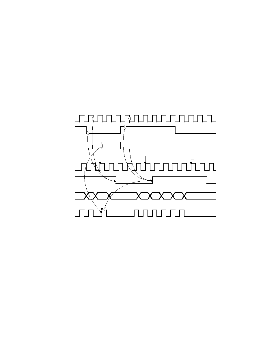
Figure 2�2. SCLK / VCLK Control Timing
(SSRT Disabled, RCLK / SCLK Frequency = VCLK Frequency)
The RCLK / SCLK phase relationship is designed so that timing specifications are satisfied for the case
where SCLK is driving a typical 2-MB VRAM load and RCLK is connected to LCLK. If an external buffer is
2�9
required on SCLK so that it can drive a larger load, a similar buffer can be placed on RCLK to match the
signal delay before connecting to LCLK. However, the delay from LCLK to RCLK cannot exceed one RCLK
period � 7 ns, (see the timing-parameter specifications for more details).
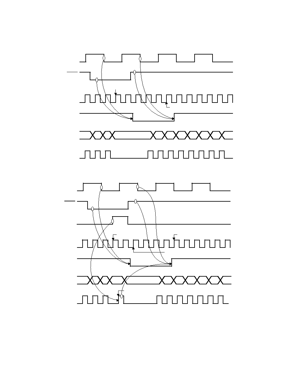
When the VRAM split shift register operation is performed (see Figure 2�3 and Figure 2�4), the SCLK timing
is adjusted to work with the SFLAG input. Basically, the split shift register operation inserts an SCLK during
the blank period. This causes the first group of pixel data to appear at the pixel port during blank and allows
the first group of data to be displayed as soon as the palette comes out of blank. Figures 2�3 and 2�5 show
the case when the SSRT (split shift register transfer) function is enabled. When a rising edge occurs on the
SFLAG input, one SCLK with a minimum 15-ns pulse duration is generated after the specified delay. Since
this is designed to meet VRAM timing requirements, the SSRT-generated SCLK replaces the first SCLK in
the regular shift register transfer case as described above (see Section 2.15 for a detailed explanation of
the SSRT function).
VCLK
In Phase
SYSBL
at Input Terminal
LD
Internal Delayed
LCLK = RCLK
Blank
(internal signal
before dot-clock
pipeline delay)
Pixel Data
at Input Terminal
SCLK
Latch Last Group
of Pixel Data
Latch First Group of Pixel Data
Latch Last Group
of Pixel Data
SFLAG Input
Last
Group
2nd
Group
3rd
Group
4th
Group
5th
Group
6th
Group
1st Group of
Pixel Data
SCLK Between Split Shift-Register and Regular Shift-Register Transfer
Figure 2�3. SCLK/VCLK Control Timing
(SSRT Enabled, RCLK/SCLK Frequency = VCLK Frequency)
2�10
VCLK
In Phase
SYSBL
at Input Terminal
LD
Internal Delayed
LCLK = RCLK
Blank
(internal signal
before dot-clock
pipeline delay)
Pixel Data
at Input Terminal
SCLK
Latch Last Group
of Pixel Data
Latch first Group of Pixel Data
1st
Group
2nd
Group
3rd
Group
4th
Group
5th
Group
6th
Group
Last Group of Pixel Data
7th
Group
Figure 2�4. SCLK/VCLK Control Timing
(SSRT Disabled, RCLK/SCLK Frequency = 4 x VCLK Frequency)
VCLK
In Phase
SYSBL
at Input Terminal
LD
Internal Delayed
LCLK = RCLK
Blank
(internal signal
before dot-clock
pipeline delay)
Pixel Data
at Input Terminal
SCLK
Latch Last Group
of Pixel Data
Latch First Group of Pixel Data
2nd
Group
3rd
Group
4th
Group
5th
Group
6th
Group
First Group of Pixel Data
7th
Group
Last
Group
Latch Second Group
of Pixel Data
SCLK Between Split Shift-Register Transfer and Regular Shift-Register Transfer
SFLAG Input
Figure 2�5. SCLK/VCLK Control Timing
(SSRT Enabled, RCLK/SCLK Frequency = 4 x VCLK Frequency)

2�11
Externally clocked timing can be chosen for the pixel bus P(10 � 31) by clearing auxiliary control register bit 3
to 0. In externally clocked mode, the RCLK or SCLK output of the palette is not used as the timing reference
to present data to the pixel bus. Instead, pixel data is presented to the palette with a synchronous clock and
all palette timing is referenced to this clock. In this mode, the external clock should be connected to LCLK
and the selected clock input. (When the VGA port is enabled, the CLK0 input is selected independent of the
input-clock selection register.)
The externally clocked frame-buffer interface mode is intended for applications where windowed or
pixel-by-pixel switching between the VGA port and the pixel port is desired in non-VRAM-based graphics
systems. In such applications, the VGA port is enabled (multiplexer control register bit 7 set to 1) and the
appropriate direct-color mode is set in the multiplexer control register. The auxiliary-window, port-select,
and/or color-key switching functions are then configured and enabled to perform the desired switching. By
setting the frame-buffer interface to the externally clocked mode, the pixel port and VGA port timing and
pipeline delay are made the same. Also, since the VGA port is enabled, all video-control signal timing is
referenced to CLK0, utilizing the VGABL, HSYNC, and VSYNC inputs.
The externally clocked frame-buffer interface timing can also be used in non-VGA switching applications,
utilizing only the pixel port or only the VGA port. In either case, it is recommended that VGA video-control
signals be used (i.e., VGABL, HSYNC, VSYNC). In this way, all pixel data and video-control signals are
referenced to CLK0 and video blank and sync are aligned with pixel data.
NOTE:
When the pixel port is used in externally clocked mode (ACR3 = 0), RCLK must be
set to VCLK/1 (DOT/1) in the output-clock selection register and a 1:1 multiplexing
mode must be selected in the multiplexer control registers (see Table 2�6). The
external clock should be connected to the LCLK input as well as the selected clock
input. When the VGA port is also enabled (MCRB7 = 1), CLK0 is selected as the
input clock independent of the input-clock selection-register setting.
VGA switching can only be performed using a 1:1 multiplexing mode.
Overlay switching can only be performed using a 1:1 multiplexing mode when the
pixel port is set for externally clocked mode. When the pixel port is self-clocked, any
of the multiplex ratios may be used (see subsection 2.4.6).
When VGA switching is to be performed using externally clocked mode
(ACR3 = 0), the full VGA port frequency of 85 MHz may be utilized provided that
the VGA port and the pixel port are both synchronized to the CLK0 input clock.
If VGA switching is to be performed using self-clocked mode (ACR3 = 1), the
maximum pixel rate cannot exceed 50 MHz. This is because of internal delay from
the CLK0 input to the RCLK output. For external clocked timing, the LCLK input
needs to be enabled on terminal 73 (TVP3010C) or terminal L3 (TVP3010M) by
programming the configuration register bit 5 to 1.
VGA-data pipeline delay is adjusted within each VIP depending on whether self-
or externally clocked frame-buffer interface timing is used (see subsection 2.3.2 ).
If the VIP is programmed for self-clocked timing, three additional dot-clock pipeline
delays are inserted into the internal VGA-data path and into the internal blanking
signal. The additional pipeline delay accounts for the difference between VGABL
or SYSBL and the pixel-data inputs P(0 � 31) when used in the self- and externally
clocked modes. This is so the VGA and pixel-port data remain synchronous in time
when doing auxiliary window, port select, or color-keyed switching (see Section
2.6). When externally clocked timing is used, the VGA port and the pixel port are
already synchronous since both data and blanking are presented to the palette
during the same CLK0 clock cycle.

2�12
2.4
Multiplexing Scheme
Both the TVP3010C and TVP3010M palettes offer a highly versatile multiplexing scheme as illustrated in
Tables 2�6 through 2�11. The multiplexing scheme allows the pixel bus to be programmed to 1, 2, 4, 8, 12,
16, 24, or 32 bits/pixel with pixel-bus widths ranging from 1 bit to 32 bits. The use of on-chip multiplexing
allows graphics systems to be designed that can support multiple-pixel depths and resolutions with no
hardware modification. It also allows the system to be configured to the amount of RAM available. For
example, when only 256K bytes of memory are available, an 800
�
600 mode with four bit-planes (4 bits
per pixel) could be implemented using an 8-bit-wide pixel bus. If at a later date another 256K bytes are added
to another 8 bits of the pixel bus, the user has the option of using eight bit-planes at the same resolution or
four bit-planes at a 1024
�
768 resolution. When a further 512K bytes are added to the remaining 16 bits
of the pixel bus, the user has the option of eight bit-planes at 1024
�
768 or four bit-planes at 1280
�
1024.
Each VIP can also be configured for direct-color or true-color operation. All of the above can be achieved
without any board-level hardware modification and without any increase in the speed of the pixel bus.
Multiplexing of the pixel bus is controlled by and programmed through multiplexer control registers 1 and
2. For details of the multiplexer control register settings for each mode of operation, (see subsections 2.4.2
through 2.4.6).
2.4.1
Little-Endian and Big-Endian Data Format
The pixel bus on both the TVP3010C and TVP3010M supports both little-endian and big-endian data
formats for all pseudo-color, direct-color, and true-color modes of operation. The data-format select is
controlled by general control register-bit 3 (see subsection 2.16.2). When general control register (GCR)
bit 3 is cleared to 0 (default), then the format is set to little endian. When GCR bit 3 is set to 1, then the format
is set to big endian.
In a big-endian design, the external VRAM data-bus bits must be connected in reverse order to the VIP pixel
bus; i.e., D31 connected to P0, D0 connected to P31, etc. This ensures that the least-significant channel
always provides the first pixel to be displayed in the pseudo-color or true-color multiplexing modes. The
difference between little- and big-endian data formats and how they affect the pixel-bus operation is
discussed in detail in Appendix C.
2.4.2
VGA Pass-Through Mode
The TVP3010C and TVP3010M feature VGA pass-through mode.The VGA pass-through mode is used to
emulate the VGA modes of most personal computers. The advantage of this mode is that it can take data
presented on the feature connector of most VGA-compatible PC systems into the device on a separate bus,
thus requiring no external multiplexing. This feature is particularly useful in systems where the existing
graphics circuitry is on the motherboard. In this instance, it enables a drop-in graphics card to be
implemented that maintains compatibility with all existing software. This is accomplished by using the
on-board VGA circuitry but routing the emerging bit-plane data through the VIP. VGA pass-through is the
default mode at power up or reset.
Since this mode is designed with the feature connector philosophy, all data latching and control timing is
referenced to CLK0. When the VGA port is enabled (MCR2 bit 7 = 1), CLK0 is selected as the input clock
source independent of the input-clock-selection register. The VGA port always operates as in the externally
clocked mode of the pixel port P(0 � 31); it receives the VGA data [VGA(0 � 7)] and the VGA blank (VGABL),
both of which are referenced to an external clock (CLK0). CLK0 also latches the VGABL, HSYNC, and
VSYNC video-control signals when in the VGA pass-through mode. External signals on LCLK have no effect
on the VGA port since LCLK only latches data on the pixel port P(0 � 31).
VGA data pipeline delay is adjusted within the VIP depending on whether self- or externally clocked
frame-buffer interface timing is used (see subsection 2.3.2). When either device is programmed for
self-clocked timing, additional dot-clock pipeline delay is inserted into the internal VGA data path; this
permits the VGA and pixel-port data to remain synchronous when doing auxiliary window, port select, or
color-keyed switching (see Section 2.6). The additional VGA-pipeline delay accounts for the dot-
clock-to-RCLK pipeline delay within the palette.

2�13
2.4.3
Pseudo-Color Mode
In pseudo-color mode (sometimes called color indexing), the TVP3010C and TVP3010M pixel-bus inputs
are used to address the palette-RAM LUT (color-lookup table). The data in each RAM location is comprised
of 24 bits (8 bits for each of the red, green, and blue color DACs). The pseudo-color mode is further grouped
into 4 submodes, depending on the data bits per pixel. In each submode, a pixel bus width of 4, 8, 16, or
32 bits may be used. Data should always be presented on the least significant bits of the pixel bus; i.e., when
16 bits are used, the pixel data must be presented on P(15 � 0), 8 bits on P(7 � 0), and 4 bits on P(3 � 0) (see
subsection 2.4.6 for more details).
Submode 1 uses a single bit-plane to address the color palette. The pixel port bit is fed into bit 0 of the palette
address, with the 7 high-order address bits defined by the palette page register (see subsection 2.2.3). This
mode has uses in high-resolution monochrome applications such as desktop publishing. This mode allows
the maximum amount of multiplexing with 32:1 ratio, thus giving a pixel bus rate of only 4 MHz at a screen
resolution of 1280
�
1024. Although only a single bit is used, alteration of the palette page register at the
line frequency allows 256 different colors to be displayed on each screen with two colors for each line.
Submode 2 uses two bit-planes to address the color palette. The 2 bits are fed into the low-order address
bits of the palette with the six high-order address bits being defined by the palette page register (see
subsection 2.2.3). This mode allows a maximum multiplex ratio of 16:1 on the pixel bus and is essentially
a four-color alternative to submode 1.
Submode 3 uses four bit-planes to address the color palette. The 4 bits are fed into the low-order address
bits of the palette with the four high-order address bits being defined by the palette page register (see
subsection 2.2.3). This mode provides 16 pages of 16 colors and can be used at multiplex ratios of /1 to /8.
Submode 4 uses 8 bit-planes to address the color palette. Since all 8 bits of palette address are specified
from the pixel port, the page register is not used. This mode allows dot clock-to-LCLK ratios of 1:1 (8-bit bus),
2:1 (16-bit bus), or 4:1 (32-bit bus). Therefore, in a 32-bit configuration, a 1024
�
768 pixel screen can be
implemented with an external data rate of only 16 MHz.
NOTE:
When externally clocked frame-buffer timing is used (ACR3 = 0, see subsection
2.3.2), only multiplex ratios of 1:1 can be used (see subsection 2.4.6).
The auxiliary-window, port-select, and color-key switching functions must be
disabled and set for palette graphics when in the pseudo-color mode. This is the
default condition at reset (see Section 2.6)
.
2.4.4
Direct-Color Mode
When either VIP is operated in direct-color mode, 24, 16, 15, or 12 bits of data can be transferred directly
to the RGB DACs but with the same amount of pipeline delay as the overlay data and the control signals
(Blank and Syncs). Depending on which direct-color mode is selected, overlay is provided by utilizing the
remaining bits of the pixel bus to address the palette RAM. This results in a 24-bit RAM output that is then
used as overlay information to the DACs. The overlay capability is designed to work with the
auxiliary-window, port-select, and color-key switching functions to provide overlay in specific windows or
on a pixel-by-pixel basis on the direct-color display as discussed in Section 2.6 (see subsection 2.4.6 for
more details on selecting the direct-color modes).
The default condition after reset is for the auxiliary-window and port-select functions to be disabled
(ACR1 = ACR2 = 0). The color-key comparisons, which are controlled by the color-key control (CKC)
register bits 0 � 3, are also disabled (CKC0 = CKC1 = CKC2 = CKC3 = 0). Also, since multiplexer control
register 2 bit 7 = 1 and ACR0 = CKC4 = 1 at reset, the default is for VGA pass-through. This is because
multiplexer control register 2 bit 7 enables the VGA port and the switching functions (switch = color key =
1, see Section 2.6) are disabled and set for palette graphics as opposed to direct-color palette bypass.
Submode 1 is the 24-bit direct-color mode that uses 8 bits to represent each color and 8 bits for overlay. In
this mode, there are basically two different configurations: the 32-bit data is grouped either as overlay, red,
green, blue, or blue, green, red, overlay.

2�14
Submode 2 is the XGA-compatible (5 � 6 � 5) 16-bit color mode supporting 5 bits of red, 6 bits of green, and
5 bits of blue data. Both VIPs support multiplex ratios for this mode of 1:1 and 2:1. With 2:1 multiplexing,
the TVP3010 can display 1024 x 768 direct color using 45-MHz VRAM without any glue logic. Overlay is not
available in this mode.
Submode 3 is the TARGA-compatible (5 � 5 � 5) mode that uses 15 bits for color and 1 bit for overlay. It allows
5 bits for each of red, green, and blue data. The TVP3010C and the TVP3010M support 1:1 and 2:1
multiplexing ratios in this mode.
Submode 4 is (6 � 6 � 4) configuration. It provides 6 bits of red, 6 bits of green, and 4 bits of blue. Both VIPs
also support 1:1 and 2:1 multiplexing in this mode. Overlay is not available in this mode.
Submode 5 is (4 � 4 � 4 � 4) configuration. It provides 12 bits of direct color and 4 bits of overlay. It allows 4
bits for each of red, green, and blue data. The TVP3010C and the TVP3010M support 1:1 and 2:1
multiplexing ratios in this mode (see NOTE in subsection 2.4.5).
2.4.5
True-Color Mode
In true-color mode, the palette RAM is partitioned into three independent 256-word
�
8-bit memory blocks
that can be individually addressed by each color field of the true-color data. The independent memory blocks
provide data for a single DAC output. With this architecture, gamma correction for each color is possible.
Since the palette is used in true-color mode, there is no memory space to be used for the overlay function.
All of the true-color submodes are the same as direct color except that overlay is not available. (see
Tables 2�6 through 2�11 for more details on mode selection and see NOTE below).
NOTE:
Since less than 8 bits are defined for each color in the various 12- or 16-bit direct-
or true-color modes, the data bits for the individual colors are internally shifted to
the MSB locations and the remaining LSB locations for each color are set 0 before
8-bit data is sent to the DACs.
Since the overlay information goes through the pseudo-color data path, it is subject
to read masking and the palette page register. This is especially important for those
direct-color modes that have less than eight bits of overlay information. The overlay
information in these modes justifies to the LSB bit positions, and the remaining
MSB positions are filled with the corresponding palette page data before
addressing the palette RAM.
In order to display true color (gamma corrected through the palette), either the
auxiliary windowing or the color-key switching function must be set for palette
graphics. For direct color, both functions must be set for direct color.
In order to use the overlay capability of the direct-color modes, the color-key
switching or port-select function must be configured and enabled. Overlay port data
in a window is also available by enabling the auxiliary window function. If either the
auxiliary windowing or the color-key switching functions point to palette graphics,
palette graphics are always displayed (not direct color).
When in the 24-bit direct-color or true-color modes, the data input works only in the
8-bit mode. In other words, when only 6 bits are used, the two LSB inputs for each
color need to be tied to GND. However, the palette, which is used by the overlay
input, is still governed by 8/6, and the output multiplexer selects 8 bits or 6 bits of
data accordingly. The 8/6 is also valid in the other 16-bit modes.
The definitions of direct color (palette bypass) and true color are consistent with the
IBM XGA terminology.
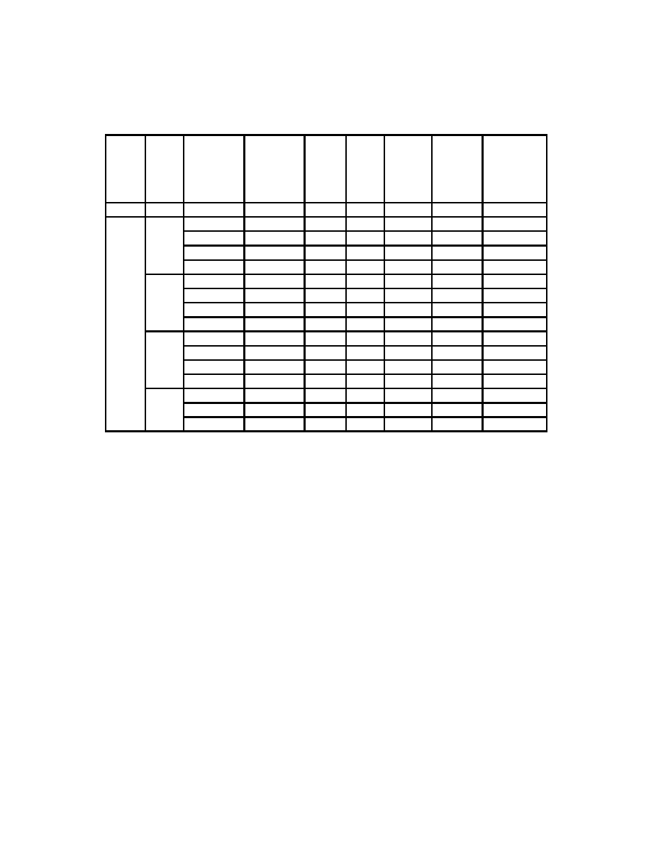
2�15
Table 2�6. Multiplex Mode and Bus-Width Selection
MODE
SUB-
MODE
MULTIPLEX-
CONTROL
REGISTER 1
(HEX)
MULTIPLEX-
CONTROL
REGISTER 2
(HEX)
DATA
BITS
PER
PIXEL
(see
Note 9)
PIXEL-
BUS
WIDTH
MULTI-
PLEX
RATIO
(see
Note 10)
OVERLAY
BITS
PER
PIXEL
TABLE
REFERENCE
(see
Note 11)
VGA
80
98
8
8
1
NA
v1
80
00
1
4
4
NA
s1
1
80
01
1
8
8
NA
s2
1
80
02
1
16
16
NA
s3
80
03
1
32
32
NA
s4
80
08
2
4
2
NA
s6
2
80
09
2
8
4
NA
s7
P
d
2
80
0A
2
16
8
NA
s8
Pseudo
Color
80
0B
2
32
16
NA
s9
Color
80
10
4
4
1
NA
s11
3
80
11
4
8
2
NA
s12
3
80
12
4
16
4
NA
s13
80
13
4
32
8
NA
s14
80
19
8
8
1
NA
s16
4
80
1A
8
16
2
NA
s17
80
1B
8
32
4
NA
s18
NOTES:
9. Data bits per pixel is the number of bits of pixel-port information used as color data for each displayed pixel,
often referred to as the number of bit-planes.
10. Multiplex ratio indicates the number of pixels per bus load or the number of pixels associated with each
LCLK (load clock) pulse. For example, with a 32-bit pixel-bus width and eight bit-planes, each bus load
consists of four pixels. In a typical implementation, the LCLK signal is either connected to or derived from
RCLK. Therefore, the RCLK divide ratio must be chosen as a function of the multiplex mode selected. The
RCLK divide ratio is not automatically set by mode selection but must be programmed in the output-clock
selection register by the user.
11. This column is a reference to Tables 2�7 through 2�11, where the actual manipulation of pixel information
and pixel latching sequences are illustrated for each of the multiplexing modes.
12. It is recommended that all unused input terminals be connected to ground to conserve power.
13. Multiplexer control register 2 bit 7 enables (1) and disables (0) the VGA port. When auxiliary-window or
port-select switching is to be done involving the VGA port, this bit needs to be set to 1 as well as
programming for the correct direct-color mode. For example, when auxiliary windowing is to be done with
direct-color submode 1 (32-bit pixel bus) and VGA, instead of programming 1B (hex), multiplexer control
register 2 should be programmed to 9B (hex). When only VGA pass-through is desired, the values should
be programmed for VGA mode as indicated in Table 2�6. When only VGA pass-through is desired, the
values should be programmed as indicated in Table 2�6 for VGA mode.
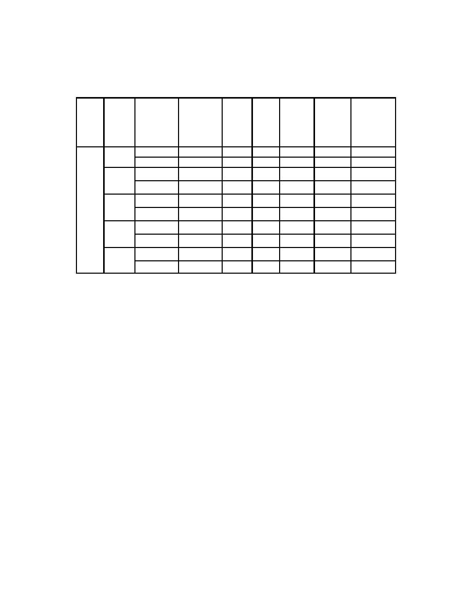
2�16
Table 2�6. Multiplex Mode and Bus-Width Selection (Continued)
MODE
SUB-
MODE
MULTIPLEX-
CONTROL
REGISTER 1
(HEX)
MULTIPLEX-
CONTROL
REGISTER 2
(HEX)
DATA
BITS
PER
PIXEL
(see
Note 9)
PIXEL-
BUS
WIDTH
MULTI-
PLEX
RATIO
(see
Note 10)
OVERLAY
BITS
PER
PIXEL
TABLE
REFERENCE
(see
Note 11)
1
06
1B
24
32
1
8
d1
24-bit
07
1B
24
32
1
8
d3
2
(5 6 5)
05
02
16
16
1
NA
d5
(5 � 6 � 5)
XGA
05
03
16
32
2
NA
d6
3
(5 5 5)
04
02
15
16
1
1
d8
Direct
(5 � 5 � 5)
TARGA
04
03
15
32
2
1
d9
4
16 bit
03
02
16
16
1
NA
d11
16-bit
(6 � 6 � 4)
03
03
16
32
2
NA
d12
5
12 bit
01
12
12
16
1
4
d14
12-bit
(4 � 4 � 4)
01
13
12
32
2
4
d15
NOTES:
9. Data bits per pixel is the number of bits of pixel-port information used as color data for each displayed pixel,
often referred to as the number of bit-planes.
10. Multiplex ratio indicates the number of pixels per bus load or the number of pixels associated with each
LCLK (load clock) pulse. For example, with a 32-bit pixel-bus width and eight bit-planes, each bus load
consists of four pixels. In a typical implementation, the LCLK signal is either connected to or derived from
RCLK. Therefore, the RCLK divide ratio must be chosen as a function of the multiplex mode selected. The
RCLK divide ratio is not automatically set by mode selection but must be programmed in the output-clock
selection register by the user.
11. This column is a reference to Tables 2�8 through 2�11, where the actual manipulation of pixel information
and pixel latching sequences are illustrated for each of the multiplexing modes.
12. It is recommended that all unused input terminals be connected to ground to conserve power.
13. Multiplexer control register 2 bit 7 enables (1) and disables (0) the VGA port. When auxiliary-window or
port-select switching is to be done involving the VGA port, this bit needs to be set to 1 as well as
programming for the correct direct-color mode. For example, when auxiliary windowing is to be done with
direct-color submode 1 (32-bit pixel bus) and VGA, instead of programming 1B (hex), multiplexer control
register 2 should be programmed to 9B (hex). When only VGA pass-through is desired, the values should
be programmed for VGA mode as indicated in Table 2�6. When only VGA pass-through is desired, the
values should be programmed as indicated in Table 2�6 for VGA mode.

2�17
Table 2�6. Multiplex Mode and Bus-Width Selection (Continued)
MODE
SUB-
MODE
MULTIPLEX-
CONTROL
REGISTER 1
(HEX)
MULTIPLEX-
CONTROL
REGISTER 2
(HEX)
DATA
BITS
PER
PIXEL
(see
Note 9)
PIXEL-
BUS
WIDTH
MULTI-
PLEX
RATIO
(see
Note 10)
OVERLAY
BITS
PER
PIXEL
TABLE
REFERENCE
(see
Note 11)
1
46
03
24
32
1
NA
t1
24-bit
47
03
24
32
1
NA
t3
2
(5 6 5)
45
02
16
16
1
NA
t5
(5 � 6 � 5)
XGA
45
03
16
32
2
NA
t6
True
3
(5 5 5)
44
02
15
16
1
NA
t8
True
Color
(5 � 5 � 5)
TARGA
44
03
15
32
2
NA
t9
4
16 bit
43
02
16
16
1
NA
t11
16-bit
(6 � 6 � 4)
43
03
16
32
2
NA
t12
5
12 bit
41
02
12
16
1
NA
t14
12-bit
(4 � 4 � 4)
41
03
12
32
2
NA
t15
NOTES:
9. Data bits per pixel is the number of bits of pixel-port information used as color data for each displayed pixel,
often referred to as the number of bit-planes.
10. Multiplex ratio indicates the number of pixels per bus load or the number of pixels associated with each
LCLK (load clock) pulse. For example, with a 32-bit pixel-bus width and eight bit-planes, each bus load
consists of four pixels. In a typical implementation, the LCLK signal is either connected to or derived from
RCLK. Therefore, the RCLK divide ratio must be chosen as a function of the multiplex mode selected. The
RCLK divide ratio is not automatically set by mode selection but must be programmed in the output-clock
selection register by the user.
11. This column is a reference to Tables 2�8 through 2�11, where the actual manipulation of pixel information
and pixel latching sequences are illustrated for each of the multiplexing modes.
12. It is recommended that all unused input terminals be connected to ground to conserve power.
13. Multiplexer control register 2 bit 7 enables (1) and disables (0) the VGA port. When auxiliary-window or
port-select switching is to be done involving the VGA port, this bit needs to be set to 1 as well as
programming for the correct direct-color mode. For example, when auxiliary windowing is to be done with
direct-color submode 1 (32-bit pixel bus) and VGA, instead of programming 1B (hex), multiplexer control
register 2 should be programmed to 9B (hex). When only VGA pass-through is desired, the values should
be programmed for VGA mode as indicated in Table 2�6. When only VGA pass-through is desired, the
values should be programmed as indicated in Table 2�6 for VGA mode.
2�18
Table 2�7. Pseudo-Color Mode Pixel-Latching Sequence (see Notes 14 and 16)
v1
s1
s2
s3
s4
s6
s7
s8
VGA7�VGA0
P0
P0
P0
P0
P1, P0
P1 � P0
P1 � P0
P1
P1
P1
P1
P3, P2
P3 � P2
P3 � P2
P2
P2
P2
P2
P5 � P4
P5 � P4
P3
�
�
�
P7 � P6
�
�
�
�
�
P7
P15
P31
P15 � P14
s9
s11
s12
s13
s14
s16
s17
s18
P1 � P0
P3 � P0
P3 � P0
P3 � P0
P3 � P0
P7 � P0
P7 � P0
P7 � P0
P3 � P2
P7 � P4
P7 � P4
P7 � P4
P15 � P8
P15 � P8
P5 � P4
P11 � P8
P11 � P8
P23 � P16
�
P15 � P12
�
P31 � P24
�
�
P31 � P30
P31 � P28
NOTES: 14. The latching sequence is initiated by a rising edge on LCLK. For modes in which multiple groups of data
are latched, the LCLK rising edge latches all the groups and the pixel clock shifts them out starting with the
low-numbered group. For example, in pseudo-color submode 3 with a 16-bit pixel-bus width, the rising edge
of LCLK latches all the data groups shown above (s13) and the pixel clock shifts them out in the order
P(3 � 0), P(7 � 4), P(11 � 8), and P(15 � 12). Note that each line in each subtable above represents one pixel.
15. When in the big-endian format (GCR3 =1), the pixel bus is externally swapped by the user (i.e., D31
connected to P0, D0 connected to P31). Since data is always shifted out from low-numbered groups to
high-numbered groups, the external swapping of the pixel bus causes the groups to be shifted out in the
correct order. However, for modes with more than 1 bit per pixel, the bits in each data group are reversed
(LSB to MSB). This is internally corrected by the VIP input multiplexer. The differences between big- and
little-endian data formats and how they affect the pixel bus operation is discussed in more detail in
Appendix C.
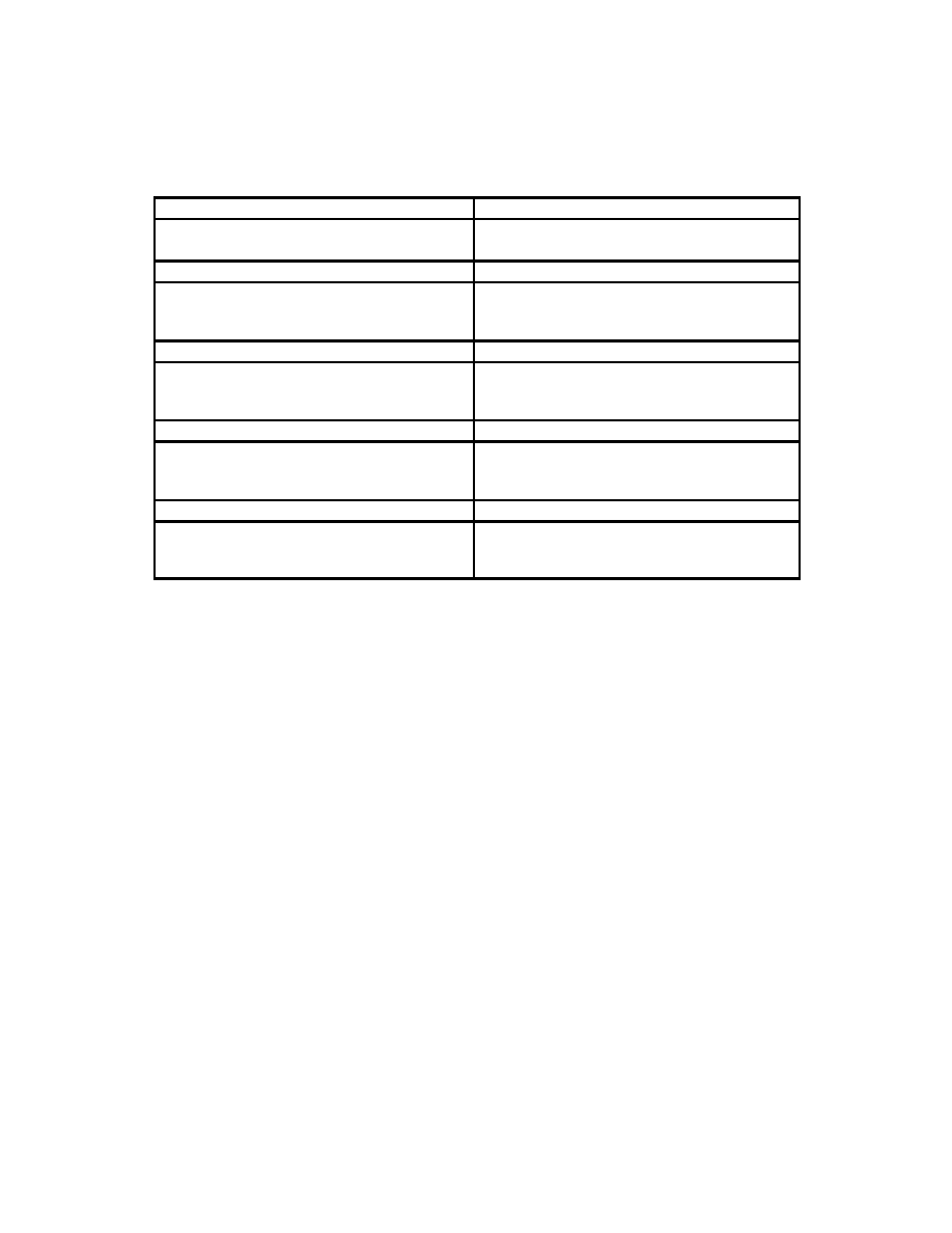
2�19
Table 2�8. Direct-Color Mode Pixel-Latching Sequence (Little Endian) (see Note 16)
d1
d3
P31 � P24(O), P23 � P16(R), P15 � P8(G), P7 � P0(B)
P31 � P24(B), P23 � P16(G), P15 � P8(R), P7 � P0(O)
MSB
LSB
MSB
LSB
d5
d6
P15 � P11(R), P10 � P5(G), P4 � P0(B)
P15 � P11(R), P10 � P5(G), P4 � P0(B)
P31 � P27(R), P26 � P21(G), P20 � P16(B)
MSB
LSB
MSB
LSB
d8
d9
P15(O), P14 � P10(R), P9 � P5(G), P4 � P0(B)
P15(O), P14 � P10(R), P9 � P5(G), P4 � P0(B)
P31(O), P30 � P26(R), P25 � P21(G), P20 � P16(B)
MSB
LSB
MSB
LSB
d11
d12
P15 � P10(R), P9 � P4(G), P3 � P0(B)
P15 � P10(R), P9 � P4(G), P3 � P0(B)
P31 � P26(R), P25 � P20(G), P19 � P16(B)
MSB
LSB
MSB
LSB
d14
d15
P15 � P12(R), P11 � P8(G), P7 � P4(B), P3 � P0(O)
P15 � P12(R), P11 � P8(G), P7 � P4(B), P3 � P0(O)
P31 � P28(R), P27 � P24(G), P23 � P20(B), P19 � P16(O)
MSB
LSB
MSB
LSB
NOTE 16: The latching sequence is initiated by a rising edge on LCLK. For modes in which multiple pixel-data groups
are latched on one LCLK rising edge, the pixel clock shifts them out starting with the low-numbered pixel data
group. Note that each line of each subtable above represents one pixel.

2�20
Table 2�9. Direct-Color Mode Pixel-Latching Sequence (Big Endian) (see Notes 17 and 18)
d1
d3
P31 � P24(B), P23 � P16(G), P15 � P8(R), P7 � P0(O)
P31 � P24(O), P23 � P16(R), P15 � P8(G), P7 � P0(B)
MSB
LSB
MSB
LSB
d5
d6
P15 � P11(B), P10 � P5(G), P4 � P0(R)
P15 � P11(B), P10 � P5(G), P4 � P0(R)
P31 � P27(B), P26 � P21(G), P20 � P16(R)
MSB
LSB
MSB
LSB
d8
d9
P15 � P11(B),P10 � P6(G),P5 � P1(R),P0(O)
P15 � P11(B), P10 � P6(G), P5 � P1(R), P0(O)
P31 � P27(B), P26 � P22(G), P21 � P17(R), P16(O)
MSB
LSB
MSB
LSB
d11
d12
P15 � P12(B), P11 � P6(G), P5 � P0(R)
P15 � P12(B), P11 � P6(G), P5 � P0(R)
P31 � P28(B), P27 � P22(G), P21 � P16(R)
MSB
LSB
MSB
LSB
d14
d15
P15 � P12(O), P11 � P8(B), P7 � P4(G), P3 � P0(R)
P15 � P12(O), P11 � P8(B), P7 � P4(G), P3 � P0(R)
P31 � P28(O), P27 � P24(B), P23 � P20(G),
P19 � P16(R)
MSB
LSB
MSB
LSB
NOTES: 17. The latching sequence is the same as in the little-endian example. Each line represents one pixel.
18. These subtables assume that the pixel bus is externally reverse-wired for big-endian mode operation (i.e.,
D31 connected to P0, D0 connected to P31) and that big-endian mode has been selected in the general-
control register (GCR3=1). The VIP internally corrects the bit ordering (LSB to MSB) for each pixel.
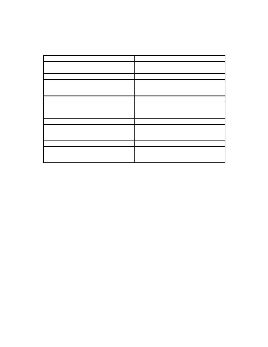
2�21
Table 2�10. True-Color Mode Pixel-Latching Sequence (Little Endian) (see Note 16)
t1
t3
P23 � P16(R), P15 � P8(G), P7 � P0(B)
P31 � P24(B), P23 � P16(G), P15 � P8(R)
MSB
LSB
MSB
LSB
t5
t6
P15 � P11(R), P10 � P5(G), P4 � P0(B)
P15 � P11(R), P10 � P5(G), P4 � P0(B)
P31 � P27(R), P26 � P21(G), P20 � P16(B)
MSB
LSB
MSB
LSB
t8
t9
P14 � P10(R),P9 � P5(G),P4 � P0(B)
P14 � P10(R), P9 � P5(G), P4 � P0(B)
P30 � P26(R), P25 � P21(G), P20 � P16(B)
MSB
LSB
MSB
LSB
t11
t12
P15 � P10(R), P9 � P4(G), P3 � P0(B)
P15 � P10(R), P9 � P4(G), P3 � P0(B)
P31 � P26(R), P25 � P20(G), P19 � P16(B)
MSB
LSB
MSB
LSB
t14
t15
P15 � P12(R), P11 � P8(G), P7 � P4(B)
P15 � P12(R), P11 � P8(G), P7 � P4(B)
P31 � P28(R), P27 � P24(G), P23 � P20(B)
MSB
LSB
MSB
LSB
NOTE 16: The latching sequence is initiated by a rising edge on LCLK. For modes in which multiple pixel data groups
are latched on one LCLK rising edge, the pixel clock shifts them out starting with the low-numbered pixel data
group. Note that each line in each subtable above represents one pixel.
2�22
Table 2�11. True-Color Mode Pixel-Latching Sequence (Big Endian) (see Notes 17 and 18)
t1
t3
P31 � P24(B), P23 � P16(G), P15 � P8(R)
P23 � P16(R), P15 � P8(G), P7 � P0(B)
MSB
LSB
MSB
LSB
t5
t6
P15 � P11(B), P10 � P5(G), P4 � P0(R)
P15 � P11(B), P10 � P5(G), P4 � P0(R)
P31 � P27(B), P26 � P21(G), P20 � P16(R)
MSB
LSB
MSB
LSB
t8
t9
P15 � P11(B),P10 � P6(G),P5 � P1(R)
P15 � P11(B), P10 � P6(G), P5 � P1(R)
P31 � P27(B), P26 � P22(G), P21 � P17(R)
MSB
LSB
MSB
LSB
t11
t12
P15 � P12(B), P11 � P6(G), P5 � P0(R)
P15 � P12(B), P11 � P6(G), P5 � P0(R)
P31 � P28(B), P27 � P22(G), P21 � P16(R)
MSB
LSB
MSB
LSB
t14
t14
P11 � P8(B), P7 � P4(G), P3 � P0(R)
P11 � P8(B), P7 � P4(G), P3 � P0(R)
P27 � P24(B), P23 � P20(G), P19 � P16(R)
MSB
LSB
MSB
LSB
NOTES: 17. The latching sequence is the same as in the little-endian example. Each line represents one pixel.
18. These subtables assume that the pixel bus is externally reverse wired for big-endian mode operation (i.e.,
D31 connected to P0, D0 connected to P31) and that big-endian mode has been selected in the general-
control register (GCR3 = 1). The VIP internally corrects the bit ordering (LSB to MSB) for each pixel.
2.4.6
Multiplexer Control Registers
The pixel-port multiplexer is controlled by two 8-bit registers in the indirect register-map (see Section 2.1).
The various multiplexing modes can be selected according to Table 2�6.

2�23
2.5
On-Chip Cursor
The TVP3010C and TVP3010M palettes have an on-chip two-color 64 x 64 pixel user-definable cursor. The
cursor operation defaults to the XGA standard, but X-Windows compatibility is also available (see
subsection 2.5.2). In addition to the 64
�
64 sprite cursor, both devices also support a two-color crosshair
cursor. The cursors only operate in noninterlaced applications.
The pattern for the 64
�
64 cursor is provided by the cursor RAM, which may be accessed by the MPU at
any time. Cursor positioning is performed using the cursor-position (X and Y) registers and the sprite origin
(X and Y) registers (see register-bit definitions in subsections 2.16.4 and 2.16.5). Positions X and Y are
defined in the palette increasing from left to right and from top to bottom, respectively, as seen on the display
screen. The cursor position (X and Y) is relative to the first pixel displayed. In other words, the very first pixel
displayed is located at position (0,0), and the last pixel displayed for a 1024
�
768 system is located at
position (1023, 767).
On-chip cursor control is performed by the cursor control register in the indirect register map (06 hex). Bits
0 and 1 control the width of the crosshair (1, 3, 5, or 7 pixels). Bit 2 enables/disables the crosshair cursor,
and bit 3 controls the crosshair-cursor color. Bit 4 specifies either XGA or X-window mode for the sprite
cursor. Bit 5 controls the color at the intersection of the sprite and crosshair cursors, and bit 6
enables/disables the sprite cursor (see the cursor control register-bit definitions in subsection 2.16.3).
2.5.1
Cursor RAM
The 64
�
64
�
2 cursor RAM defines the pixel pattern within the 64
�
64-pixel cursor window. It is not initialized
and may be written to or read by the MPU at any time. The cursor RAM address zero is at the top left corner
of the RAM as shown in Figure 2�6.
The cursor RAM is written to by loading a number into the cursor RAM. Address registers 09 and 08 (hex)
of the index register indicate the location of the first group of four cursor pixels to be updated (2 bits per pixel
implies four pixels per byte). Then the first four pixels are written to the cursor RAM data register 0A (hex)
of the index register. This stores the cursor pixel data in the cursor RAM and automatically increments the
cursor RAM address register. A second write to the cursor RAM data register then loads the next four cursor
pixels, and so on (see the register-bit definitions in subsections 2.16.9 and 2.16.10)
.
To read from the cursor RAM, the address of the first cursor RAM location to be read is loaded into the cursor
RAM address registers. Then a read is performed on the cursor RAM data register [0A (hex) of the index
register]. Similar to the cursor-RAM write operation, when the read is completed, the cursor-RAM address
register is automatically incremented and further reads read successive cursor-RAM locations.
The cursor RAM is written and read using the same hardware registers, so any task updating either of these
on an interrupt thread must save and restore the cursor-RAM address LSB [Index 08 (hex)] and cursor-RAM
address MSB [Index 09 (hex)] registers.
NOTE:
When the cursor-RAM address is to be written, always write both the cursor-RAM
address LS and MS registers with the cursor-RAM address LSB register first.
It is recommended that the cursor RAM not be accessed while the sprite cursor is
enabled; otherwise, there is a possibility that the cursor RAM could be corrupted.
Therefore, the sprite cursor should be temporarily disabled (cursor control register
CCR bit 6 = 0) when writing to or reading from the cursor RAM.
The cursor-generation logic requires the use of active low sync inputs.
Vertical retrace is determined by detecting multiple syncs in Blank.
The video front-porch time must be at least one RCLK period. The video
back-porch time must be at least 80 pixel-clock periods.

2�24
Byte 000
Byte 000
Byte 010
Byte 011
Byte 3F0
Byte 3F1
Byte 00F
Byte 01F
Byte 3FF
. . . . . . . .
. . . . . . . .
.
.
.
.
.
. . . . . . . .
D7, D6 D5, D4 D3, D2 D1, D0
4 Pixels
64
Pixels
64
Pixels
Upper Left Corner as
Displayed on Screen
Figure 2�6. Cursor RAM Organization
2.5.2
Two-Color 64
�
64 Cursor
The 64
�
64
�
2 cursor RAM provides 2 bits of cursor information on every pixel-clock (dot-clock) cycle during
the 64
�
64 cursor window. Cursor control register bit 4 specifies whether the XGA mode
(default = 0) or X-window mode (1) standard is used to interpret the cursor information. The 2 bits of cursor
pixel data determine the cursor appearance as shown in Table 2�12:
Table 2�12. Two-Color 64
�
64 Cursor RAM Selection
RAM
COLOR SELECTION
PLANE 1
PLANE 2
XGA MODE
X-WINDOW MODE
0
0
Cursor color 0
Transparent
0
1
Cursor color 1
Transparent
1
0
Transparent
Cursor color 0
1
1
Complement�
Cursor color 1
Cursor colors 0 and 1: These colors are set by writing to the cursor
color 0 and cursor color 1 registers (index: 23 � 28 (hex)).
Transparent: The underlying pixel color is displayed.
�
Complement: The ones complement of the underlying pixel color is
displayed.
2.5.3
64
�
64 Cursor Positioning
The cursor-position (X and Y) registers are used in conjunction with the sprite origin (X and Y) registers to
position the 64
�
64 cursor on the display screen. The cursor-position (X and Y) registers specify the location
of the cursor on the display screen relative to the first displayed pixel out of Blank. The sprite origin (X and
Y) register specifies where to origin the 64
�
64 cursor array relative to the cursor position (X and Y). Upon
reset, the sprite origin (X and Y) register automatically defaults to (31, 31). Therefore, the cursor-position
(X and Y) registers specify the location on the active display screen of the thirty-first column and thirty-first
row (counting from top left) of the 64
�
64 cursor array. The crosshair cursor intersects at the center of the
sprite-cursor area.
2�25
The sprite origin (X and Y) registers can be programmed from (0,0) to (63,63). For example, when the sprite
origin (X and Y) registers were programmed to (0,0), the 64
�
64 cursor array would be located in the lower
right quadrant with respect to the cursor position (X and Y). Figure 2�7 illustrates this more clearly by
showing the 64
�
64 cursor array location relative to the cursor position (X) for different sprite origin values.
(0,0)
(31,31)
(63,63)
Figure 2�7. Common Sprite Origin Settings
NOTE:
The programmable sprite origin feature can be especially useful in creating
crosshair cursors and pointers (see subsection 2.5.5).
2.5.4
Crosshair Cursor
Cursor positioning for the crosshair cursor is also done through the cursor position (X and Y) register. The
intersection of the crosshair cursor is specified by the cursor position (X and Y) register. When the thickness
of the crosshair cursor is greater than one pixel, the center of the intersection is the reference position. The
thickness of the crosshair cursor is specified by cursor control register bits 0 and 1 (see subsection 2.16.3).
The sprite origin (X and Y) register has no effect on the crosshair-cursor location.
In order to display the crosshair cursor, cursor control register bit 2 must be enabled while CCR bit 3 sets
the desired color as shown in Table 2�13.
Table 2�13. Crosshair-Cursor Color Selection
CCR2
CCR3
CROSSHAIR COLOR
0
0
Crosshair not displayed
0
1
Crosshair not displayed
1
0
Cursor color 0
1
1
Cursor color 1
Cursor control register bits 0 and 1 specify the crosshair cursor thickness (see subsection 2.16.3).
The crosshair cursor is limited to being displayed within a window specified by the window start (X and Y)
and window stop (X and Y) registers. Since the cursor position (X and Y) register must specify a point within
the window boundaries, it is the responsibility of the user software to ensure that the cursor-position
(X and Y) register does not specify a point outside the defined window. The relationship between the different
window and cursor register specifying regions is discussed in subsection 2.5.5.
When a full-screen crosshair cursor is desired, the window start (X and Y) registers should contain 0000
(hex) and the window stop (X and Y) registers should be set to the last pixel location on the active screen.
2�26
For the crosshair cursor to be displayed, the window start and window stop registers must contain locations
on the active screen. When one wishes to remove the crosshair cursor temporarily from the screen without
disabling the function, the window start registers can be programmed with a location that is off the active
screen.
The crosshair cursor and the auxiliary-window function utilize the same set of window registers. Therefore,
care must be taken if the crosshair cursor is to be displayed when the auxiliary-window function is enabled,
ACR0 = 1 (see Section 2.6)
.
2.5.5
Dual-Cursor Positioning
Both the user-definable 64
�
64 cursor and the crosshair cursor may be enabled for display simultaneously,
allowing the generation of custom crosshair cursors. As previously mentioned, the sprite origin (X and Y)
register specifies the 64
�
64 cursor-pattern location relative to the cursor position and crosshair cursor.
Figure 2� 8 illustrates displaying the dual cursors, showing the relationship between the auxiliary window,
the crosshair cursor, and the 64
�
64 cursor for the case where the sprite origin (X and Y) register is set to
(31, 31).
Window Start (X, Y)
Cursor Position (X, Y)
Crosshair Cursor
64
�
64 Cursor Area
Window Stop (X, Y)
Crosshair Window
Figure 2�8. Dual-Cursor Positioning
Figure 2�9 shows one possible custom cursor that could be created by setting the sprite origin register to
(0,0) and drawing an arrow in 64
�
64 cursor RAM. The cursor window has been set to full screen by setting
the window start (X and Y) register to 0000 (hex) and the window stop registers to the last active-pixel
location. The 64
�
64 cursor area could be located in different locations about the cursor position by
programming the sprite origin (X and Y) registers to different values as described earlier (see subsection
2.5.3).
Cursor Position (X, Y)
Crosshair Cursor
64
�
64 Cursor Area
Sprite Origin = (0, 0)
Crosshair Window = Full Screen
Figure 2�9. One Possible Custom Cursor Creation

2�27
When both the 64
�
64 user-definable cursor and the crosshair cursor are enabled, cursor control register
bit 5 specifies the display at the intersection of the crosshair cursor and the 64
�
64 user-definable cursor.
The cursor-intersection truth table (Table 2�14) details the results of all cursor-color combinations; see
subsection 2.16.3 for specific cursor control register-bit definitions.
Table 2�14. Cursor Intersection Truth Table
CROSSHAIR
64
�
64 CURSOR
CCR5 = 0
CCR5 = 1
Color 0
Transparent
Color 0
Color 0
Color 1
Transparent
Color 1
Color 1
Color 0
Complement
Color 0
Color 0
Color 1
Complement
Color 1
Color 1
Color 0
Color 0
Color 0
Transparent
Color 1
Color 0
Color 1
Transparent
Color 0
Color 1
Color 0
Complement
Color 1
Color 1
Color 1
Complement
2.6
Auxiliary Window, Port Select, and Color-Key Switching
The TVP3010C as well as the TVP3010M palette provides three integrated mechanisms for switching
between VGA or overlay images and direct-color images in midscreen. The auxiliary-window function
supports the display of overlay or VGA graphics into a specified window on the screen when in a direct-color
mode. The same window registers used to define the crosshair-cursor window are used to define the
auxiliary-window start and window stop (see subsections 2.16.6 and 2.16.7). One application of this function
is to fit a VGA picture in the middle of a direct-color display. The port-select function utilizes an external
terminal (PSEL) to switch between VGA or overlay and direct color on a pixel-by-pixel basis, enabling the
generation of multiple VGA or overlay windows on a direct-color screen.
The auxiliary-window and port-select functions are integrated so that they can be enabled simultaneously
or separately. They are only operable when in one of the direct-color modes, since both VGA and overlay
utilize the palette RAM. Overlay windowing is not supported for those direct-color modes that do not have
overlay capability. VGA-windowing and VGA-port selection are supported for all direct-color modes where
the multiplex ratio is 1:1 (see Table 2 � 6). When VGA windowing is to be performed, multiplex control
register 2 must have bit 7 set to 1 (activating the VGA port) and the appropriate direct-color mode must be
chosen with the remaining multiplexer control register bits. When the VGA port is activated (MCR2 bit 7 =
1), the overlay is disabled and horizontal zooming is disabled.
The auxiliary-window and port-select functions are controlled by the auxiliary-control register, which is
programmed through the indirect register map (29 hex, see subsection 2.16.11 for register-bit definitions).
Like the crosshair-cursor window, for auxiliary graphics to be displayed, both the window start and window
stop registers must contain locations on the active screen. When full-screen auxiliary graphics is desired,
the window start (X and Y) registers should contain 0000 (hex) and the window stop (X and Y) registers
should be set to the last active-pixel location. The window start register can be programmed with a location
off the active screen to temporarily remove the auxiliary window without disabling the function entirely.
The color-key switching function allows switching between VGA or overlay and direct-color on a
pixel-by-pixel basis by comparing the incoming VGA /overlay and direct-color data with user-programmable
color-key ranges. The color-key ranges are set by writing to the eight 8-bit color-key range registers:
color-key red (low, high), color-key green (low, high), color-key blue (low, high), and color-key OL / VGA (low,
high). The color-key switching function is controlled by the color-key control register (see subsection 2.6.2).
All of the registers can be programmed through the indirect register map (see subsections 2.16.12 and
2.16.13
for register-bit definitions). Color-key switching involving overlay is not supported for those
2�28
direct-color modes that do not have overlay capability. Color-key switching involving VGA can be performed
in all direct-color modes where the multiplex ratio is 1:1 (see Table 2 � 6). When the VGA port is activated
(MCR2 bit 7 = 1), the OL/VGA-register (low, high) color comparison is performed on VGA data and the VGA
port is color-key switched instead of overlayed.
The windowing and color-key switching functions are integrated much like a logical OR function. When
either of the functions switches to palette graphics (VGA or overlay through the palette RAM), palette
graphics are displayed instead of direct color. Therefore, when programming the device for any direct-color
mode, both the color-key control and auxiliary-window registers must be set such that direct-color graphics
are displayed. For true color (gamma-corrected through the palette), one of the functions must be set to
palette graphics.
All of the switching functions can be performed using self-clocked or externally clocked frame-buffer
interface timing. Externally clocked timing allows all pixel port and VGA port timing to be referenced to CLK0
externally but can only be used for multiplex ratios of 1:1. When externally clocked timing is used, it is
recommended that the VGA Blank signal also be utilized (see subsection 2.3.2 for specific details on
clocking). All switching involving the VGA port can only be used with a 1:1 multiplex ratio.
2.6.1
Windowing Control
The TVP3010C and the TVP3010M palettes support several windowing formats. These are specified by the
auxiliary-control register bits 0 � 2 and PSEL as shown below.
Window context switching is determined by equation 1:
switch = [(PSEL
�
ACR2) + (window
�
ACR1)]
ACR0
(1)
where:
window = 1 inside the auxiliary window.
ACR
n is the nth bit of the auxiliary-control register.
Table 2�15 then applies.
Table 2�15. Windowing Control
MULTIPLEX MODE SELECTED
DISPLAY RESULT
MULTIPLEX MODE SELECTED
SWITCH = 0
SWITCH = 1
direct color with VGA
direct color
VGA
direct color
direct color
overlay
2�29
NOTE:
The multiplex mode is set by multiplexer control registers 1 and 2. When VGA
switching is desired, multiplexer control register 2 bit 7 must be set to 1 to enable
the VGA port and the desired direct-color mode must be chosen with the remaining
MCR bits. For example, when direct-color mode 1 is chosen and multiplexer control
register 2 is normally set to 1B (hex), for VGA switching it would instead be set to
9B (hex).
The DAC output is undefined if switch = 1 when doing overlay switching in a
direct-color mode that does not have overlay capability. When switching between
direct color and VGA, any direct-color mode may be chosen as long as the multiplex
ratio is 1:1.
Auxiliary-control register bits ACR2 and ACR1 can be used to independently
enable or disable the port-select and windowing functions as shown in the
equation 1. If both switching functions are disabled, ACR0 is used to default the
display to either direct color or palette graphics. Palette graphics are either VGA
or overlay when in a direct-color mode or pseudo-color when in the pseudo-color
mode. The reset default is for palette graphics to be displayed as needed for the
VGA pass-through mode.
All of the switching modes that involve overlay and direct color support the multiple
multiplexing ratios or LCLK divide ratios specified in subsection 2.4.3 and Table 2�6
for those modes supporting overlay. However, caution must be observed when
using the port-select function with the multiplexing modes other than 1:1 since the
PSEL signal is latched on LCLK (same as the pixel port).
The windowing functions can be performed using self-clocked or externally-
clocked frame-buffer interface timing (see subsection 2.3.2). When VGA switching
is involved, CLK0 is the main clock source since VGA-port data is latched on the
rising edge of this signal. Self-clocked timing can be used by externally connecting
RCLK to LCLK; however, this method is limited to a pixel rate of 50 MHz due to the
delay from CLK0 to RCLK. Externally clocked timing references all pixel data
latching to CLK0 by externally connecting CLK0 to LCLK. In both cases, the internal
circuit pipeline delay is adjusted so that the VGA and pixel-port data are
synchronous in time.
The use of the auxiliary window to display a VGA window in a direct-color background can be accomplished
by setting ACR2 = ACR0 = 0 and ACR1 = MCR2 bit 7 = 1 and is illustrated in Figure 2�10. The user can
also configure the auxiliary window to display direct color in the auxiliary window and VGA everywhere else
by setting ACR0 = 1 (not shown). Similarly, the auxiliary window can be configured to display overlay in the
window or outside of the window by setting MCR2 bit 7 = 0 (not shown).
Window Start (X, Y)
�����������
�����������
�����������
�����������
�����������
�����������
�����������
�����������
VGA
Direct Color
Auxiliary Window
Window Stop (X, Y)
Figure 2�10. VGA in the Auxiliary Window
2�30
The use of PSEL to create multiple VGA windows in a direct-color background can be accomplished by
setting ACR0 = ACR1 = 0 and ACR2 = 1. PSEL is then set to 1 wherever VGA display is desired. This is
illustrated in Figure 2�11. The user can also configure the port select to switch between overlay and direct
color (MCR2 bit 7 = 0 not shown) and also invert the fields (ACR0 = 1).
�������������
�������������
�������������
�������������
�������������
�������������
�������������
�������������
�������������
�������������
�������������
VGA
Direct Color
VGA
PSEL
Figure 2�11. Multiple VGA Windows Using Port Select (PSEL)
2.6.2
Color-Key Switching Control
Both VIPs support color-key switching modes in which color data from the direct-color and overlay or VGA
ports is compared to a set of user-definable color-key registers. Based on the outcome of the comparison,
either direct color, overlay, or VGA is displayed (see the following NOTE). High and low color-key registers
are provided for each color and overlay/VGA so that ranges of colors can be compared as opposed to a
single-color value. The register-bit definitions for the color-key OL / VGA (low, high), color-key red (low, high),
color-key green (low, high), and color-key blue (low, high) range registers are shown in subsection 2.16.13.
The color-key function is controlled by the color-key control register bits 0 � 4. This register definition is
shown in subsection 2.16.12
.
Color-key switching is performed according to equation 2:
color key = [(OL + CKC0)
�
(R + CKC1)
�
(G + CKC2)
�
(B + CKC3)]
CKC4
(2)
where: OL = 1
if color-key OL / VGA low
overlay or VGA (Note 24)
color-key OL / VGA high
R = 1
if color-key red low
direct color (RED)
color-key red high
G = 1
if color-key green low
direct color (GREEN)
color-key green high
B = 1
if color-key blue low
direct color (BLUE)
color-key blue high
then
if color key = 1, overlay or VGA is displayed.
if color key = 0, direct-color is displayed.

2�31
NOTE:
When the VGA port is activated (MCR2 bit 7 = 1), the OL / VGA register (low,high)
color comparison is performed on VGA data and the VGA port is color-key-
switched. When the VGA port is not activated (MCR2 bit 7 = 0) the comparison is
performed on overlay data and overlay is color-key switched.
Color-key switching is supported for all direct-color multiplexing modes that have
overlay capability when doing overlay switching. When doing VGA switching, all
direct-color modes are supported as long as the multiplex ratio is 1:1. The
direct-color multiplex mode is set in multiplexer control registers 1 and 2.
CKC0 � CKC3 can be used to individually enable or disable certain colors in the
comparison for maximum flexibility. When color-key switching is not desired,
CKC0 � CKC3 should be set to 0. CKC4 is then used to set the default for either
direct color or palette graphics. The default condition at reset is CKC0 = CKC1 =
CKC2 = CKC3 = 0 and CKC4 = 1. This causes the function to default to palette
graphics as required for VGA pass-through mode.
The color-key comparison for the overlay and VGA data is performed after the
read-mask and palette page registers so that an 8-bit comparison can be
performed. This also gives the maximum flexibility to the user in performing the
color comparisons. When the overlay defined for a given mode is less than 8 bits
per pixel, the data is shifted to the LSB locations and the palette page register fills
the remaining MSB positions.
For those direct-color modes that have less than 8 bits per pixel of red, green, and
blue direct-color data, the data is internally shifted to the MSB positions for each
color and the remaining LSB bits are filled with 0s before the 8-bit comparisons are
performed.
The windowing and color-key functions are integrated so that when either switch
= 1 (windowing case, see subsection 2.6.1) or color key = 1, palette graphics are
displayed (overlay or VGA depending on multiplexer control register 2 bit 7) instead
of direct-color data. Both functions must be correctly set for proper operation.
2.7
Overscan
The TVP3010C and TVP3010M VIPs provide the capability to produce a custom-overscan screen border
using the overscan function. The overscan function is controlled by general control register (GCR)-bits 6
and 7. GCR bit 6 is used to enable overscan, and GCR bit 7 specifies whether the overscan area is defined
by the 8/6 [OVS] terminal or by internal circuitry. The overscan color is user programmable by writing to the
overscan color red, green, and blue registers in the indirect register map. For the 8/6 [OVS] terminal to
control overscan, it needs to be configured as the OVS input by setting configuration register-bit 1 (CR1)
to 1. When OVS is configured the 8/6 [OVS] function is controlled by configuration register-bit 0 (CR0), which
defaults to a 6-bit operation.
When the overscan function is enabled (GCR6 = 1) and the 8/6 [OVS] terminal is used to control the area
of overscan (GCR7 = 0), then overscan color is displayed any time that OVS is high and Blank
is low
(active). Note that Blank is the internal blank signal and can either be generated from VGABL or SYSBL
depending on the mode selected. When the VIP internal circuitry is chosen to generate overscan
(GCR7 = 1), then internal vertical and horizontal sync and blanking signals define the overscan display area.
Whenever Blank is active and vertical and horizontal sync are inactive, overscan is displayed. Internally
generated timing may not work with some CRT monitors.
When overscan is enabled, then the blanking pedestal is imposed on the analog outputs when OVS is high
and Blank is low. If overscan is disabled, then the blanking pedestal occurs when Blank is low. Blank can
be either SYSBL or VGABL depending on the state of multiplexer control register 2 bit 7.
The Blank and Blank references are internal signals.
2�32
When VGA is disabled, OVS is sampled on the falling edge of VCLK and then resampled on the rising edge
of RCLK before being passed to the RCLK and dot-clock pipeline delay. When VGA is enabled, then OVS
is sampled on the rising edge of CLK0 and passed to dot-clock pipeline delay. In this way, the video-timing
relationship is maintained since the same method and pipeline delay are applied to the SYSBL and VGABL
signals.
Figure 2�12 demonstrates the use of OVS to produce a custom overscan screen border.
���������������
���������������
���������������
���������������
���������������
���������������
���������������
���������������
���������������
���������������
���������������
OVS
Blank
Overscan Border
Display Area
Figure 2�12. Overscan
2.8
Horizontal Zooming
Both the TVP3010C and the TVP3010M palette supports a user-programmable horizontal 2-, 4-, 8-, 16-,
or 32-
x
zooming function. Zooming can be controlled through the auxiliary-control register on the indirect
register map as shown in Table 2�16. Note that the RCLK/SCLK divide ratio also has to be modified in the
output-clock selection register.
Table 2�16. Zoom Control
ACR7
ACR6
ACR5
HORIZONTAL ZOOM
0
0
0
1x
0
0
1
2x
0
1
0
4x
0
1
1
8x
1
0
0
16x
1
0
1
32x
When one of the horizontal-zoom factors (besides 1
�
) is chosen, the internal pixel-data multiplexer is
configured such that it replicates the pixel data on successive dot clocks by the number of times specified
by ACR(5 � 7). Also, modifying the RCLK/SCLK divide ratio in the output clock selection register facilitates
the pixel replication. The new RCLK divide ratio should be chosen as the old RCLK divide ratio multiplied
by the zoom factor. It is recommended that the zoom only be changed during vertical retrace.

2�33
The horizontal-zoom function applies only to P(0 � 31). When the VGA port is enabled (MCR2 bit 7 = 1), the
horizontal-zoom function is disabled.
2.9
Test Functions
The TVP3010C and the TVP3010M palette provides several functions that enable system testing and
verification. These functions are detailed in the paragraphs that follow.
2.9.1
16-Bit CRC
A 16-bit cyclic-redundancy check (CRC) is provided so that video-data integrity can be verified at the input
to the DACs. The CRC is updated on the second horizontal-sync rising edge during vertical retrace and is
only calculated on the active screen area; i.e., active blank stops the calculation. The CRC can be performed
on any of the 24 data lines that enter the DACs and is controlled by the CRC control register (CRCC
bits 0 � 4). Values from 0 to 23 may be written to this register to select between the 24 different DAC-data
inputs. Value 0 corresponds to DAC-data red 0 (LSB), value 7 to red 7 (MSB), value 8 to green 0 (LSB), value
15 to green 7 (MSB), value 16 to blue 0 (LSB), and value 23 to blue 7 (MSB). The 16-bit remainder that is
calculated on the individual DAC-data line can be read from the CRCLSB and CRCMSB registers.
Table 2�2 contains the indirect register map address (see subsections 2.16.15 and 2.16.16 for the CRC
register-bit definitions).
As long as the display pattern for each screen remains fixed, the CRC result should remain constant. When
the CRC result changes, an error condition should be assumed. Since the CRC is calculated using the
common CRC � 16 polynomial (X
16
+ X
15
+ X
2
+ 1), the user can calculate and store the CRC remainder
for a test screen in software and compare this to the VIP-calculated CRC remainder to verify data integrity.
2.9.2
Sense-Comparator Output and Test Register
Each VIP device provides a SENSE output to support system diagnostics. The MUXOUT [SENSE] terminal
can be configured as the SENSE output by programming bit 3 of the configuration register to 1. SENSE can
be used to determine the presence of the CRT monitor or verify that the red, green, blue (RGB) termination
is correct. SENSE is low when one or more of the DAC outputs exceeds the internal comparator voltage
of 350 mV. The internal 350-mV reference has a tolerance of
�
50 mV when using an external 1.235-V
reference. When the internal voltage reference is used, the tolerance is higher.
The sense comparators are also integrated with the sense-test register so that the comparison results for
the red, green, and blue comparators can be read independently through the 8-bit microinterface. When the
sense-test register (STR) is read, the results are indicated in the bit positions shown in Table 2�17.

2�34
Table 2�17. Sense-Test Register (see Notes 19 and 20)
STR BITS
D7
D6
D5
D4
D3
D2
D1
D0
Data
0
0
0
0
0
R
G
B
where:
R = 1 if IOR > 350 mV
D6 � D3 are reserved
G = 1 if IOG > 350 mV
D7 is a disabled (1) bit
B = 1 if IOB > 350 mV
NOTES: 19. D7 can be set to a 1 to disable the sense-comparison
function. At reset, the sense comparison is enabled
(D7 = 0). D6 � D3 are reserved. When the sense-test
register is written to disable the sense comparator
function, bits D6 � D0 need to be reset to 0.
20. Both the SENSE output and the sense-test register are
latched by the falling edge of the internally sampled Blank
signal (SYSBL or VGABL depending on mode). In order to
have stable voltage inputs to the comparators, the
frame-buffer inputs should be set up such that data
entering the DACs remains unchanged for a sufficient
period of time prior to and after the Blank signal falling
edge.
2.9.3
Identification Code (ID) Register
An ID register with a hardwired code is provided that can be used as a software verification for different
versions of the system design. The ID code in the TVP3010 palette is static and may be read without
consideration to the dot clock or video signals. The ID code is read through the indirect register-map
(see Table 2�2). The value defined for the palette is 10 (hex).
2.10 MUXOUT [SENSE]Output
The MUXOUT [SENSE] terminal can be configured as MUXOUT or SENSE by programming bit 3 of the
configuration register (see subsection 2.16.1). When the terminal is configured as MUXOUT, it can be used
to control external devices. MUXOUT is a TTL-compatible output that is software programmable by writing
configuration bit 2 through the VIP microinterface. Its typical application is to control an external multiplexer,
selecting between the VGA pass-through and normal-mode horizontal-sync and vertical-sync signals
supplied on the HSYNC and VSYNC inputs. This output is driven low at reset or when the VGA pass-through
mode is selected. At any other time, it can be programmed to the desired polarity using the configuration
register. The reset default is MUXOUT (see subsection 2.9.2 for the detailed description of SENSE).
2.11 Reset
There are two ways to reset the TVP3010C or TVP3010M palette:
�
Power-on reset
�
Software reset
The default-register settings are detailed in Tables 2�1 and 2�2.
2.11.1
Power-On Reset
There is a power-on reset (POR) circuit built into the 32-bit VIP. This POR operates at power on only. Even
though this circuitry is provided, it is still recommended to utilize the software reset function as described
in subsection 2.11.2 after the power supply has stabilized to ensure the reset condition. All registers reset
to VGA default settings.
2.11.2
Software Reset
When data is written to the reset register [FF (hex) on the indirect register map], all other registers are
initialized to VGA default settings accordingly. Any data may be written into the reset register to cause this
reset to occur.

2�35
2.12 Frame-Buffer Interface
The TVP3010C as well as the TVP3010M provides three output clock signals and one input clock signal
for controlling the frame-buffer interface: SCLK, RCLK, LCLK, and VCLK. SCLK can be used to clock out
data from VRAM shift registers directly. Split shift register-transfer function is also supported. RCLK is
provided so that pixel-port P(0 � 31) data loading can be synchronized to the VRAM. LCLK rising edges latch
data presented on the pixel port, and VCLK clocks and synchronizes the video-control signals such as
HSYNC, VSYNC, SYSBL. Clocking of the frame-buffer interface (self-clocked and externally clocked
timing) is discussed in detail in subsection 2.3.2.
The 32-terminal interface allows many operational display modes as defined in Section 2.4 and Table 2�6.
The pixel-latching sequence is initiated by a rising edge on LCLK. For those multiplexed modes in which
multiple pixels are latched on one LCLK rising edge, the pixel clock shifts the pixels out starting with the
pixels that reside on the low-numbered pixel-port terminals. For example, in an 8-bit-per-pixel pseudo-color
mode with an 8:1 multiplex ratio, the pixel-display sequence is P(0 � 7), P(8 � 15), P(16 � 23), and P(24 � 31).
The VIP frame-buffer interface also supports little- and big-endian data formats on the pixel bus. This can
be controlled by general control register bit 3 (see subsections 2.4.1 and 2.16.2 and Appendix C for details
of operation).
2.13 Analog-Output Specifications
The DAC outputs are controlled by three current sources (only two for IOR and IOB) as shown in
Figure 2�13. The default condition is to have 0-IRE (Institute of Radio Engineers, predecessor to the IEEE)
difference between blank and black levels, which is shown in Figure 2�14. If a 7.5-IRE pedestal is desired,
it can be selected by setting bit 4 of the general control register. This video output is shown in Figure 2�15.
C (stray + load)
IOG
RL
15 pF
G0 � G7
Blank
Sync
(IOG Only)
AVDD
Figure 2�13. Equivalent Circuit of the Current Output (IOG)
A resistor (R
SET
) is needed between FS ADJUST and GND to control the magnitude of the full-scale video
signal. The IRE relationships in Figures 2�14 and 2�15 are maintained regardless of the full-scale output
current.
The relationship between R
SET
and the full-scale output current IOG is given in equation 3:
R
SET
(
) = K1
�
V
ref
(V) / IOG (mA)
(3)
The full-scale output current on IOR and IOB for a given R
SET
is given in equation 4:
IOR, IOB (mA) = K2
�
V
ref
(V) / R
SET
(
)
(4)
where K1 and K2 are defined as shown in Table 2�18.
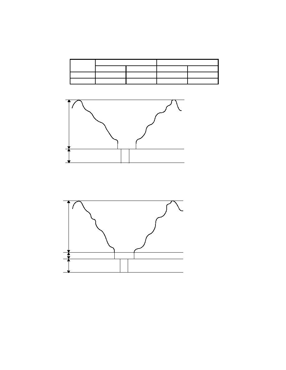
2�36
Table 2�18. K1 and K2 Values Defined
PEDESTAL
IOG
IOR, IOB
PEDESTAL
8-BIT OUTPUT
6-BIT OUTPUT
8-BIT OUTPUT
6-BIT OUTPUT
7.5 IRE
K1 = 11,294
K1 = 11,206
K2 = 8,067
K2 = 7,979
0 IRE
K1 = 10,684
K1 =10,600
K2 = 7,462
K2 = 7,374
White
Black/
Blank
Sync
100 IRE
40 IRE
[mA]
25.24
7.62
0.00
[V]
0.950
0.286
0.000
[mA]
17.62
0.00
[V]
0.660
0.000
Green
Red/Blue
NOTE A: 75-
doubly terminated load, Vref = 1.235 V, RSET = 523
. RS343A-levels and tolerances are assumed
on all levels.
Figure 2�14. Composite Video Output (With 0 IRE, 8-Bit Output)
White
Black
Blank
Sync
92.5 IRE
[mA]
26.67
9.05
7.62
0.00
[V]
1.000
0.340
0.286
0.000
[mA]
19.05
1.44
0.00
[V]
0.714
0.054
0.000
Green
Red/Blue
7.5 IRE
40 IRE
NOTE A: 75-
doubly terminated load, Vref = 1.235 V, RSET = 523
. RS343A-levels and tolerances are assumed on
all levels.
Figure 2�15. Composite Video Output (With 7.5 IRE, 8-Bit Output)
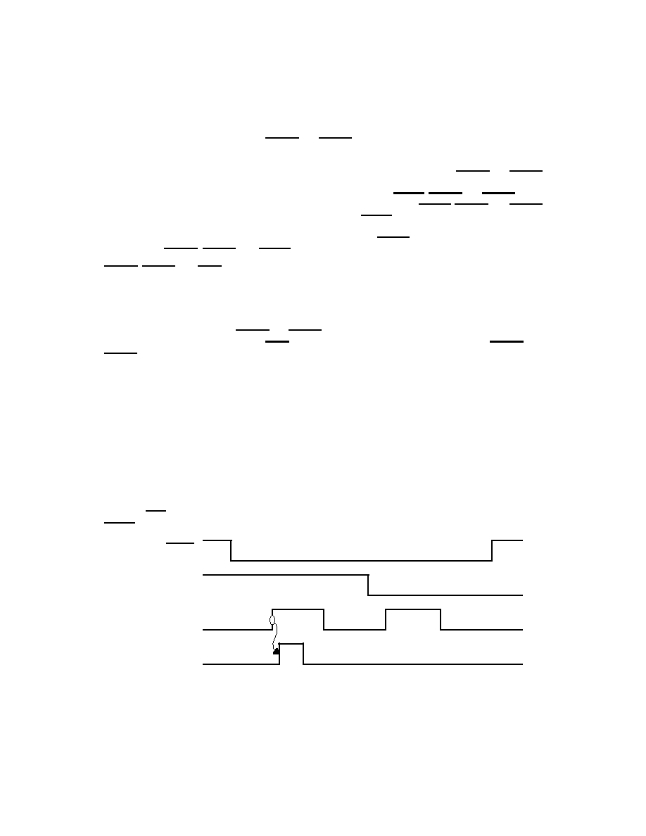
2�37
2.14 Video Control: Horizontal Sync, Vertical Sync, and Blank
For the high-resolution system modes, HSYNC and VSYNC are active-low pulses that are passed through
true/complement gates to the HSYNCOUT and VSYNCOUT outputs. The output polarities of HSYNCOUT
and VSYNCOUT can be programmed through the general control register. However, for the VGA mode, the
polarities required by the monitor are already provided at the feature connector where HSYNC and VSYNC
are sourced. Therefore, the palette passes them through to HSYNCOUT and VSYNCOUT without polarity
change. As described in Section 2.3 and Figures 2�2 through 2�5, the SYSBL, HSYNC and VSYNC inputs
are sampled and latched at the falling edge of VCLK in the system mode while VGABL, HSYNC, and VSYNC
are latched at the rising edge of CLK0 in the VGA mode. After SYSBL is sampled with VCLK, it is sampled
on the rising edge of the internal RCLK and passed to the dot-clock pipeline delay. When multiplexer control
register 2 bit 7 is set to 1 to activate the VGA port, the CLK0 and VGABL inputs are selected. Otherwise,
VCLK latches HSYNC, VSYNC, and SYSBL are selected.
HSYNC, VSYNC, and Blank (generated either from the system mode or VGA-mode video-control signals)
have internal pipeline delays so that the Sync and Blank signals align with the RGB data at the DAC outputs.
Due to the sample and latch-timing delay, it is possible to have active SCLKs after the selected blank input
becomes active. The relationship between VCLK and SCLK and the internal VCLK sample and latch delay
needs to be carefully reviewed and programmed (see Section 2.3
and Figures 2�2 and 2�3 for more details).
As shown in Figure 2�13, active HSYNC and VSYNC turns off the sync current source (after pipeline delay).
They are not qualified by the internal Blank signal. Therefore, to ensure proper operation, HSYNC and
VSYNC should be designed such that they are active only during Blank active time.
To alter the polarity of the HSYNCOUT and VSYNCOUT outputs, the MPU must set or clear the
corresponding bits in the general control register (see subsection 2.16.2). The polarity of these signals can
only be altered when not in VGA mode. These bits default to 0, which is an active-low output.
2.15 Split Shift Register Transfer VRAMs
Both the TVP3010C and the TVP3010M palettes have direct support for split-shift register transfer (SSRT)
VRAMs. In order to allow the VRAMs to perform a split-shift register transfer, an extra SCLK cycle must be
inserted during the Blank sequence. This is initiated when the SSRT enable bit 2 in the general control
register is set to 1 and a rising edge on the SFLAG input is detected. An SCLK pulse is generated within
20 ns of the rising edge of the SFLAG signal. A minimum 15-ns logic-high duration is provided to satisfy all
the � 15 VRAM timing requirements. The rising edge of the SFLAG input triggers SCLK, but it needs to stay
high for a specified minimum duration. By controlling the SFLAG timing, the delay time from the rising edge
of VRAM TRG signal to SCLK can be satisfied. The relationship between SCLK, the SFLAG input, and
SYSBL is shown as follows:
SYSBL
SSRT Enable
(general-control
register-bit 2)
SFLAG Input
SCLK
Figure 2�16. Split Shift Register Transfer Timing
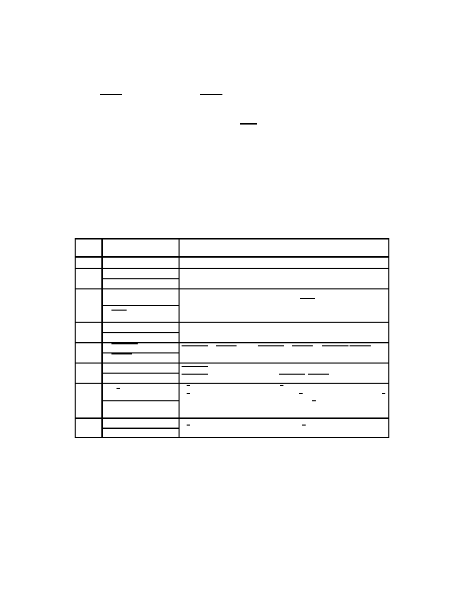
2�38
When external SFLAG logic is designed as an R � S latch that is set by split shift register transfer timing and
reset by SYSBL going high, the delay from SYSBL high to SFLAG low cannot exceed one-half of one SCLK
cycle. Otherwise, the SCLK generation logic could fail.
When the SSRT function is enabled but SFLAG is held low, the SCLK runs as if the SSRT function is
disabled. Since the SFLAG input is not qualified by the Blank signal within the palette, it needs to be held
low or disabled any time the SSRT SCLK pulse is not intended (see Section 2.3 and Figures 2�2 through
2�5 for more system details).
2.16 Control Register Definitions
The following paragraphs describe the operation of the TVP3010 control register.
2.16.1
Configuration Register
The configuration register (see Table 2�19) controls the dual-function terminals on the TVP3010C or
TVP3010M to maintain pin compatibility with the TLC3407x VIP parts. At reset, the configuration register
defaults to TLC3407x compatible-pin settings. Bit 7 of the configuration register corresponds to data-bus
bit 7, index = 1E (hex).
Table 2�19. Configuration Register
BIT
NAME
VALUES
DESCRIPTION
CR7
X
Reserved undefined
CR7
X
Reserved, undefined
CR6
0: In phase (default)
VCLK polarity select specifies whether the VCLK signal is in phase or opposite
CR6
1: Opposite phase
y
g
phase of the RCLK and SCLK signals.
CR5
0: Internal RCLK (default)
LCLK source selects the LCLK source. When bit 5 = 0, (default) LCLK is
internally connected to RCLK. When bit 5 = 1, CLK4[LCLK] is configured as the
CR5
1: CLK4[LCLK]
y
,
[
]
g
LCLK input and an external LCLK source must be supplied (see
subsection 2.3.1).
CR4
0: Disabled (default)
RCLK enable specifies whether RCLK is output on CLK3[RCLK]. When RCLK
CR4
1: Enabled
[
]
is disabled, then CLK3[RCLK] is CLK3 (see Section 2.3)
.
CR3
0: MUXOUT (default)
MUXOUT or SENSE selects MUXOUT or SENSE on MUXOUT[SENSE] (see
CR3
1: SENSE
MUXOUT or SENSE selects MUXOUT or SENSE on MUXOUT[SENSE] (see
Sections 2.9 and 2.10)
.
CR2
0: Low (default)
MUXOUT level terminal. When configuration register-bit CR3 = 0, then
CR2
1: High
MUXOUT level terminal. When configuration register bit CR3 0, then
MUXOUT controls the logic level on MUXOUT [SENSE].
CR1
0: 8/6 (default)
8/6 or OVS defines the terminal as 8/6 or OVS and controls the source of the
8/6 function signal. When CR1 = 0, then 8/6[OVS] is configured as the 8/6
CR1
1: OVS
g
,
[
]
g
terminal. When CR1 = 1, then CR0 controls the 8/6 function and is configured
as OVS (see Sections 2.1 and 2.7).
CR0
0: 6-bit (default)
8/6 level When CR1
1 CR0 controls the 8/6 operation (see Section 2 1)
CR0
1: 8-bit (high)
8/6 level. When CR1 = 1, CR0 controls the 8/6 operation (see Section 2.1)
.

2�39
2.16.2
General Control Register
The general control register, see Table 2�20, controls various functions of the VIP. This register can be
accessed by the MPU at any time. Bit 7 of the general control register corresponds to data bus bit 7,
index = 1D (hex).
Table 2�20. General Control Register
BIT
NAME
VALUES
DESCRIPTION
GCR7
0: External OVS terminal
(default)
Overscan-control select. GCR7 selects external terminal control or
internally-generated overscan control (see Section 2 7)
1: Internal
internally-generated overscan control (see Section 2.7).
GCR6
0: Disable (default)
Overscan enable. GCR6 specifies whether to enable the user-defined
GCR6
1: Enable
overscan-screen borders.
GCR5
0: Disable
Sync enable. GCR5 specifies whether Sync information is to be output onto
GCR5
1: Enable (default)
y
y
IOG.
GCR4
0: 0 IRE (default)
Pedestal control. GCR4 specifies whether a 0- or 7.5-IRE blanking pedestal is
to be generated on the video outputs 0 IRE specifies that the black and blank
GCR4
1: 7.5 IRE
to be generated on the video outputs. 0 IRE specifies that the black and blank
levels are the same.
GCR3
0: Little-endian (default)
Little-endian/big-endian select. GCR3 selects either little- or big-endian format
GCR3
1: Big-endian
g
g
for the pixel-bus frame-buffer interface (see Sections 2.4
and Appendix C).
GCR2
0: Disable (default)
Split shift register transfer enable (see Section 2 15)
GCR2
1: Enable
Split shift register transfer enable (see Section 2.15).
GCR1
0: Active (low) (default)
VSYNCOUT output polarity (see Section 2 14)
GCR1
1: Active (high)
VSYNCOUT output polarity (see Section 2.14).
GCR0
0: Active (low) (default)
HSYNCOUT output polarity (see Section 2 14)
GCR0
1: Active (high)
HSYNCOUT output polarity (see Section 2.14).
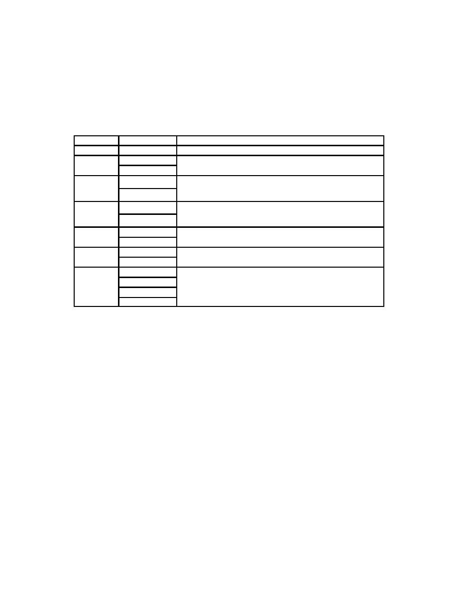
2�40
2.16.3
Cursor Control Register
The cursor control register, see Table 2�21, controls various on-chip cursor functions of the palette. This
register may be accessed by the MPU at any time. Bit 7 of the cursor control register corresponds to data
bus bit 7, index = 06 (hex).
Table 2�21. Cursor Control Register
BIT NAME
VALUES
DESCRIPTION
CCR7
X
Reserved
CCR6
0: Disable (default)
Sprite-cursor enable. CCR6 enables (1) or disables (0) the 64
�
64 sprite
CCR6
1: Enable
( )
( )
cursor.
CCR5
0: (default)
Dual-cursor format. CCR5 specifies the display format at the intersection of the
crosshair cursor and the user-defined cursor area (see subsection 2 5 5 and
CCR5
1:
crosshair cursor and the user-defined cursor area (see subsection 2.5.5, and
the cursor-intersection truth table).
CCR4
0: XGA (default)
64
�
64 cursor-mode select. CCR4 specifies whether the XGA (0) or
X-windows format is used to interpret the data stored in the 64
�
64 cursor
CCR4
1: X-windows
X-windows format is used to interpret the data stored in the 64
�
64 cursor
sprite RAM (see subsection 2.5.2)
.
CCR3
0: Color 0 (default)
Crosshair-color selection. CCR3 specifies whether the crosshair cursor is to
CCR3
1: Color 1
be displayed in color 1 (logical 1) or color 0 (logical 0).
CCR2
0: Disable (default)
Crosshair-cursor enable. CCR2 specifies whether the crosshair cursor is to be
CCR2
1: Enable
displayed in color 1 or not in color 0.
00: 1 pixel (default)
Crosshair thickness CRR1 and CCR0 specify whether the vertical and
CCR1 CCR0
01: 3 pixels
Crosshair thickness. CRR1 and CCR0 s ecify whether the vertical and
horizontal thickness of the crosshair is one, three, five, or seven pixels. The
CCR1, CCR0
10: 5 pixels
segments are centered about the value in the cursor-position (X and Y)
register
11: 7 pixels
register.
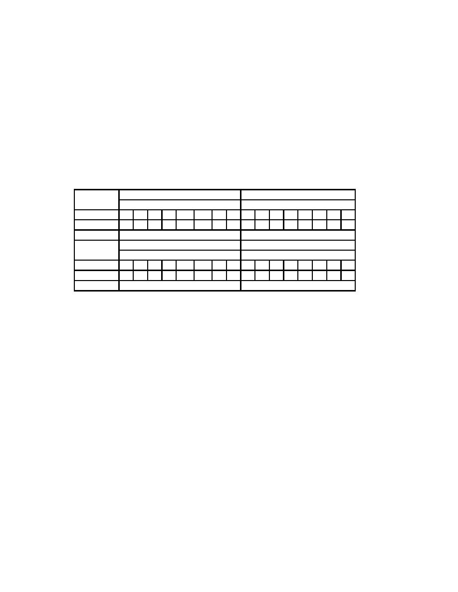
2�41
2.16.4
Cursor Position X and Y Registers
The cursor position X and Y registers specify the (X and Y) coordinate of the intersection of the crosshair
cursor. They are also used in conjunction with the sprite origin register to specify the location of the 64
�
64
cursor area (see subsection 2.5.3). The cursor position X register is made up of the cursor position X LSB
(CPXL) and the cursor position X MSB (CPXM); the cursor position Y register is made up of the cursor
position Y LSB (CPYL) and the cursor position Y MSB (CPYM). All registers are initialized to 00 (hex) and
can be written to or read from by the MPU at any time. The cursor position is not updated until the vertical
retrace interval after CPYM has been written to by the MPU.
CPXL and CPXM are cascaded to form a 12-bit cursor-position X register. Similarly, CPYL and CPYM are
cascaded to form a 12-bit cursor-position Y register. Bits D4 � D7 of CPXM and CPYM are always a zero.
Table 2�22. Cursor Position X and Y Registers
CURSOR POSITION X MSB
CURSOR POSITION X LSB
(CPXM)
(CPXL)
Data Bit
D7
D6
D5
D4
D3
D2
D1
D0
D7
D6
D5
D4
D3
D2
D1
D0
X Position
0
0
0
0
X11
X10
X9
X8
X7
X6
X5
X4
X3
X2
X1
X0
Index = 01h
Index = 00h
CURSOR POSITION Y MSB
CURSOR POSITION Y LSB
(CPYM)
(CPYL)
Data Bit
D7
D6
D5
D4
D3
D2
D1
D0
D7
D6
D5
D4
D3
D2
D1
D0
Y Position
0
0
0
0
Y11
Y10
Y9
Y8
Y7
Y6
Y5
Y4
Y3
Y2
Y1
Y0
Index = 03h
Index = 02h
The cursor position x value to be written is calculated as follows:
Cx = desired display screen X position
Values from 0000 (hex) to 0fff (hex) may be written into the cursor-position X register.
The cursor position Y value to be written is calculated as follows:
Cy = desired display screen Y position
Values from 0000 (hex) to 0fff (hex) may be written into the cursor position Y register.
The values written into the cursor position X and Y registers should be relative to the first displayed pixel
on the screen (i.e., 0,0).

2�42
2.16.5
Sprite Origin X and Y Registers
These registers are used to specify the (X and Y) location of the 64 x 64 sprite with respect to the crosshair
location (see subsection 2.5.3). The sprite origin X and Y registers can contain values from 0 to 63 decimal.
Both registers are initialized to 1F (hex), 31 (decimal), which sets the center of the crosshair at the center
of the 64
�
64 sprite. Both registers may be written to or read from by the MPU at any time. The sprite origin
is not updated until the vertical-retrace interval after sprite origin X and Y registers have been written by the
MPU.
Table 2�23. Sprite Origin X and Y Registers
SPRITE ORIGIN X
Data Bit
D7
D6
D5
D4
D3
D2
D1
D0
X Origin
0
0
X5
X4
X3
X2
X1
X0
Index = 04h
SPRITE ORIGIN Y
Data Bit
D7
D6
D5
D4
D3
D2
D1
D0
Y Origin
0
0
Y5
Y4
Y3
Y2
Y1
Y0
Index = 05h
Values from 00 (hex) to 3F (hex) may be written into the sprite origin X and Y registers. Bits D6 and D7 are
always cleared to 0.

2�43
2.16.6
Window Start X and Y Registers
These registers are used to specify the (X and Y) coordinate of the upper left corner of the crosshair-cursor
window or auxiliary window. As shown in Table 2�24, the window start X register is made up of the window
start X LSB (WSXL) and the window start X MSB (WSXM); the window start Y register is made up of the
window start Y LSB (WSYL) and the window start Y MSB (WSYM). They are not initialized and may be
written to or read from by the MPU at any time. The window start is not updated until the vertical-retrace
interval after WSYM has been written to by the MPU.
WSXL and WSXM are cascaded to form a 12-bit window start X register. Similarly, WSYL and WSYM are
cascaded to form a 12-bit window start Y register. Bits D4 � D7 of WSXM and WSYM are always set to 0.
Table 2�24. Window Start X and Y Registers
WINDOW START X MSB
WINDOW START X LSB
(WSXM)
(WSXL)
Data Bit
D7
D6
D5
D4
D3
D2
D1
D0
D7
D6
D5
D4
D3
D2
D1
D0
X Coordinate
0
0
0
0
X11
X10
X9
X8
X7
X6
X5
X4
X3
X2
X1
X0
Index = 11h
Index = 10h
WINDOW START Y MSB
WINDOW START Y LSB
(WSYM)
(WSYL)
Data Bit
D7
D6
D5
D4
D3
D2
D1
D0
D7
D6
D5
D4
D3
D2
D1
D0
Y Coordinate
0
0
0
0
Y11
Y10
Y9
Y8
Y7
Y6
Y5
Y4
Y3
Y2
Y1
Y0
Index = 15h
Index = 14h
The window start X value to be written is calculated as follows:
Wx = desired display screen X position
Values from 0000 (hex) to 0fff (hex) may be written into the window start X register.
The window start Y value to be written is calculated as follows:
Wy = desired display screen Y position
Values from 0000 (hex) to 0fff (hex) may be written into the window start Y register.
The values written into the window start X and Y registers should be relative to the first displayed pixel on
the screen (i.e., 0,0).
The window start location specified is the first location inside the window. For the crosshair cursor or auxiliary
window to be displayed, the window start registers must specify a point on the active display.
2�44
2.16.7
Window Stop X and Y Registers
These registers are used to specify the (X and Y) coordinate of the lower right corner of the crosshair cursor
or auxiliary window. As shown in Table 2�25, the window stop X register is made up of the window stop X
LSB (WSPXL) and the window stop X MSB (WSPXM); the window stop Y register is made up of the window
stop Y LSB (WSPYL) and the window stop Y MSB (WSPYM). They are not initialized and may be written
to or read from by the MPU at any time. The window stop is not updated until the vertical retrace interval
after WSPYM has been written to by the MPU.
WSPXL and WSPXM registers are cascaded to form a 12-bit window stop X register. Similarly, WSPYL and
WSPYM registers are cascaded to form a 12-bit window stop Y register. Bits D4 � D7 of WSPXM and
WSPYM are always cleared to 0.
Table 2�25. Window Stop X and Y Registers
WINDOW STOP X MSB
WINDOW STOP X LSB
(WSPXM)
(WSPXL)
Data Bit
D7
D6
D5
D4
D3
D2
D1
D0
D7
D6
D5
D4
D3
D2
D1
D0
X Coordinate
0
0
0
0
X11
X10
X9
X8
X7
X6
X5
X4
X3
X2
X1
X0
Index = 13h
Index = 12h
WINDOW STOP Y MSB
WINDOW STOP Y LSB
(WSPYM)
(WSPYL)
Data Bit
D7
D6
D5
D4
D3
D2
D1
D0
D7
D6
D5
D4
D3
D2
D1
D0
Y Coordinate
0
0
0
0
Y11
Y10
Y9
Y8
Y7
Y6
Y5
Y4
Y3
Y2
Y1
Y0
Index = 17h
Index = 16h
The window stop X value to be written is calculated as follows:
Wx = desired display screen X position
Values from 0000 (hex) to 0fff (hex) may be written into the window stop X register.
The window stop Y value to be written is calculated as follows:
Wy = desired display screen Y position
Values from 0000 (hex) to 0fff (hex) may be written into the window stop Y register.
The values written into the window stop X and Y registers should be relative to the first displayed pixel on
the screen (i.e., 0,0).
The window stop location specified is the last location inside the window. For the crosshair cursor or auxiliary
window to be displayed, the window start registers must specify a point on the active display.

2�45
2.16.8
Cursor Color 0, 1 RGB Registers
These registers are used to specify the two colors for the hardware cursor (see Section 2.5). They are not
initialized and may be written to or read from by the MPU at any time. Note that there are six registers total,
three for each color. The register format for both the cursor-color 0 and cursor color 1 registers is shown
in Table 2�26.
Table 2�26. Cursor Color RGB Registers
CURSOR COLOR RED
Data Bit
D7
D6
D5
D4
D3
D2
D1
D0
Red Value
R7
R6
R5
R4
R3
R2
R1
R0
Index = 23h and 26h
CURSOR COLOR GREEN
Data Bit
D7
D6
D5
D4
D3
D2
D1
D0
Green Value
G7
G6
G5
G4
G3
G2
G1
G0
Index = 24h and 27h
CURSOR COLOR BLUE
Data Bit
D7
D6
D5
D4
D3
D2
D1
D0
Blue Value
B7
B6
B5
B4
B3
B2
B1
B0
Index = 25h and 28h
Values 00 (hex) to FF (hex) may be written into the cursor color registers.

2�46
2.16.9
Cursor RAM Address Register
These registers are used to specify the address of where to write or read sprite cursor data from. The linear
addressing scheme is depicted in Figure 2 � 6 of subsection 2.5.1. As shown in Table 2�27, the cursor RAM
register is made up of the cursor-RAM address LSB (CRAL) and the cursor RAM address MSB (CRAM).
They are not initialized and may be written to by the MPU at any time.
CRAL and CRAM are cascaded to form a 10-bit cursor-RAM address register. Bits D2 � D7 of CRAM are
always cleared to 0.
Table 2�27. Cursor RAM Address Register
CURSOR RAM ADDRESS MSB
CURSOR RAM ADDRESS LSB
(CRAM)
(CRAL)
Data Bit
D7
D6
D5
D4
D3
D2
D1
D0
D7
D6
D5
D4
D3
D2
D1
D0
Address
0
0
0
0
0
0
A9
A8
A7
A6
A5
A4
A3
A2
A1
A0
Index = 09h
Index = 08h
Values from 0000 (hex) to 03FF (hex) may be written into the cursor-RAM address register. When the
cursor-RAM address is to be written, both registers must be written with the cursor-RAM address LSB being
the first.
2.16.10 Cursor RAM Data Register
This register is used to read and write the contents of the sprite-cursor locations whose address is specified
in the cursor-RAM address registers. The data read from or written to this register contain four pixels of
information and two bit-planes per cursor pixel (see Figure 2 � 6 and subsection 2.5.1). The register is not
initialized and may be written to or read from by the MPU at any time. The sprite-cursor data format is shown
in Table 2-28.
Table 2�28. Cursor RAM Data Register
CURSOR-RAM DATA
Data Bit
D7
D6
D5
D4
D3
D2
D1
D0
Data
P13
P03
P12
P02
P11
P01
P10
P00
Index = 0Ah
Values from 00 (hex) to FF (hex) may be written into the cursor RAM data register.
2�47
2.16.11 Auxiliary-Control Register
The auxiliary-control register (see Table 2�29) is used to control various functions of the TVP3010C and
TVP3010M palettes including the auxiliary-windowing function and horizontal zooming. It can be accessed
by the MPU at any time. Bit 7 of the auxiliary-control register corresponds to data-bus bit 7, index = 29 (hex).
Table 2�29. Auxiliary-Control Register
BIT NAME
VALUES
DESCRIPTION
ACR7
0: (default)
Horizontal zoom control (see Section 2 8)
ACR7
1:
Horizontal zoom control (see Section 2.8)
.
ACR6
0: (default)
Horizontal zoom control (see Section 2 8)
ACR6
1:
Horizontal zoom control (see Section 2.8)
.
ACR5
0: (default)
Horizontal zoom control (see Section 2 8
)
ACR5
1:
Horizontal zoom control (see Section 2.8
).
ACR4
X
Reserved
ACR3
0: Externally clocked
Frame-buffer clocking select. ACR3 selects self-clocked or externally
ACR3
1: Self clocked (default)
g
y
clocked timing for the pixel-port (P0 � P63) (see subsection 2.3.2).
ACR2
0: PSEL disable (default)
Windowing-function select. ACR2 is a port-select enable (see equation
ACR2
1: PSEL enable
g
(
q
(1) in subsection 2.6.1)
.
ACR1
0: Window disable (default)
Windowing-function select. ACR1 is an auxiliary-window enable (see
ACR1
1: Window enable
g
y
(
equation (1) in subsection 2.6.1)
.
ACR0
0: True function
Windowing-function select. ACR0 is a complementary-function bit (see
ACR0
1: Complement (default)
g
y
(
equation (1) in subsection 2.6.1)
.
2�48
2.16.12 Color-Key Control Register
The color-key control register (see Table 2�30) controls the operation of the color-key switching function
(see subsection 2.6.2). It can be accessed by the MPU at any time. Bit 7 of the color-key control register
corresponds to data-bus bit 7, index = 38 (hex).
Table 2�30. Color-Key Control Register
BIT NAME
VALUES
DESCRIPTION
CKC7
X
Reserved
CKC6
X
Reserved
CKC5
X
Reserved
0: True function
Color key function select CKC4 is a complementary function bit (see
CKC4
1: Complement
(default)
Color-key function select. CKC4 is a complementary function bit (see
equation 2 in subsection 2.6.2).
CKC3
0: Disable compare
(default)
Blue-compare enable. CKC3 enables or disable the direct-color blue field
comparison (see equation 2 in subsection 2 6 2)
1: Enable comparison
comparison (see equation 2 in subsection 2.6.2)
.
CKC2
0: Disable compare
(default)
Green-compare enable. CKC2 enables or disables the direct-color
green-field comparison (see equation 2 in subsection 2 6 2)
1: Enable comparison
green-field comparison (see equation 2 in subsection 2.6.2)
.
CKC1
0: Disable compare
(default)
Red-compare enable. CKC1 enables or disables the direct-color red-field
comparison (see equation 2 in subsection 2 6 2)
1: Enable comparison
comparison (see equation 2 in subsection 2.6.2).
CKC0
0: Disable compare
(default)
Overlay/VGA-compare enable. CLC0 enables or disables the direct-color
overlay-/VGA-field comparison (see equation 2 in subsection 2 6 2)
1: Enable comparison
overlay-/VGA-field comparison (see equation 2 in subsection 2.6.2).
2�49
2.16.13 Color-Key (Red, Green, Blue, Overlay) Low and High Registers
These registers are used to specify the color-comparison ranges for the four direct-color data fields when
performing color-key switching. A low and a high register are provided for each of the four data fields to
facilitate the range comparison (see Section 2.6 and subsection 2.6.2 for more details on their usage). All
four low registers are initialized with 01 (hex), while all four high registers are initialized with FF (hex). The
registers may be written to or read from by the MPU at any time. There are eight registers total, two for each
color. The register formats for both low and high registers are shown in Table 2�31.
Table 2�31. Color-Key Low and High Registers
COLOR-KEY LOW
Data Bit
D7
D6
D5
D4
D3
D2
D1
D0
Low Value
L7
L6
L5
L4
L3
L2
L1
L0
Index = 30h, 32h, 34h, and 36h
COLOR-KEY HIGH
Data Bit
D7
D6
D5
D4
D3
D2
D1
D0
High Value
H7
H6
H5
H4
H3
H2
H1
H0
Index = 31h, 33h, 35h, and 37h
Values 00 (hex) to FF (hex) may be written into the four color-key low and four color-key high registers.
2�50
2.16.14 Overscan-Color RGB Registers
The overscan-color RGB registers specify the color for the overscan function. This function can be used to
create custom-overscan screen borders (see Section 2.7). They are not initialized and may be written to
or read from by the MPU at any time. The register formats for the overscan-color RGB registers are shown
in Table 2�32.
Table 2�32. Overscan-Color RGB Register
OVERSCAN-COLOR RED
Data Bit
D7
D6
D5
D4
D3
D2
D1
D0
Red Value
R7
R6
R5
R4
R3
R2
R1
R0
Index = 20h
OVERSCAN-COLOR GREEN
Data Bit
D7
D6
D5
D4
D3
D2
D1
D0
Green Value
G7
G6
G5
G4
G3
G2
G1
G0
Index = 21h
OVERSCAN-COLOR BLUE
Data Bit
D7
D6
D5
D4
D3
D2
D1
D0
Blue Value
B7
B6
B5
B4
B3
B2
B1
B0
Index = 22h
Values 00 (hex) to FF (hex) may be written into the overscan-color RGB registers.
2�51
2.16.15 CRC LSB and MSB Registers
The CRC LSB and MSB registers (Table 2�33) are used to read the result of the 16-bit CRC calculation (see
subsection 2.9.1). These registers are not initialized and may be read from by the MPU at any time. Note,
however, that they are only updated on the rising edge of the second HSYNC during vertical retrace.
CRCLSB and CRCMSB are cascaded to form a 16-bit CRC-calculation remainder.
Table 2�33. CRC MSB and LSB Registers
CRC MSB
CRC LSB
Data Bit
D7
D6
D5
D4
D3
D2
D1
D0
D7
D6
D5
D4
D3
D2
D1
D0
CRC Remainder
R15
R14
R13
R12
R11
R10
R9
R8
R7
R6
R5
R4
R3
R2
R1
R0
Index = 3Dh
Index = 3Ch
2.16.16 CRC Control Register
The CRC control register is a write-only register used to specify on which of the 24 DAC-data lines the 16-bit
CRC should be calculated (see subsection 2.9.1). This register is not initialized and may be written to by
the MPU at any time. The CRC control register data format is shown in Table 2�34.
Table 2�34. CRC Control Register Format
CRC CONTROL REGISTER
Data Bit
D7
D6
D5
D4
D3
D2
D1
D0
Select Data
0
0
0
D4
D3
D2
D1
D0
Index = 3Eh
Values from 00 (hex) to 17 (hex) may be written into the CRC control register.
3�1
3 Electrical Characteristics
3.1
Absolute Maximum Ratings Over Operating Free-Air Temperature Range
(unless otherwise noted)
Supply voltage, AV
DD,
DV
DD
(see Note 1)
7 V
. . . . . . . . . . . . . . . . . . . . . . . . . . . . . . . . . . .
Input voltage range, V
I
� 0.5 V to V
DD
+ 0.5 V
. . . . . . . . . . . . . . . . . . . . . . . . . . . . . . . . . . .
Analog output short-circuit duration to any power supply or common
unlimited
. . . . . . .
Operating free-air temperature range, T
A
: TVP3010C
0
_
C to 70
_
C
. . . . . . . . . . . . . . . .
TVP3010M
�55
_
C to 125
_
C
. . . . . . . . . . . .
Storage temperature range, T
stg
� 65
_
C to 150
_
C
. . . . . . . . . . . . . . . . . . . . . . . . . . . . . . . .
Virtual Junction temperature, T
J
175
�
C
. . . . . . . . . . . . . . . . . . . . . . . . . . . . . . . . . . . . . . . . . .
Case temperature for 10 seconds, T
C
: FN and GA package
260
�
C
. . . . . . . . . . . . . . . . .
Lead temperature 1,6 mm (1/16 inch) from case for 10 seconds
260
�
C
. . . . . . . . . . . . . .
Stresses beyond those listed under "absolute maximum ratings" may cause permanent damage to the device. These
are stress ratings only, and functional operation of the device at these or any other conditions beyond those indicated
under "recommended operating conditions" is not implied. Exposure to absolute-maximum-rated conditions for
extended periods may affect device reliability.
NOTE 1: All voltage values are with respect to GND.
3.2
Recommended Operating Conditions
MIN
NOM
MAX
UNIT
Supply voltages, AVDD, DVDD
4.75
5
5.25
V
Reference voltage V f
TVP3010C
1.15
1.235
1.26
V
Reference voltage, Vref
TVP3010M
1.1
1.235
1.3
V
High-level input voltage, VIH
2.4
VDD+0.5
V
Low-level input voltage, VIL
0.8
V
Differential voltage on ECL inputs, VID
0.6
6
V
Common-mode input voltage on ECL inputs, VIC
2.85
3.15
VDD � 0.5
V
Output load resistance, RL
37.5
FS ADJUST resistor, RSET
523
Operating free-air temperature TA
TVP3010C
0
70
�
C
O erating free-air tem erature, TA
TVP3010M
� 55
125
�
C
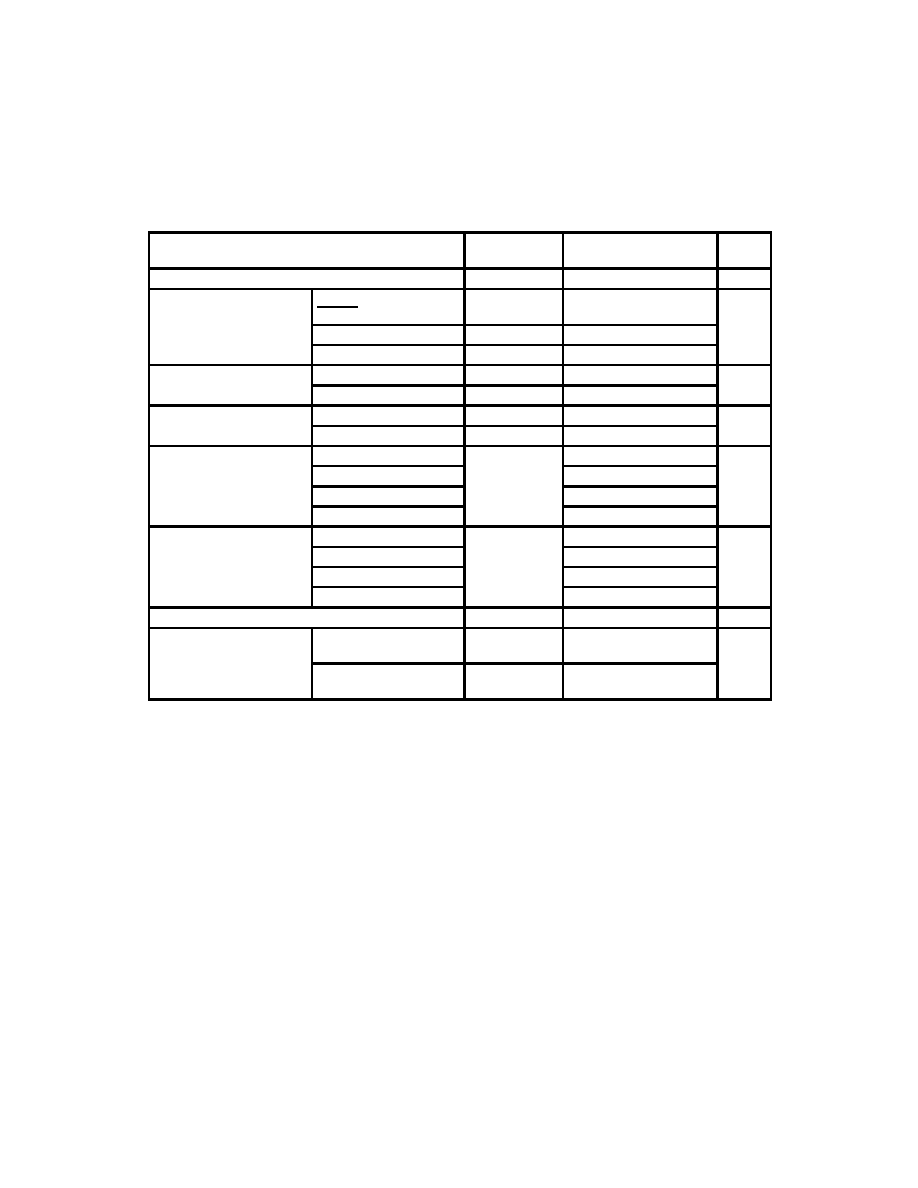
3�2
3.3 Electrical Characteristics for TVP3010C Over Recommended Ranges of
Supply Voltage and Operating Free-Air Temperature (Unless Otherwise
Noted)
PARAMETER
TEST
CONDITIONS
MIN
TYP
MAX
UNIT
VOH
High-level output voltage
IOH = � 800
�
A
2.4
V
V
Low-level output
D(0 � 7), VCLK, RCLK,
SENSE
IOL = 3.2 mA
0.4
V
VOL
Low level out ut
voltage
HSYNCOUT, VSYNCOUT
IOL = 15 mA
0.4
V
SCLK
IOL = 18 mA
0.4
IIH
High-level input
TTL inputs
VI = 2.4 V
1
�
A
IIH
g
current
ECL inputs
VI = 4 V
1
�
A
IIL
Low-level input
TTL inputs
VI = 0.8 V
�1
�
A
IIL
current
ECL inputs
VI = 0.4 V
�1
�
A
TVP3010-85
250
280
IDD
Supply current,
pseudo color mode
TVP3010-110
VDD = 5
270
320
mA
IDD
pseudo-color mode
(see Note 2)
TVP3010-135
VDD = 5
330
380
mA
(see Note 2)
TVP3010-170
390
440
TVP3010-85
270
320
IDD
Supply current, true-
TVP3010-110
VDD = 5
320
370
mA
IDD
y
,
color mode
TVP3010-135
VDD = 5
370
420
mA
TVP3010-170
420
475
IOZ
High-impedance-state output current
10
�
A
Ci
Input capacitance
TTL inputs
f = 1 MHz,
VI = 2.4 V
4
pF
Ci
Input capacitance
ECL inputs
f = 1 MHz,
VI = 4 V
4
pF
All typical values are at VDD = 5 V, TA = 25
�
C.
NOTE 2: IDD is measured with dot clock running at the maximum specified frequency, SCLK
frequency = dot-clock frequency/8 (in pseudo-color modes), and the palette RAM loaded with repeating
full-range toggling patterns (00h/00h/00h/00h/FFh/FFh/FFh/FFh). Pseudo-color mode is also known as
color-indexing mode.

3�3
3.4 Electrical Characteristics for TVP3010M Over Recommended Ranges of
Supply Voltage and Operating Free-Air Temperature (Unless Otherwise
Noted)
PARAMETER
TEST
CONDITIONS
MIN
TYP
MAX
UNIT
VOH
High-level output voltage
IOH = � 800
�
A
2.4
V
V
L
l
l
t
t
lt
D(0 � 7), VCLK, RCLK,
SENSE
IOL = 3.2 mA
0.4
V
VOL
Low-level output voltage
HSYNCOUT, VSYNCOUT
IOL = 15 mA
0.4
V
SCLK
IOL = 18 mA
0.4
IIH
High level input current
TTL inputs
VI = 2 V
10
�
A
IIH
High-level input current
ECL inputs
VI = 4 V
10
�
A
IIL
Low level input current
TTL inputs
VI = 0.8 V
�10
�
A
IIL
Low-level input current
ECL inputs
VI = 0.4 V
�10
�
A
IDD
Supply current,
pseudo-color mode (see
Note 2)
TVP3010-135M
VDD = 5,
See Note 3
330
550
mA
IDD
Supply current,
true-color mode
VDD = 5,
See Note 3
370
575
mA
IOZ
High-impedance-state output current
25
�
A
Ci
Input capacitance
TTL inputs
f = 1 MHz,
VI = 2.4 V
4
pF
Ci
Input capacitance
ECL inputs
f = 1 MHz,
VI = 4 V
4
pF
All typical values are at VDD = 5 V, TA = 25
�
C.
NOTES:
2. IDD is measured with dot clock running at the maximum specified frequency, SCLK
frequency = dot-clock frequency/8 (in pseudo-color modes), and the palette RAM loaded with repeating
full-range toggling patterns (00h/00h/00h/00h/FFh/FFh/FFh/FFh). Pseudo-color mode is also known as
color-indexing mode.
3. This is worst-case supply current. The outputs (IOR, IOG, and IOB) are switched between zero scale
(black) and full scale (white) on every clock cycle. Supply currents can be reduced by using more efficient
pixel clocking.

3�4
3.5 Operating Characteristics (TVP3010C) (see Note 4)
PARAMETER
TEST CONDITIONS
MIN
TYP
MAX
UNIT
Resolution (each DAC)
8/6 high
8
bits
Resolution (each DAC)
8/6 low
6
bits
EL
End-point linearity error
8/6 high
1
LSB
EL
y
(each DAC)
8/6 low
1/4
LSB
ED
Differential linearity error
8/6 high
1
LSB
ED
y
(each DAC)
8/6 low
1/4
LSB
Gray-scale error
5%
White level relative to Blank
17.69
19.05
20.4
mA
White level relative to Black
(7.5 IRE only)
16.74
17.62
18.5
mA
O
Black level relative to Blank
(7.5 IRE only)
0.95
1.44
1.9
mA
Output current (see Note 4)
Blank level on IOR, IOB
0
5
50
�
A
Blank level on IOG (with Sync enabled)
6.29
7.6
8.96
mA
Sync level on IOG (with Sync enabled)
0
5
50
�
A
One LSB (8/6 high)
69.1
�
A
One LSB (8/6 low)
276.4
�
A
DAC-to-DAC matching
2%
5%
DAC-to-DAC crosstalk
�20
dB
Output compliance
�1
1.2
V
Voltage reference output
voltage
1.15
1.235
1.26
V
Output impedance
50
k
Output capacitance
f = 1 MHz,
IOUT = 0
13
pF
Sense voltage reference
300
350
400
mV
Clock and data feedthrough
�20
dB
Glitch impulse (see Note 5)
50
pV�s
Pipeline delay VGA port
Self-clocked timing
18 dot clock
periods
Pipeline delay, VGA port
Externally clocked timing
15 dot clock
periods
Pipeline delay pixel port
Self-clocked timing
2 RCLK + 14 dot clock
periods
Pipeline delay, pixel port
Externally clocked timing
1 RCLK +14 dot clock
periods
NOTES:
4. Test conditions for RS343-A video signals (unless otherwise specified) can be found in Recommended
Operating Conditions using external voltage reference Vref = 1.235 V, RSET = 523
. When using the
internal voltage reference, RSET may need to be adjusted in order to meet these limits.
5. Glitch impulse does not include clock and data feedthrough. The � 3-dB test bandwidth is twice the clock
rate.
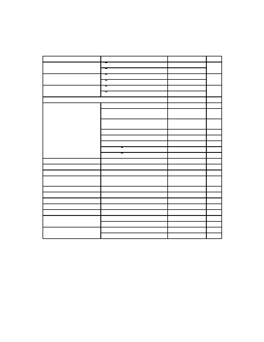
3�5
3.6 Operating Characteristics (TVP3010M)
PARAMETER
TEST CONDITIONS (see Note 4)
MIN
TYP
MAX
UNIT
Resolution (each DAC)
8/6 high
8
bits
Resolution (each DAC)
8/6 low
6
bits
EL
End-point linearity error
8/6 high
1
LSB
EL
y
(each DAC)
8/6 low
1/4
LSB
ED
Differential linearity error
8/6 high
1
LSB
ED
y
(each DAC)
8/6 low
1/4
LSB
Gray scale error
5%
White level relative to Blank
17.69
19.05
20.4
mA
White level relative to Blank
(7.5 IRE only)
16.74
17.62
18.5
mA
O
Black level relative to Blank
(7.5 IRE only)
0.95
1.44
1.9
mA
Output current (see Note 4)
Blank level on IOR, IOB
0
5
50
�
A
Blank level on IOG (with Sync enabled)
6.29
7.6
8.96
mA
Sync level on IOG (with Sync enabled)
0
5
50
�
A
One LSB (8/6 high)
69.1
�
A
One LSB (8/6 low)
276.4
�
A
DAC-to-DAC matching
2%
5%
DAC-to-DAC crosstalk
�20
dB
Output compliance
�0.4
1.2
V
Voltage reference output
voltage
1.1
1.235
1.3
V
Output impedance
50
k
Output capacitance
f = 1 MHz,
IOUT = 0
13
pF
Sense voltage reference
350
mV
Clock and data feedthrough
�20
dB
Glitch impulse (see Note 5)
50
pV�s
Pipeline delay VGA port
Self-clocked timing
18 dot clock
periods
Pipeline delay, VGA port
Externally clocked timing
15 dot clock
periods
Pipeline delay pixel port
Self-clocked timing
2 RCLK + 14 dot clock
periods
Pipeline delay, pixel port
Externally clocked timing
1 RCLK +14 dot clock
periods
NOTES:
4. Test conditions for RS343-A video signals (unless otherwise noted) can be found in Recommended
Operating Conditions using external voltage reference Vref = 1.235 V, RSET = 523
. When using the
internal voltage reference, RSET may need to be adjusted in order to meet these limits.
5. Glitch impulse does not include clock and data feedthrough. The � 3-dB test bandwidth is twice the clock
rate.

3�6
3.7 Timing Requirements (TVP3010C) (see Note 6)
TVP3010
-85
TVP3010
-110
TVP3010
-135
TVP3010
-170
UNIT
MIN
MAX
MIN
MAX
MIN
MAX
MIN
MAX
Dot clock frequency
85
110
135
170
MHz
CLK0 frequency for VGA
pass-through mode (see Note 7)
85
85
85
85
MHz
t
Clock cycle time
TTL
11.8
9.1
7.4
7.1
ns
tc
Clock cycle time
ECL
11.8
9.1
7.4
5.8
ns
tsu1
Setup time, RS(0 � 3) valid before RD
or WR
10
10
10
10
ns
th1
Hold time, RS(0 � 3) valid after RD or
WR
10
10
10
10
ns
tsu2 Setup time, D(0 � 7) valid before WR
35
35
35
35
ns
th2
Hold time, D(0 � 7) valid after WR
0
0
0
0
ns
tsu3
Setup time, VGA(0 � 7) and VGABL
valid before CLK0
(see Note 8)
2
2
2
2
ns
th3
Hold time, VGA(0 � 7) and VGABL
valid after CLK0
(see Note 8)
2
2
2
2
ns
tsu4
Setup time, P(0 � 31) and PSEL valid
before LCLK
(see Note 9)
2
2
2
2
ns
th4
Hold time, P(0 � 31) and PSEL valid
after LCLK
(see Note 9)
5
5
5
5
ns
tsu5
Setup time, HSYNC, VSYNC, and
SYSBL valid before VCLK
5
5
5
5
ns
th5
Hold time, HSYNC, VSYNC and
SYSBL valid after VCLK
1
1
1
1
ns
tw1
Pulse duration, RD or WR low
50
50
50
50
ns
tw2
Pulse duration, RD or WR high
30
30
30
30
ns
t 3
Pulse duration clock high
TTL
4
3.5
3
3
ns
tw3
Pulse duration, clock high
ECL
4
3
3
2.5
ns
t 4
Pulse duration clock low
TTL
4
3.5
3
3
ns
tw4
Pulse duration, clock low
ECL
4
3
3
2.5
ns
tw5
Pulse duration, SFLAG high
(see Note 10)
30
30
30
30
ns
tw6
Pulse duration, SCLK high
(see Note 10)
15
55
15
55
15
55
15
55
ns
NOTES:
6. TTL-input signals are 0 to 3 V with less than 3-ns rise/fall time between the 10% and 90% levels, unless
otherwise specified. ECL-input signals are VDD �1.8 V to VDD � 0.8 V with less than 2-ns rise/fall time
between the 20% and 80% levels. For input and output signals, timing reference points are at the 10% and
90% signal levels. Analog-output loads are less than 10 pF. D(0 � 7) output loads are less than 50 pF. All
other output loads are less than 50 pF, unless otherwise specified.
7. In VGA mode, CLK0 minimum pulse duration for clock low should be greater than 4.8 ns. When VGA
switching is to be performed using self-clocked timing, the maximum pixel rate cannot exceed 50 MHz.
8. Reference to CLK0 input only.
9. RCLK is delayed from SCLK in such a way that when RCLK is connected to LCLK, the timing is essentially
the same as the TLC3407x family of parts.
10. This parameter applies when the split shift-register transfer (SSRT) function is enabled (see Section 2.15
for details).

3�7
3.8 Timing Requirements (TVP3010M) (see Note 6)
MIN
MAX
UNIT
Dot clock frequency
135
MHz
CLK0 frequency for VGA pass-through mode (see Note 7)
85
MHz
t
Clock cycle time
TTL
7.4
ns
tc
Clock cycle time
ECL
7.4
ns
tsu1 Setup time, RS(0 � 3) valid before RD or WR
10
ns
th1
Hold time, RS(0 � 3) valid after RD or WR
10
ns
tsu2 Setup time, D(0 � 7) valid before WR
35
ns
th2
Hold time, D(0 � 7) valid after WR
0
ns
tsu3 Setup time, VGA(0 � 7) and VGABL valid before CLK0
(see Note 8)
2
ns
th3
Hold time, VGA(0 � 7) and VGABL valid after CLK0
(see Note 8)
2
ns
tsu4 Setup time, P(0 � 31) and PSEL valid before LCLK
(see Note 9)
2
ns
th4
Hold time, P(0 � 31) and PSEL valid after LCLK
(see Note 9)
5
ns
tsu5 Setup time, HSYNC, VSYNC, and SYSBL valid before VCLK
5
ns
th5
Hold time, HSYNC, VSYNC and SYSBL valid after VCLK
1
ns
tw1
Pulse duration, RD or WR low
50
ns
tw2
Pulse duration, RD or WR high
30
ns
t 3
Pulse duration clock high
TTL
3
ns
tw3
Pulse duration, clock high
ECL
3
ns
t 4
Pulse duration clock low
TTL
3
ns
tw4
Pulse duration, clock low
ECL
3
ns
tw5
Pulse duration, SFLAG high (see Note 10)
30
ns
tw6
Pulse duration, SCLK high (see Note 10)
15
55
ns
NOTES:
6. TTL-input signals are 0 to 3 V with less than 3-ns rise/fall time between the 10% and 90% levels, unless
otherwise specified. ECL input signals are VDD �1.8 V to VDD � 0.8 V with less than 2-ns rise/fall time
between the 20% and 80% levels. For input and output signals, timing reference points are at the 10% and
90% signal levels. Analog-output loads are less than 10 pF. D(0 � 7) output loads are less than 50 pF. All
other output loads are less than 50 pF, unless otherwise specified.
7. In VGA mode, CLK0 minimum pulse duration for clock low should be greater than 4.8 ns. When VGA
switching is to be performed using self-clocked timing, the maximum pixel rate cannot exceed 50 MHz.
8. Reference to CLK0 input only.
8. RCLK is delayed from SCLK in such a way that when RCLK is connected to LCLK, the timing is essentially
the same as the TLC3407x family of parts.
10. This parameter applies when the split shift-register transfer (SSRT) function is enabled (see Section 2.15
for details).

3�8
3.9 Switching Characteristics for TVP3010C Over Recommended Ranges of
Supply Voltage and Operating Free-Air Temperature (see Figures 3-1
to 3-3)
PARAMETER
TVP3010-85
TVP3010-110
UNIT
PARAMETER
MIN
TYP
MAX
MIN
TYP
MAX
UNIT
SCLK frequency (CL
15 pF) (see
Note 11)
85
85
MHz
SCLK frequency (CL
60 pF) (see
Note 11)
85
85
MHz
RCLK/VCLK frequency (see Note 11)
85
85
MHz
ten
Enable time, RD low to D(0 � 7) valid
40
40
ns
tdis
Disable time, RD high to D(0 � 7) disabled
17
17
ns
tv
Valid time, D(0 � 7) valid after RD high
5
5
ns
tPLH1
Propagation delay, SFLAG
to SCLK
high (see Notes 11 and 12)
0
20
0
20
ns
td1
Delay time, RD low to D(0 � 7) starting to
turn on
5
5
ns
td2
Delay time, selected input clock high/low
to dot clock (internal signal) high/low
7
7
ns
td3
Delay time, SCLK high/low to RCLK
high/low (see Note 13)
1
2
5
1
2
5
ns
td4
Delay time, VCLK high/low to RCLK
high/low (see Note 13)
1
3
6
1
3
6
ns
td5
Delay time, RCLK high/low from dot clock
high/low (internal signal)
7
7
ns
td6
Delay time, LCLK from RCLK
tRCLK�7
tRCLK�7
ns
td7
Delay time, dot clock high to
IOR/IOG/IOB active (analog output delay
time) (see Note 14)
4
4
ns
td8
Analog output settling time (see Note 15)
6
6
ns
td9
Delay time, dot clock high to HSYNCOUT
and VSYNCOUT valid
9
9
ns
tr
Analog output rise time (see Note 16)
2
2
ns
Analog output skew
0
2
0
2
ns
NOTES: 11. SCLK can drive an output capacitive load up to 60 pF. The worst-case transition time between the 10% and
90% levels is less than 4 ns (typical 3 ns). RCLK and VCLK can drive output capacitive loads up to 15 pF,
with worst-case transition times between 10% and 90% levels less than 4 ns (typical 3 ns).
12. This parameter applies when the split-shift register transfer (SSRT) function is enabled (see Section 2.15
for details).
13. The SCLK and VCLK delay time to RCLK depends on the load that the signals drive. This parameter is
measured with an RCLK to VCLK ratio of 1:1, a VCLK = RCLK load of 15 pF, and an SCLK load of 60 pF.
14. Measured from the 90% point of the rising edge of the internal dot-clock signal to 50% of the full-scale
transition
15. Measured from the 50% point of the full-scale transition to the point at which the output has settled within
�
1 LSB (settling time does not include clock and data feedthrough)
16. Measured between 10% and 90% of the full-scale transition
3�9
3.9 Switching Characteristics for TVP3010C Over Recommended Ranges of
Supply Voltage and Operating Free-Air Temperature (see Figures 3-1
to 3-3) (Continued)
PARAMETER
TVP3010C- 135
TVP3010C-170
UNIT
PARAMETER
MIN
TYP
MAX
MIN
TYP
MAX
UNIT
SCLK frequency (CL
15 pF)
(see Note 11)
85
87.5
MHz
SCLK frequency (CL
60 pF)
(see Note 11)
85
85
MHz
RCLK, VCLK frequency (see Note 11)
85
85
MHz
ten
Enable time, RD low to D(0 � 7) valid
40
40
ns
tdis
Disable time, RD high to D(0 � 7) disabled
17
17
ns
tv
Valid time, D(0 � 7) valid after RD high
5
5
ns
tPLH1
Propagation delay, SFLAG
to SCLK
high (see Notes 11 and 12)
0
20
0
20
ns
td1
Delay time, RD low to D(0 � 7) starting to
turn on
5
5
ns
td2
Delay time, selected input clock high/low
to dot clock (internal signal) high/low
7
7
ns
td3
Delay time, SCLK high/low to RCLK
high/low (see Note 13)
1
2
5
1
2
5
ns
td4
Delay time, VCLK high/low to RCLK
high/low (see Note 13)
1
3
6
1
3
6
ns
td5
Delay time, RCLK high/low from dot clock
high/low (internal signal)
7
7
ns
td6
Delay time, LCLK from RCLK
tRCLK�7
tRCLK�7
ns
td7
Delay time, dot clock high to
IOR/IOG/IOB active (analog output delay
time) (see Note 14)
4
4
ns
td8
Analog output settling time (see Note 15)
6
5
ns
td9
Delay time, dot clock high to HSYNCOUT
and VSYNCOUT valid
9
9
ns
tr
Analog output rise time (see Note 16)
2
2
ns
Analog output skew
0
2
0
2
ns
NOTES: 11. SCLK can drive an output capacitive load up to 60 pF. The worst-case transition time between the 10% and
90% levels is less than 4 ns (typical 3 ns). RCLK and VCLK can drive output capacitive loads up to 15 pF,
with worst-case transition times between 10% and 90% levels less than 4 ns (typical 3 ns).
12. This parameter applies when the split-shift register transfer (SSRT) function is enabled (see Section 2.15
for details).
13. The SCLK and VCLK delay time to RCLK depends on the load that the signals drive. This parameter is
measured with an RCLK to VCLK ratio of 1:1, a VCLK = RCLK load of 15 pF, and an SCLK load of 60 pF.
14. Measured from the 90% point of the rising edge of the internal dot clock signal to 50% of the full-scale
transition
15. Measured from the 50% point of the full-scale transition to the point at which the output has settled, within
�
1 LSB (settling time does not include clock and data feedthrough)
16. Measured between 10% and 90% of the full-scale transition
3�10
3.10 Switching Characteristics for TVP3010M, Over Recommended Ranges of
Supply Voltage and Operating Free-Air Temperature (see Figures 3-1
to 3-3)
PARAMETER
MIN
TYP
MAX
UNIT
SCLK frequency (CL
15 pF) (see Note 11)
85
MHz
SCLK frequency (CL
60 pF) (see Note 11)
85
MHz
RCLK, VCLK frequency (see Note 11)
85
MHz
ten
Enable time, RD low to D(0 � 7) valid
40
ns
tdis
Disable time, RD high to D(0 � 7) disabled
17
ns
tv
Valid time, D(0 � 7) valid after RD high
5
ns
tPLH
Propagation delay, SFLAG
to SCLK high (see Notes 11 and 12)
0
20
ns
td1
Delay time, RD low to D(0 � 7) starting to turn on
5
ns
td2
Delay time, selected input clock high/low to dot clock (internal signal)
high/low
7
ns
td3
Delay time, SCLK high/low to RCLK high/low (see Note 13)
0
2
6
ns
td4
Delay time, VCLK high/low to RCLK high/low (see Note 13)
0
3
6
ns
td5
Delay time, RCLK high/low from dot clock high/low (internal signal)
7
ns
td6
Delay time, LCLK from RCLK
tRCLK�7
ns
td7
Delay time, dot clock high to IOR/IOG/IOB active (analog output
delay time) (see Note 14)
4
ns
td8
Analog output settling time (see Note 15)
6
ns
td9
Delay time, dot clock high to HSYNCOUT and VSYNCOUT valid
9
ns
tr
Analog output rise time (see Note 16)
2
ns
Analog output skew
0
4
ns
NOTES: 11. SCLK can drive an output capacitive load up to 60 pF. The worst-case transition time between the 10% and
90% levels is less than 4 ns (typical 3 ns). RCLK and VCLK can drive output capacitive loads up to 15 pF,
with worst-case transition times between 10% and 90% levels less than 4 ns (typical 3 ns).
12. This parameter applies when the split-shift register transfer (SSRT) function is enabled (see Section 2.15
for details).
13. The SCLK and VCLK delay time to RCLK depends on the load that the signals drive. This parameter is
measured with an RCLK to VCLK ratio of 1:1, a VCLK = RCLK load of 15 pF, and an SCLK load of 60 pF.
14. Measured from the 90% point of the rising edge of the internal dot-clock signal to 50% of the full-scale
transition
15. Measured from the 50% point of the full-scale transition to the point at which the output has settled, within
�
1 LSB (settling time does not include clock and data feedthrough)
16. Measured between 10% and 90% of the full-scale transition

3�11
3.11 Timing Diagrams
���������������
���������������
������
������
Valid
Data Out, RD Low
Data In,
WR Low
RS0 � RS2
RD,WR
D (0 � 7)
D (0 � 7)
tsu1
th1
tw1
tw2
ten
tdis
td
tsu2
th2
tv
90%
10%
90%
10%
90%
10%
90%
90%
10%
90%
10%
90%
90%
10%
10%
Figure 3�1. MPU Interface Timing
3�12
��������������
��������������
����������
����������
����������
����
����
������
������
������
Data
Data
Data
Valid
Valid
VGA(0 � 7)
HSYNC, VSYNC
VGABL
(VGA mode)
������������������
������������������
������������������
CLK0 � CLK4
Dot Clock
(internal signal)
SCLK
VCLK
(in phase)
RCLK
LCLK
P(0 � 31), PSEL
HSYNC, VSYNC
OVS, SYSBL
(other modes)
IOR, IOG, IOB
HSYNCOUT
VSYNCOUT
tc
tw3
tw4
td2
td2
td3
td3
td4
td4
td5
td5
td6
tsu3
th3
tsu4
th4
tsu5
th5
td7
td8
tr
td9
50%
50%
10%
10%
50%
10%
90%
10%
90%
50%
50%
50%
90%
10%
50%
90%
10%
90%
10%
90%
10%
90%
90%
10%
10%
90%
90%
10%
10%
90%
90%
90%
50%
Figure 3�2. Video Input /Output Timing

3�13
SYSBL
SFLAG
SCLK
tw5
tPLH
tw6
90%
90%
90%
90%
Figure 3�3. SFLAG Timing (When SSRT Function is Enabled)

A�1
Appendix A
Printed Circuit Board Layout Considerations
PRINTED CIRCUIT BOARD (PCB) Considerations
It is recommended that a 4-layer PCB be used with the TVP3010C or TVP3010M video-interface palette:
one layer for 5-V power, one for GND, and two for signals. The layout should be optimized for the lowest
noise on the VIP power and ground lines by shielding the digital inputs and providing good decoupling. The
lead length between groups of analog V
DD
and GND terminals (see Figure A�1) should be minimized so
as to minimize inductive ringing. The VIP P(0 � 31) terminal assignments have been selected for minimum
interconnect lengths between these inputs and the standard VRAM pixel-data outputs. The VIP should be
located as close as possible to the output connectors to minimize noise pickup and reflections due to
impedance mismatch.
The analog outputs are susceptible to crosstalk from digital lines; digital traces must not be routed under
or adjacent to the analog output traces.
For maximum performance, the analog video-output impedance, cable impedance, and load impedance
should be the same. The load-resistor connection between the video outputs and GND should be as close
as possible to the TVP3010 to minimize reflections. Unused analog outputs should be connected to GND.
Analog output-video edges exceeding the CRT monitor bandwidth can be reflected, producing cable-
length-dependent ghosts. Simple pulse filters can reduce high-frequency energy, thus reducing EMI and
noise. The filter impedance must match the line impedance.
Ground Plane
It is recommended that only one ground plane be used for both VIPs and the rest of the logic. Separate digital
and analog-ground planes are not needed and can potentially cause system problems.
Power Plane
Split-power planes for the TVP3010C and TVP3010M and the rest of the logic are recommended. Each VIP
and its associated analog circuitry should have its own power plane, referred to as analog V
DD
(AV
DD
).
These two power planes should be connected at a single point through a ferrite bead, as shown in Figures
A�1 and A�2.This bead should be located as near as possible to where the power supply connects to the
board. To maximize the high-frequency power-supply rejection, the video-output signals should not overlay
the analog-power plane.
Supply Decoupling
The bypass capacitors should be installed using the shortest leads possible. This reduces the lead
inductance and is consistent with reliable operation.
For the best performance, a 0.1-
�
F ceramic capacitor in parallel with a 0.01-
�
F chip capacitor should be
used to decouple each of the groups of power terminals to GND. These capacitors should be placed as close
as possible to the device, as shown in Figure A�2.
When a switching power supply is used, the designer should pay close attention to reducing power supply
noise and consider using a three-terminal voltage regulator for supplying power to AV
DD
.
A�2
TVP3010
R1
D1
C5
AVDD
DVDD
C12
C11
C6 � C8
GND
R2
R3
R4
R5
To Video Connector
COMP
AVDD
REF
GND
FS ADJUST
IOR
IOG
IOB
DVDD
C9 � C10
To Monitor
DAC
Output
Optional Diode
Protection
Circuit
L1
GND
DVDD
1N148/9
1N148/9
C1 � C2
C3 � C4
LOCATION
DESCRIPTION
VENDOR PART NUMBER
C1, C2, C5, C6 � C8, C12
0.1-
�
F ceramic capacitor
Erie RPE110Z5U104M50V
C3, C4, C9, C10
0.01-
�
F ceramic chip capacitor
AVX 12102T103QA1018
C11
33-
�
F tantalum capacitor
Mallory CSR13F336KM
L1
Ferrite bead
Fair-Rite 2743001111
R1 (See Note A)
1000-
1% metal-film resistor
Dale CMF-55C
R2
523-
1% metal-film resistor
Dale CMF-55C
R3, R4, R5
75-
1% metal-film resistor
Dale CMF-55C
D1 (See Note A)
1.2-V voltage reference
TI LM385-1.2
The vendor numbers above are listed only as a guide. Substitution of devices with similar characteristics
do not affect the performance of the TVP3010.
Or equivalent
NOTE A: R1, D1, and the reset circuit are optional. In general, each pair of device power and GND
terminals should be separately decoupled with 0.1-
�
F and 0.01-
�
F capacitors.
Figure A�1.
Typical Connection Diagram and Parts
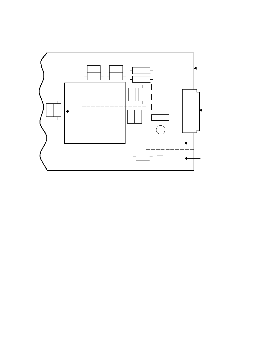
A�3
TVP3010
C3
C1
C4
C2
R1
D1
R2
C5
C12
C9
C6
R3
R4
R5
C11
+
L1
C7
C8
C10
Edge of Board
DB15 or DB9
Connector
Analog Power
Digital Power
P1
Figure A�2.
Typical Component Placement With Split-Power Plane
COMP and REF Terminals
A 0.1-
�
F ceramic capacitor should be connected between AV
DD
and COMP to avoid noise and
color-smearing problems. A 0.1-
�
F ceramic capacitor is also recommended between GND and REF to
further stabilize the output image. This 0.1-
�
F capacitor is needed for either internal or external voltage
references. These capacitor values may depend on the board layout; experimentation may be required in
order to determine optimum values.
Analog-Output Protection
The VIP analog output should be protected against high-energy discharges, such as those from monitor
arc-over or from hot-switching ac-coupled monitors.
The diode-protection circuit shown in Figure A�1 can prevent latch-up under severe discharge conditions
without adversely degrading analog transition times. The IN4148/9 parts are low-capacitance,
fast-switching diodes, which are also available in multiple-device packages (FSA250X or FSA270X) or
surface-mountable pairs (BAV99 or MMBD7001).

B�1
Appendix B
RCLK Frequency < VCLK Frequency
The VCLK, RCLK, and SCLK outputs generated by the TVP3010C or TVP3010M VIP are free-running
clocks. The video-control signals (i.e., HSYNC, VSYNC, and SYSBL) are normally generated from VCLK,
and a fixed relationship between video-control signals and VCLK can be expected. The VIP samples and
latches the Blank internal input on the falling edge of VCLK. It then looks at the internal RCLK signal to
determine when to enable or disable SCLK at the output terminal. The decision is determined when the
RCLK frequency is greater than or equal to the VCLK frequency. However, when the RCLK frequency is less
than the VCLK frequency, the appearance of the SCLK waveform at the output terminal (when SYSBL is
sampled low on the falling edge of VCLK) can vary (see Figures B�1 and B�2).
To avoid this variation in the SCLK output waveform, the RCLK and VCLK frequencies should be chosen
so that HTOTAL is evenly divisible by the ratio of the VCLK frequency to the RCLK frequency:
remainder of [ HTOTAL / (VCLK frequency / RCLK frequency)] = 0
For example, if HTOTAL is even, VCLK frequency = dot clock frequency/8 and RCLK frequency = dot clock
frequency/16. Then the above formula is satisfied.
NOTE:
When HTOTAL starts at zero, then the formula becomes:
remainder of [ (HTOTAL + 1) /( VCLK frequency / SCLK frequency) ] = 0.
VCLK
SYSBL
At Input
Terminal
RCLK
SCLK
Figure B�1. VCLK and SCLK Phase Relationship (Case 1)
VCLK
SYSBL
At Input
Terminal
RCLK
SCLK
Figure B�2. VCLK and SCLK Phase Relationship (Case 2)

C�1
Appendix C
Little-Endian and Big-Endian Data Formats
It is commonly known in the computer industry that there are two different formats for memory configuration:
little-endian (Intel microprocessor-based format) and big-endian (Motorola microprocessor-based format).
When the Texas Instruments programmable pixel bus was introduced on the TLC34075 video-interface
palette, it allowed little-endian-based graphics-board manufacturers to design a single graphics board that
could be programmed to support multiple resolutions and pixel depths. The connection of the pixel bus from
the video RAM to the palette device was not a problem until big-endian-based customers desired the same
capability to program their graphics designs from 1 bit/pixel (bpp), 2 bpp, 4 bpp, 8 bpp, 12 bpp, 16 bpp,
24 bpp, to 32 bpp.
For this reason, the TVP3010C and the TVP3010M video-interface palettes support both little- and
big-endian data formats on its pixel-bus/frame-buffer interface. The device defaults to little-endian mode at
reset (general-control register-bit 3 set to 0) to be compatible with most PC-based systems. Big-endian
mode operation can be achieved by configuring the device to the big-endian mode (general-control
register-bit 3 set to 1) and externally reverse wiring the pixel bus from video RAM to the VIP on the graphics
board.
The differences between the big-endian and little-endian data formats are illustrated in Figure C�1. The
figure shows that the data fields representing the individual pixels in the big-endian format are in the reverse
order of the little-endian format. Since the VIP always shifts data from low-numbered data fields to
high-numbered data fields, external swapping of the pixel bus (i.e., D31 connected to P0, D0 connected to
P31) ensures that the pixels are displayed on the monitor in the correct sequence. However, swapping the
big-endian pixel bus causes the bits within each data field to be reversed (i.e., MSB to LSB instead of LSB
to MSB). When general-control register-bit 3 is set to 1, unique circuitry within the TVP3010 corrects the bit
sequence in each data field as it is shifted into the part. This correction is bit-plane independent and occurs
regardless of whether 8, 4, 2, or 1 bit/pixel are being used.
Both the TVP3010C and TVP3010M also support 12-, 16-, and 24-bit true-/direct-color for both little- and
big-endian data formats on the pixel bus. By using the same wiring for big-endian operation as described
above, all true-/direct-color modes are made available without hardware modification. Tables 2�8 through
2�11 give the true-/direct-color bit definitions for all modes. For example, when in one of the 16-bit true-color
modes (big endian), the first RGB data word to be displayed is located in bits 16 � 31 of VRAM. Swapping
the external pixel bus when designing the graphics board ensures the correct display sequence by causing
the first RGB word to appear at pixel-bus inputs P(0 � 15). However, the bit order within the word is reversed.
When general-control register-bit 3 is set to 1, the bit sequence is automatically corrected by circuitry within
the VIP.
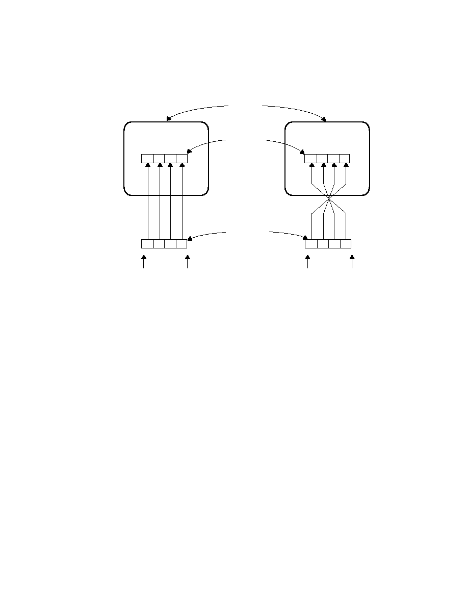
C�2
B0 B1 B2 B3
B0 B1 B2 B3
B0 B1 B2 B3
B3 B2 B1 B0
Monitor
Screen
4 Adjacent
Pixels
32-Bit Word
In Memory
0 - 7 8 -15 16 -23 24 -31
0 - 7 8 -15 16 -23 24 -31
LSB
MSB
LSB
MSB
Little Endian
Big Endian
Figure C�1. Little-Endian and Big-Endian Mapping of 4-Bit/Pixel
Pseudo-Color Data in Memory to Monitor Screen
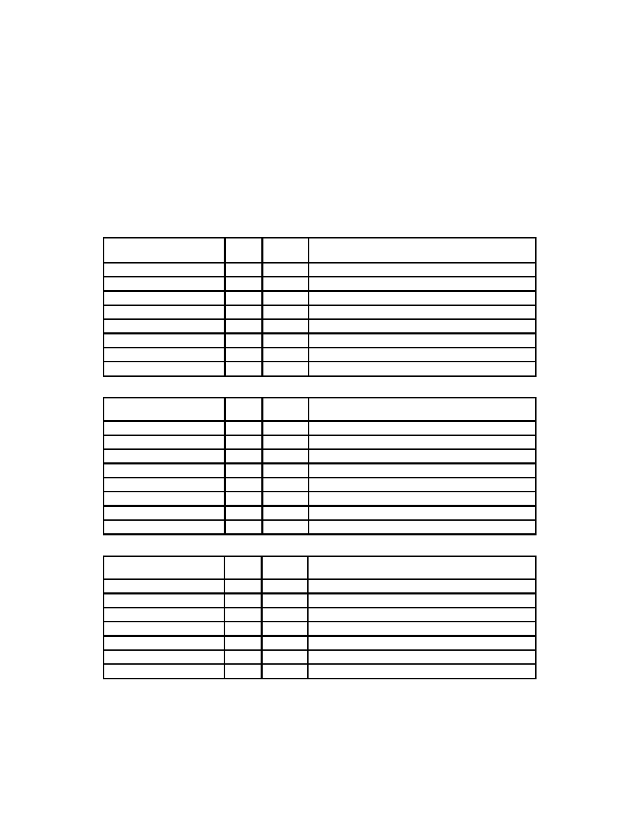
D�1
Appendix D
Examples: Register Settings
Table D �1. 8-Bit/Pixel Pseudo-Color (32-Bit Pixel Bus, 4:1)
Self-Clocked, LCLK and RCLK Enabled
REGISTER
INDEX
(HEX)
SETTING
(HEX)
DESCRIPTION
Input-Clock Selection
1A
xx
Any clock can be chosen
Output-Clock Selection
1B
52
RCLK = SCLK = /4, VCLK = /4 (VCLK could be different)
General Control
1D
20
Default settings
Auxiliary Control
29
09
Default settings, self-clocked, palette graphics, no zoom
Color-Key Control
38
10
Default settings, pointing to palette graphics
Multiplexer-Control Register 1
18
80
Pseudo-color
Multiplexer-Control Register 2
19
1B
8 bpp, 4:1, 32-bit pixel bus width
Configuration Register
1E
30
Enable LCLK and RCLK
Table D �2. 24-Bit True Color (32-Bit Pixel Bus, 1:1) Self-Clocked, RCLK = LCLK Internal
REGISTER
INDEX
(HEX)
SETTING
(HEX)
DESCRIPTION
Input-Clock Selection
1A
xx
Any clock can be chosen
Output-Clock Selection
1B
40
RCLK = SCLK = /1, VCLK = /1 (VCLK could be different)
General Control
1D
20
Default settings
Auxiliary Control
29
09
Default settings, self-clocked, palette graphics, no zoom
Color-Key Control
38
10
Default settings, pointing to palette graphics
Multiplexer-Control Register 1
18
46
24-bit true color
Multiplexer-Control Register 2
19
03
24-bit true color, 32-bit pixel-bus width
Configuration Register
1E
00
Default setting, RCLK internally connected to LCLK
Table D � 3. 24-Bit Direct Color (32-Bit Pixel Bus, 1:1) Self-Clocked, No Overlay
REGISTER
INDEX
(HEX)
SETTING
(HEX)
DESCRIPTION
Input-Clock Selection
1A
xx
Any clock can be chosen
Output-Clock Selection
1B
40
RCLK = SCLK = /1, VCLK = /1 (VCLK could be different)
General Control
1D
20
Default settings
Auxiliary Control
29
08
Self-clocked, no window, nonpalette graphics, no zoom
Color-Key Control
38
00
Disabled, pointing to nonpalette graphics
Multiplexer-Control Register 1
18
06
24-bit direct color
Multiplexer-Control Register 2
19
1B
24-bit direct color, 32-bit pixel bus width

D�2
Table D � 4. 24-Bit Direct Color (32-Bit Pixel Bus, 1:1) Self-Clocked, Overlay PSEL Switched
REGISTER
INDEX
(HEX)
SETTING
(HEX)
DESCRIPTION
Input-Clock Selection
1A
xx
Any clock can be chosen
Output-Clock Selection
1B
40
RCLK = SCLK = /1, VCLK = /1 (VCLK could be different)
General Control
1D
20
Default settings
Auxiliary Control
29
0C
Self-clocked, PSEL enabled, overlay when PSEL = 1
Color-Key Control
38
00
Disabled, pointing to nonpalette graphics
Multiplexer-Control Register 1
18
06
24-bit direct color
Multiplexer-Control Register 2
19
1B
24-bit direct color, 32-bit pixel bus width
Table D � 5. 24-Bit Direct Color (32-Bit Pixel Bus, 1:1) Externally-Clocked, VGA PSEL Switched
REGISTER
INDEX
(HEX)
SETTING
(HEX)
DESCRIPTION
Input-Clock Selection
1A
xx
Any clock can be chosen
Output-Clock Selection
1B
40
RCLK = SCLK = /1, VCLK = /1 (VCLK could be different)
General Control
1D
20
Default settings
Auxiliary Control
29
04
Externally clocked, PSEL enabled, VGA when PSEL = 1
Color-Key Control
38
00
Disabled, pointing to nonpalette graphics
Multiplexer-Control Register 1
18
06
24-bit direct color
Multiplexer-Control Register 2
19
9B
24-bit direct color, 32-bit pixel bus width
Configuration Register
1E
20
LCLK enabled for external timing mode
Table D � 6. 16-Bit Direct Color (32-Bit Pixel Bus, 2:1) Self-Clocked,
Overlay Auxiliary Window Switched
REGISTER
INDEX
(HEX)
SETTING
(HEX)
DESCRIPTION
Input-Clock Selection
1A
xx
Any clock can be chosen
Output-Clock Selection
1B
49
RCLK = SCLK = /2, VCLK = /2 (VCLK could be different)
General Control
1D
20
Default settings
Auxiliary Control
29
0A
Self-clocked, auxiliary window enabled, overlay in window
Color-Key Control
38
00
Disabled, pointing to nonpalette graphics
Multiplexer-Control Register 1
18
05
16-bit direct color � XGA format
Multiplexer-Control Register 2
19
03
16-bit direct color, 32-bit pixel-bus width
NOTE 1: For this mode, the auxiliary-window start and stop registers (Index 10 � 17) must be programmed with the
appropriate window coordinates (within active display) (see subsections 2.16.6 and 2.16.7).

E�1
Appendix E
Mechanical Data
FN (S-PQCC-J**)
PLASTIC QUAD CHIP CARRIER
4040005 / B 03/95
20 PIN SHOWN
0.026 (0,66)
0.032 (0,81)
D2 / E2
0.020 (0,51) MIN
0.180 (4,57) MAX
0.120 (3,05)
0.090 (2,29)
D2 / E2
0.013 (0,33)
0.021 (0,53)
Seating Plane
MAX
D2 / E2
0.219 (5,56)
0.169 (4,29)
0.319 (8,10)
0.469 (11,91)
0.569 (14,45)
0.369 (9,37)
MAX
0.356 (9,04)
0.456 (11,58)
0.656 (16,66)
0.008 (0,20) NOM
1.158 (29,41)
0.958 (24,33)
0.756 (19,20)
0.191 (4,85)
0.141 (3,58)
MIN
0.441 (11,20)
0.541 (13,74)
0.291 (7,39)
0.341 (8,66)
18
19
14
13
D
D1
1
3
9
E1
E
4
8
MIN
MAX
MIN
PINS
**
20
28
44
0.385 (9,78)
0.485 (12,32)
0.685 (17,40)
52
68
84
1.185 (30,10)
0.985 (25,02)
0.785 (19,94)
D / E
0.395 (10,03)
0.495 (12,57)
1.195 (30,35)
0.995 (25,27)
0.695 (17,65)
0.795 (20,19)
NO. OF
D1 / E1
0.350 (8,89)
0.450 (11,43)
1.150 (29,21)
0.950 (24,13)
0.650 (16,51)
0.750 (19,05)
0.004 (0,10)
M
0.007 (0,18)
0.050 (1,27)
NOTES: A. All linear dimensions are in inches (millimeters).
B. This drawing is subject to change without notice.
C. Falls within JEDEC MS-018

E�2
Mechanical Data (continued)
GA-GB (S-CPGA-P12 X 12)
CERAMIC PIN GRID ARRAY PACKAGE
4040114-5 / C 04/96
Down
Cavity
Up
Cavity
Down
Cavity
Cavity
Up
Outline
Small
Outline
Large
MAXIMUM PINS WITHIN MATRIX � 144
C1
0.025 (0,63)
0.060 (1,52)
0.060 (1,52)
0.040 (1,02)
C
B1
0.095 (2,41)
0.205 (5,21)
0.205 (5,21)
0.110 (2,79)
B
A1
1.180 (29,97)
1.235 (31,37)
1.280 (32,51)
DIM
MIN
MAX
Notes
1.240 (31,50)
A
A or A1 SQ
4 Places
DIA TYP
1.100 (27,94) TYP
0.050 (1,27) DIA
0.120 (3,05)
0.016 (0,41)
0.022 (0,55)
0.140 (3,56)
B or B1
C or C1
J
H
G
F
E
D
C
A
B
1
2
3
4
5
6
7
8
9
K
10
L
11 12
M
0.100 (2,54)
NOTES: A. All linear dimensions are in inches (millimeters).
B. This drawing is subject to change without notice.
C. Index mark may appear on top or bottom depending on package vendor.
D. Pins are located within 0.010 (0,25) diameter of true position relative to each other at maximum material
condition and within 0.030 (0,76) diameter relative to the edge of the ceramic.
E. This package can be hermetically sealed with metal lids or with ceramic lids using glass frit.
F. The pins can be gold plated or solder dipped.
G. Falls within MIL-STD-1835 CMGA4-PN and CMGA16-PN and JEDEC MO-067AD and MO-066AD,
respectively