Äîêóìåíòàöèÿ è îïèñàíèÿ www.docs.chipfind.ru
SN54ABTE16245, SN74ABTE16245
16-BIT INCIDENT-WAVE SWITCHING BUS TRANSCEIVERS
WITH 3-STATE OUTPUTS
SCBS226J JULY 1993 REVISED DECEMBER 2001
1
POST OFFICE BOX 655303
·
DALLAS, TEXAS 75265
D
Members of the Texas Instruments
Widebus
Family
D
Support the VME64 ETL Specification
D
Reduced, TTL-Compatible, Input Threshold
Range
D
High-Drive Outputs (I
OH
= 60 mA,
I
OL
= 90 mA) Support 25-
Incident-Wave
Switching
D
V
CC
BIAS Pin Minimizes Signal Distortion
During Live Insertion
D
Internal Pullup Resistor on OE Keeps
Outputs in High-Impedance State During
Power Up or Power Down
D
Distributed V
CC
and GND Pins Minimize
High-Speed Switching Noise
D
Equivalent 25-
Series Damping Resistor
on B Port
D
Bus Hold on Data Inputs Eliminates the
Need for External Pullup/Pulldown
Resistors
description
The 'ABTE16245 devices are 16-bit (dual-octal)
noninverting 3-state transceivers designed for
synchronous two-way communication between
data buses. The control-function implementation
minimizes external timing requirements. These
devices can be used as two 8-bit transceivers or
one 16-bit transceiver. They allow data transmission from the A bus to the B bus or from the B bus to the A bus,
depending on the logic level at the direction-control (DIR) input. The output-enable (OE) input can be used to
disable the device so that the buses are effectively isolated. When OE is low, the device is active.
The B port has an equivalent 25-
series output resistor to reduce ringing. Active bus-hold inputs also are on
the B port to hold unused or floating inputs at a valid logic level.
The A port provides for the precharging of the outputs via V
CC
BIAS, which establishes a voltage between 1.3 V
and 1.7 V when V
CC
is not connected.
Active bus-hold circuitry holds unused or undriven inputs at a valid logic state. Use of pullup or pulldown resistors
with the bus-hold circuitry is not recommended.
Copyright
2001, Texas Instruments Incorporated
PRODUCTION DATA information is current as of publication date.
Products conform to specifications per the terms of Texas Instruments
standard warranty. Production processing does not necessarily include
testing of all parameters.
Please be aware that an important notice concerning availability, standard warranty, and use in critical applications of
Texas Instruments semiconductor products and disclaimers thereto appears at the end of this data sheet.
Widebus is a trademark of Texas Instruments.
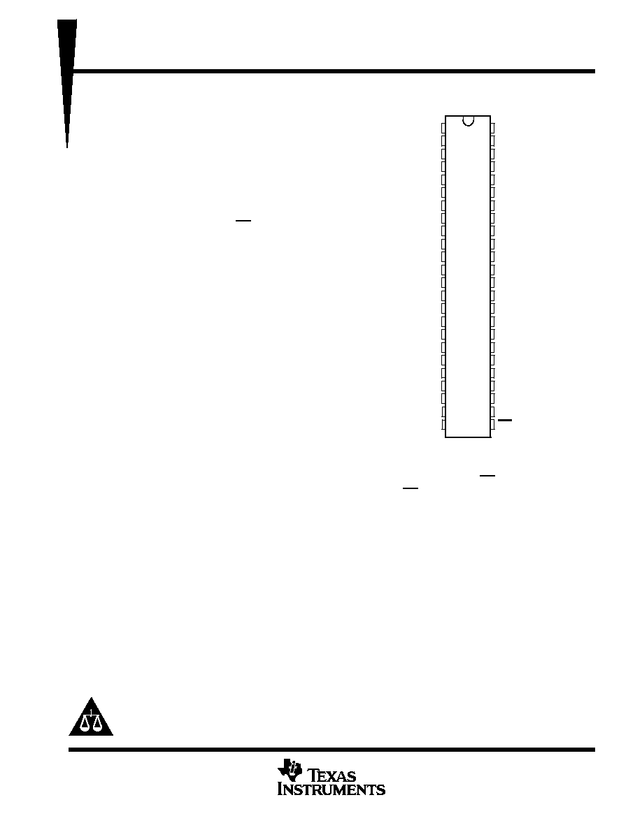
SN54ABTE16245 . . . WD PACKAGE
SN74ABTE16245 . . . DGG OR DL PACKAGE
(TOP VIEW)
1
2
3
4
5
6
7
8
9
10
11
12
13
14
15
16
17
18
19
20
21
22
23
24
48
47
46
45
44
43
42
41
40
39
38
37
36
35
34
33
32
31
30
29
28
27
26
25
1DIR
1B1
2B1
GND
1B2
2B2
V
CC
1B3
2B3
GND
1B4
2B4
1B5
2B5
GND
1B6
2B6
V
CC
1B7
2B7
GND
1B8
2B8
2DIR
V
CC
BIAS
1A1
2A1
GND
1A2
2A2
V
CC
1A3
2A3
GND
1A4
2A4
1A5
2A5
GND
1A6
2A6
V
CC
1A7
2A7
GND
1A8
2A8
OE
On products compliant to MIL-PRF-38535, all parameters are tested
unless otherwise noted. On all other products, production
processing does not necessarily include testing of all parameters.
SN54ABTE16245, SN74ABTE16245
16-BIT INCIDENT-WAVE SWITCHING BUS TRANSCEIVERS
WITH 3-STATE OUTPUTS
SCBS226J JULY 1993 REVISED DECEMBER 2001
2
POST OFFICE BOX 655303
·
DALLAS, TEXAS 75265
ORDERING INFORMATION
TA
PACKAGE
ORDERABLE
PART NUMBER
TOP-SIDE
MARKING
SSOP
DL
Tube
SN74ABTE16245DL
ABTE16245
40
°
C to 85
°
C
SSOP DL
Tape and reel
SN74ABTE16245DLR
ABTE16245
TSSOP DGG
Tape and reel
SN74ABTE16245DGGR
ABTE16245
55
°
C to 125
°
C
CFP WD
Tube
SNJ54ABTE16245WD
SNJ54ABTE16245WD
Package drawings, standard packing quantities, thermal data, symbolization, and PCB design guidelines are
available at www.ti.com/sc/package.
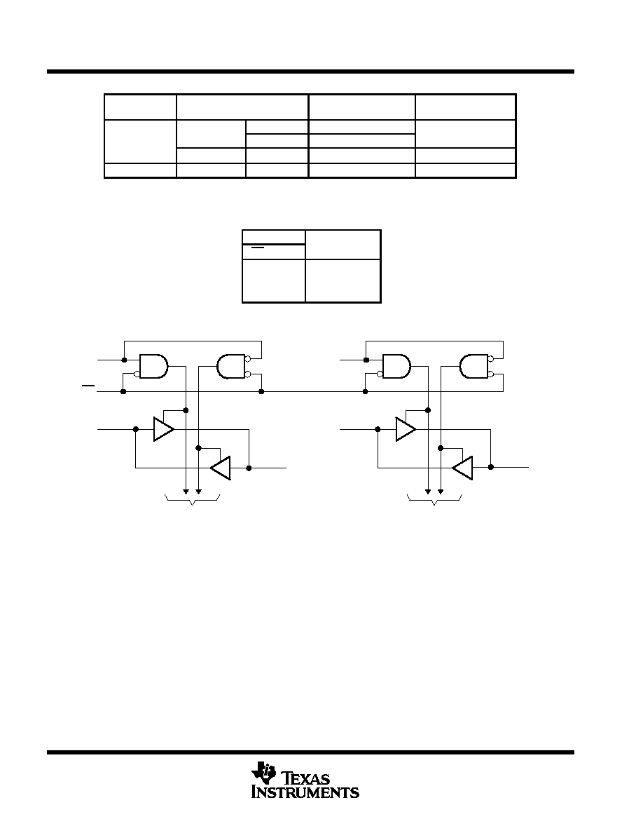
FUNCTION TABLE
(each 8-bit section)
INPUTS
OPERATION
OE
DIR
OPERATION
L
L
A data to B bus
L
H
B data to A bus
H
X
Isolation
logic diagram (positive logic)
To Seven Other Channels
1DIR
1B1
1A1
1
2
47
To Seven Other Channels
2DIR
2B1
2A1
24
3
46
OE
25
absolute maximum ratings over operating free-air temperature range (unless otherwise noted)
Supply voltage range, V
CC
and V
CC
BIAS
0.5 V to 7 V
. . . . . . . . . . . . . . . . . . . . . . . . . . . . . . . . . . . . . . . . . . . . .
Input voltage range, V
I
(except I/O ports) (see Note 1)
0.5 V to 7 V
. . . . . . . . . . . . . . . . . . . . . . . . . . . . . . . . . .
Voltage range applied to any output in the high state or power-off state, V
O
0.5 V to 5.5 V
. . . . . . . . . . . . . .
Current into any output in the low state, I
O
128 mA
. . . . . . . . . . . . . . . . . . . . . . . . . . . . . . . . . . . . . . . . . . . . . . . . . .
Input clamp current, I
IK
(V
I
< 0)
18 mA
. . . . . . . . . . . . . . . . . . . . . . . . . . . . . . . . . . . . . . . . . . . . . . . . . . . . . . . . . . .
Output clamp current, I
OK
(V
O
< 0)
50 mA
. . . . . . . . . . . . . . . . . . . . . . . . . . . . . . . . . . . . . . . . . . . . . . . . . . . . . . . .
Package thermal impedance,
JA
(see Note 2): DGG package
70
°
C/W
. . . . . . . . . . . . . . . . . . . . . . . . . . . . . . .
DL package
63
°
C/W
. . . . . . . . . . . . . . . . . . . . . . . . . . . . . . . . .
Storage temperature range, T
stg
65
°
C to 150
°
C
. . . . . . . . . . . . . . . . . . . . . . . . . . . . . . . . . . . . . . . . . . . . . . . . . . .
Stresses beyond those listed under "absolute maximum ratings" may cause permanent damage to the device. These are stress ratings only, and
functional operation of the device at these or any other conditions beyond those indicated under "recommended operating conditions" is not
implied. Exposure to absolute-maximum-rated conditions for extended periods may affect device reliability.
NOTES:
1. The input and output negative-voltage ratings may be exceeded if the input and output clamp-current ratings are observed.
2. The package thermal impedance is calculated in accordance with JESD 51-7.
SN54ABTE16245, SN74ABTE16245
16-BIT INCIDENT-WAVE SWITCHING BUS TRANSCEIVERS
WITH 3-STATE OUTPUTS
SCBS226J JULY 1993 REVISED DECEMBER 2001
3
POST OFFICE BOX 655303
·
DALLAS, TEXAS 75265
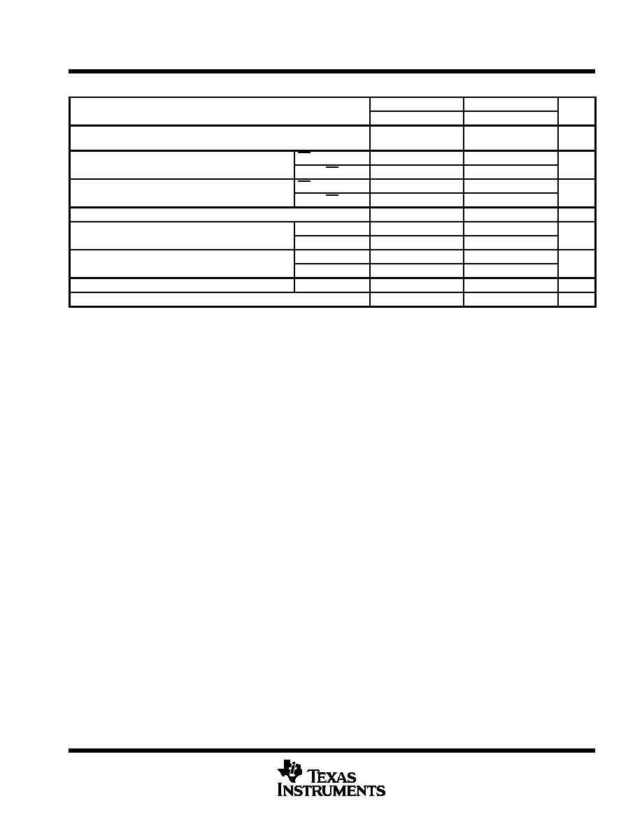
recommended operating conditions (see Note 3)
SN54ABTE16245
SN74ABTE16245
UNIT
MIN
NOM
MAX
MIN
NOM
MAX
UNIT
VCC,
VCCBIAS
Supply voltage
4.5
5
5.5
4.5
5
5.5
V
VIH
High level input voltage
OE
2
2
V
VIH
High-level input voltage
Except OE
1.6
1.6
V
VIL
Low level input voltage
OE
0.8
0.8
V
VIL
Low-level input voltage
Except OE
1.4
1.4
V
VI
Input voltage
0
VCC
0
VCC
V
IOH
High level output current
B bus
12
12
mA
IOH
High-level output current
A bus
24
60
mA
IOL
Low level output current
B bus
12
12
mA
IOL
Low-level output current
A bus
64
90
mA
t/
v
Input transition rise or fall rate
Outputs enabled
10
10
ns/V
TA
Operating free-air temperature
55
125
40
85
°
C
NOTE 3: All unused control inputs of the device must be held at VCC or GND to ensure proper device operation. Refer to the TI application report,
Implications of Slow or Floating CMOS Inputs, literature number SCBA004.
SN54ABTE16245, SN74ABTE16245
16-BIT INCIDENT-WAVE SWITCHING BUS TRANSCEIVERS
WITH 3-STATE OUTPUTS
SCBS226J JULY 1993 REVISED DECEMBER 2001
4
POST OFFICE BOX 655303
·
DALLAS, TEXAS 75265
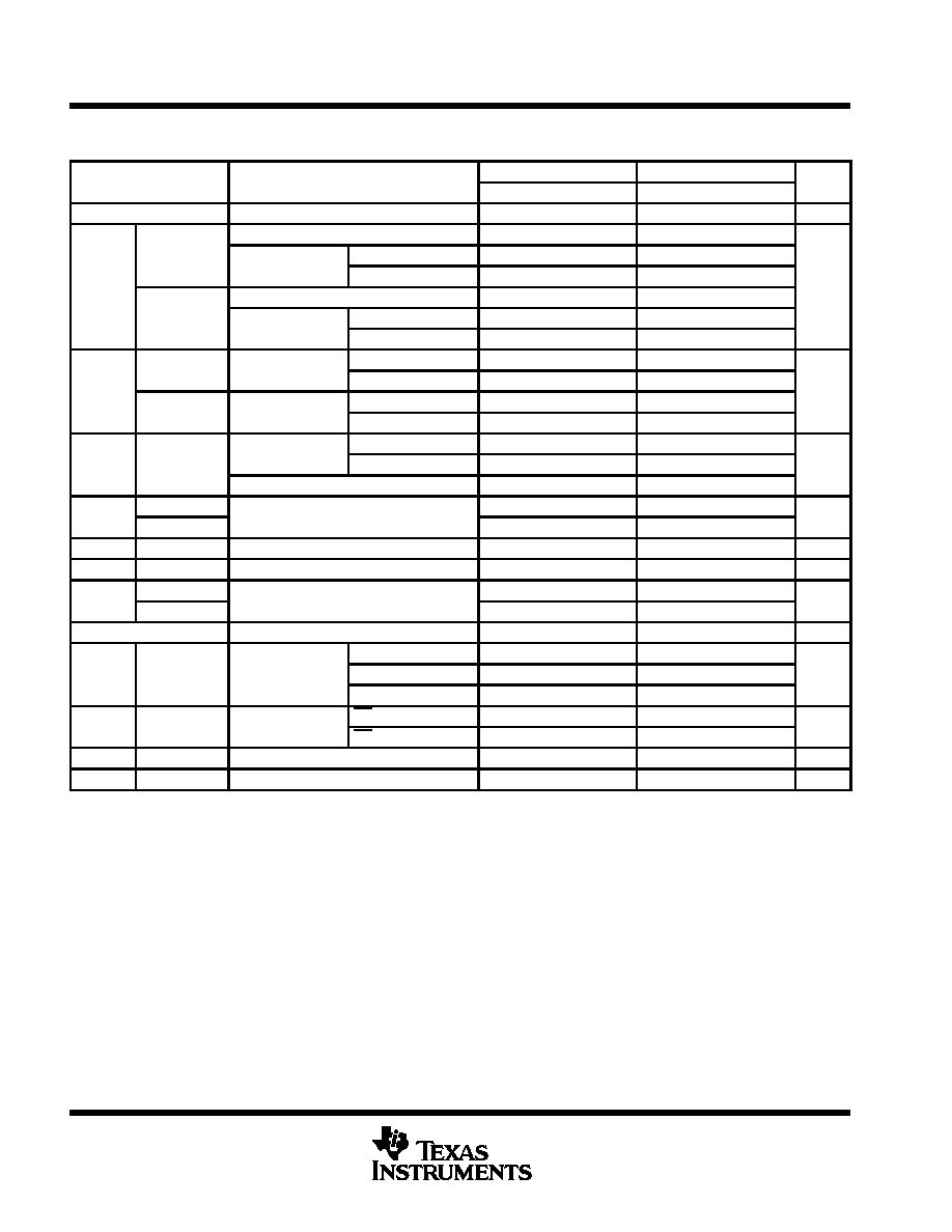
electrical characteristics over recommended operating free-air temperature range (unless
otherwise noted)
PARAMETER
TEST CONDITIONS
SN54ABTE16245
SN74ABTE16245
UNIT
PARAMETER
TEST CONDITIONS
MIN
TYP
MAX
MIN
TYP
MAX
UNIT
VIK
VCC = 4.5 V,
II = 18 mA
1.2
1.2
V
VCC = 5.5 V,
IOH = 100
µ
A
VCC0.2
VCC0.2
B port
VCC = 4 5 V
IOH = 1 mA
2.4
2.4
VOH
VCC = 4.5 V
IOH = 12 mA
2
2
V
VOH
VCC = 5.5 V,
IOH = 1 mA
4.5
4.5
V
A port
VCC = 4 5 V
IOH = 32 mA
2.4
2.4
VCC = 4.5 V
IOH = 64 mA
2
B port
VCC = 4 5 V
IOL = 1 mA
0.4
0.4
VOL
B port
VCC = 4.5 V
IOL = 12 mA
0.8
V
VOL
A port
VCC = 4 5 V
IOL = 64 mA
0.55
0.55
V
A port
VCC = 4.5 V
IOL = 90 mA
0.9
VCC = 4 5 V
VI = 0.8 V
100
100
II(hold)
B port
VCC = 4.5 V
VI = 2 V
100
100
µ
A
(
)
VCC = 5.5 V,
VI = 0 to 5.5 V
±
500
±
500
II
Control inputs
VCC = 5 5 V
VI = VCC or GND
±
1
±
1
µ
A
II
A or B ports
VCC = 5.5 V,
VI = VCC or GND
±
20
±
20
µ
A
IOZH
A port
VCC = 5.5 V,
VO = 2.7 V
10
10
µ
A
IOZL
A port
VCC = 5.5 V,
VO = 0.5 V
10
10
µ
A
IO
A port
VCC = 5 5 V
VO = 2 5 V
50
120
180
50
180
mA
IO
B port
VCC = 5.5 V,
VO = 2.5 V
25
52
90
25
90
mA
Ioff
VCC = 0, VI or VO
4.5 V, VCCBIAS = 0
±
100
±
100
µ
A
V
5 5 V I
0
Outputs high
28
36
28
36
ICC
A or B ports
VCC = 5.5 V, IO = 0,
VI = VCC or GND
Outputs low
38
48
38
48
mA
VI = VCC or GND
Outputs disabled
20
32
20
32
ICCD
A or B ports
VCC = 5 V,
OE high
0.02
0.02
mA/
ICCD
A or B ports
CC
,
CL = 50 pF
OE low
0.33
0.33
MHz
Ci
Control inputs
VI = 2.5 V or 0.5 V
10
2.5
4
pF
Cio
I/O ports
VO = 2.5 V or 0.5 V
13
4.5
8
pF
All typical values are at VCC = 5 V, TA = 25
°
C.
The parameters IOZH and IOZL include the input leakage current.
SN54ABTE16245, SN74ABTE16245
16-BIT INCIDENT-WAVE SWITCHING BUS TRANSCEIVERS
WITH 3-STATE OUTPUTS
SCBS226J JULY 1993 REVISED DECEMBER 2001
5
POST OFFICE BOX 655303
·
DALLAS, TEXAS 75265
live-insertion specifications over recommended operating free-air temperature range
PARAMETER
TEST CONDITIONS
SN54ABTE16245
SN74ABTE16245
UNIT
PARAMETER
TEST CONDITIONS
MIN
TYP
MAX
MIN
TYP
MAX
UNIT
ICC (VCCBIAS)
VCC = 0 to 4.5 V, VCCBIAS = 4.5 V to 5.5 V,
IO(DC) = 0
250
700
250
700
µ
A
ICC (VCCBIAS)
VCC = 4.5 V to 5.5 V, VCCBIAS = 4.5 V to 5.5 V,
IO(DC) = 0
20
20
µ
A
VO
A port
VCC = 0
VCCBIAS = 4.5 V to 5.5 V
1.1
1.5
1.9
1.1
1.5
1.9
V
VO
A port
VCC = 0
VCCBIAS = 4.75 V to 5.25 V
1.3
1.5
1.7
1.3
1.5
1.7
V
IO
A port
VCC = 0
VCCBIAS = 4 5 V
VO = 0
20
100
20
100
µ
A
IO
A port
VCC = 0,
VCCBIAS = 4.5 V
VO = 3 V
20
100
20
100
µ
A
All typical values are at VCC = 5 V, TA = 25
°
C.
VCC 0.5 V < VCCBIAS
switching characteristics over recommended ranges of supply voltage and operating free-air
temperature, C
L
= 50 pF (unless otherwise noted) (see Figure 2)
PARAMETER
FROM
(INPUT)
TO
(OUTPUT)
VCC = 5 V,
TA = 25
°
C
SN54ABTE16245
SN74ABTE16245
UNIT
(INPUT)
(OUTPUT)
MIN
TYP
MAX
MIN
MAX
MIN
MAX
tPLH
A
B
1.5
3.3
4.2
1.5
5.4
1.5
5.2
ns
tPHL
A
B
1.5
3.8
4.6
1.5
5.4
1.5
5.2
ns
tPLH
B
A
1.5
3
3.8
1.5
4.7
1.5
4.5
ns
tPHL
B
A
1.5
3.1
4
1.5
4.7
1.5
4.5
ns
tPZH
OE
A
2
3.9
5.3
2
6.4
2
6.2
ns
tPZL
OE
A
2
4.4
5.9
2
7
2
6.8
ns
tPZH
OE
B
2
4.5
6
2
7.3
2
7.1
ns
tPZL
OE
B
2
5
6.4
2
7.5
2
7.3
ns
tPHZ
OE
A
2
4.9
5.9
2
7
2
6.7
ns
tPLZ
OE
A
2
3.7
4.6
2
5.4
2
5.1
ns
tPHZ
OE
B
2
5.2
6.2
2
7.2
2
7
ns
tPLZ
OE
B
2
4
5
2
5.8
2
5.5
ns