"16-Bit Tri-Port Universal Bus Exchangers"
SN54ABTH32316, SN74ABTH32316
16-BIT TRI-PORT UNIVERSAL BUS EXCHANGERS
SCBS179E JUNE 1992 REVISED MAY 1997
1
POST OFFICE BOX 655303
·
DALLAS, TEXAS 75265
D
Members of the Texas Instruments
Widebus+
TM
Family
D
State-of-the-Art
EPIC-
B
TM
BiCMOS Design
Significantly Reduces Power Dissipation
D
UBE
TM
(Universal Bus Exchanger)
Combines D-Type Latches and D-Type
Flip-Flops for Operation in Transparent,
Latched, Clocked, or Clock-Enabled Mode
D
ESD Protection Exceeds 2000 V Per
MIL-STD-883, Method 3015
D
Latch-Up Performance Exceeds 500 mA
Per JEDEC Standard JESD-17
D
Typical V
OLP
(Output Ground Bounce)
< 0.8 V at V
CC
= 5 V, T
A
= 25
°
C
D
High-Impedance State During Power Up
and Power Down
D
Distributed V
CC
and GND Pin Configuration
Minimizes High-Speed Switching Noise
D
High-Drive Outputs (32-mA I
OH
, 64-mA I
OL
)
D
Bus Hold on Data Inputs Eliminates the
Need for External Pullup/Pulldown
Resistors
D
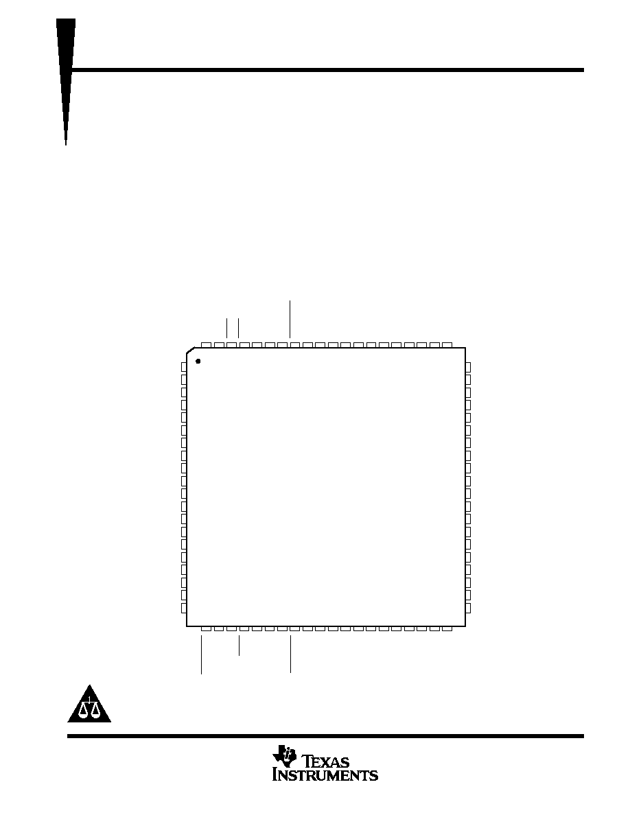
Package Options Include 80-Pin Plastic
Thin Quad Flat (PN) Package With
12
×
12-mm Body Using 0.5-mm Lead Pitch
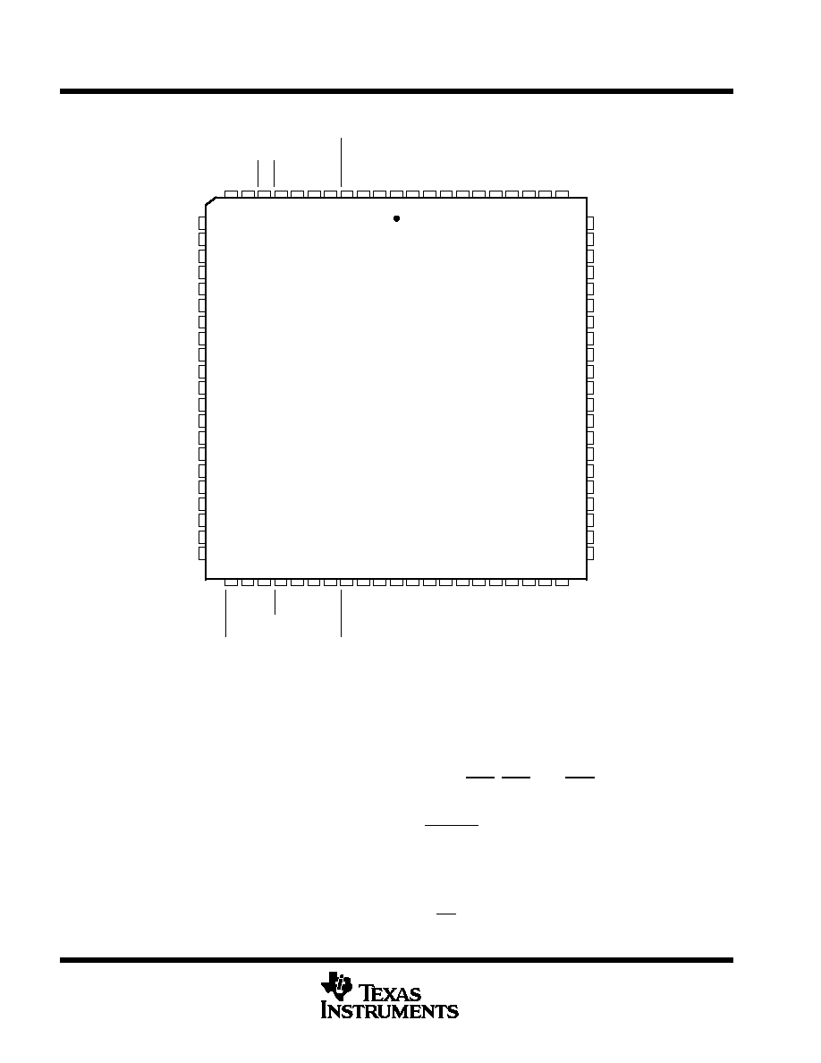
and 84-Pin Ceramic Quad Flat (HT) Package
22 23
C8
C7
C6
GND
C5
C4
C3
C2
C1
V
CC
GND
B16
B15
B14
B13
B12
GND
B11
B10
B9
60
59
58
57
56
55
54
53
52
51
50
49
48
47
46
45
44
43
42
41
24
1
2
3
4
5
6
7
8
9
10
11
12
13
14
15
16
17
18
19
20
A2
A3
A4
GND
A5
A6
A7
A8
A9
V
CC
GND
A10
A11
A12
A13
A14
GND
A15
A16
NC
25 26 27 28
'ABTH32316 . . . PN PACKAGE
(TOP VIEW)
GND
79 78 77 76 75
80
74
OEA
OEC
SELC
LEC
CLKC
CLKENC
NC
GND
B2
LEA
OEB
SELB
LEB
CLKB
CLKENB
NC
72 71 70
73
29 30 31 32 33
69 68
21
CLKENA
C15
67 66 65 64
34 35 36 37
B3
B4
B5
GND
C14
C13
C12
GND
A1
SELA
B6
B7
38 39 40
C1
1
C10
63 62 61
V
CC
C16
C9
CC
V
CLKA
B1
B8
NC No internal connection
Copyright
©
1997, Texas Instruments Incorporated
PRODUCTION DATA information is current as of publication date.
Products conform to specifications per the terms of Texas Instruments
standard warranty. Production processing does not necessarily include
testing of all parameters.
Widebus+, EPIC-
B, and UBE are trademarks of Texas Instruments Incorporated.
Please be aware that an important notice concerning availability, standard warranty, and use in critical applications of
Texas Instruments semiconductor products and disclaimers thereto appears at the end of this data sheet.
SN54ABTH32316, SN74ABTH32316
16-BIT TRI-PORT UNIVERSAL BUS EXCHANGERS
SCBS179E JUNE 1992 REVISED MAY 1997
2
POST OFFICE BOX 655303
·
DALLAS, TEXAS 75265
SN54ABTH32316 . . . HT PACKAGE
(TOP VIEW)
23 24
C8
C7
C6
GND
C5
C4
C3
C2
C1
V
CC
NC
GND
B16
B15
B14
B13
B12
GND
B11
B10
B9
63
62
61
60
59
58
57
56
55
54
53
52
51
50
49
48
47
46
45
44
43
25
1
2
3
4
5
6
7
8
9
10
11
12
13
14
15
16
17
18
19
20
21
A2
A3
A4
GND
A5
A6
A7
A8
A9
V
CC
NC
GND
A10
A11
A12
A13
A14
GND
A15
A16
NC
26 27 28 29
NC
83 82 81 80 79
84
78
OEA
OEC
SELC
LEC
CLKC
NC
B1
LEA
OEB
SELB
LEB
CLKB
CLKENB
NC
76 75 74
77
30 31 32 33 34
73 72
22
CLKENA
C16
71 70 69 68
35 36 37 38
B2
B3
B4
B5
C15
C14
C13
C12
A1
SELA
GND
B6
B8
39 40 41 42
GND
C1
1
C9
67 66 65 64
V
CC
GND
C10
CLKA
V
CC
GND
B7
NC
CLKENC
NC No internal connection
description
The 'ABTH32316 consist of three 16-bit registered input/output (I/O) ports. These registers combine D-type
latches and flip-flops to allow data flow in transparent, latch, and clock modes. Data from one input port can be
exchanged to one or more of the other ports. Because of the universal storage element, multiple combinations
of real-time and stored data can be exchanged among the three ports.
Data flow in each direction is controlled by the output-enable (OEA, OEB, and OEC), select-control (SELA,
SELB, and SELC), latch-enable (LEA, LEB, and LEC), and clock (CLKA, CLKB, and CLKC) inputs. The A data
register operates in the transparent mode when LEA is high. When LEA is low, data is latched if CLKA is held
at a high or low logic level. If LEA and clock-enable A (CLKENA) are low, data is stored on the low-to-high
transition of CLKA. Output data selection is accomplished by the select-control pins. All three ports have
active-low output enables, so when the output-enable input is low, the outputs are active; when the
output-enable input is high, the outputs are in the high-impedance state.
When V
CC
is between 0 and 2.1 V, the device is in the high-impedance state during power up or power down.
However, to ensure the high-impedance state above 2.1 V, OE should be tied to V
CC
through a pullup resistor;
the minimum value of the resistor is determined by the current-sinking capability of the driver.
SN54ABTH32316, SN74ABTH32316
16-BIT TRI-PORT UNIVERSAL BUS EXCHANGERS
SCBS179E JUNE 1992 REVISED MAY 1997
3
POST OFFICE BOX 655303
·
DALLAS, TEXAS 75265
description (continued)
Active bus-hold circuitry is provided to hold unused or floating data inputs at a valid logic level.
The SN54ABTH32316 is characterized for operation over the full military temperature range of 55
°
C to 125
°
C.
The SN74ABTH32316 is characterized for operation from 40
°
C to 85
°
C.
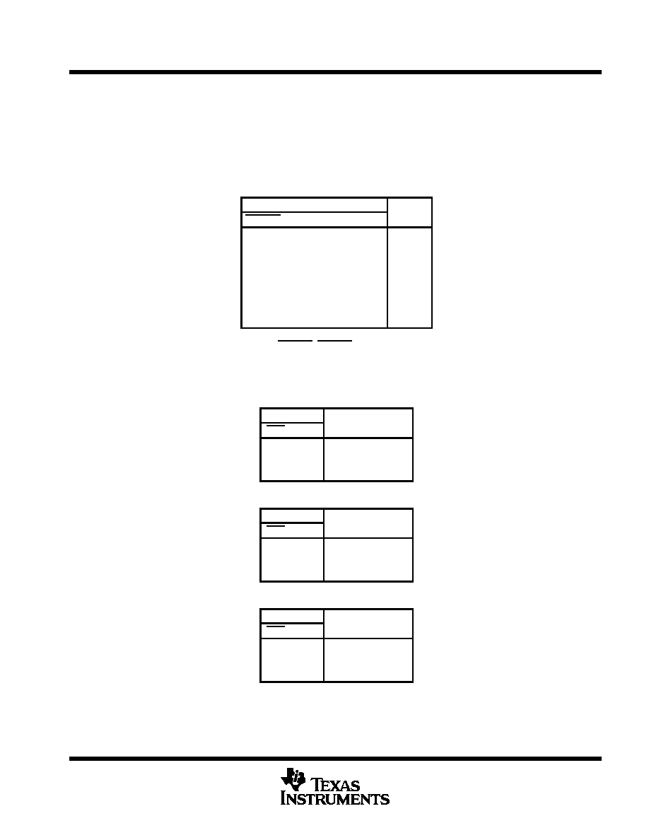
Function Tables
STORAGE
INPUTS
OUTPUT
CLKENA
CLKA
LEA
A
OUTPUT
H
X
L
X
Q0
L
L
L
L
L
L
H
H
X
H
L
X
Q0
X
L
L
X
Q0
X
X
H
L
L
X
X
H
H
H
A-port register shown. B and C ports are similar
but use CLKENB, CLKENC, CLKB, CLKC, LEB,
and LEC.
Output level before the indicated steady-state
input conditions were established
A-PORT OUTPUT
INPUTS
OUTPUT A
OEA
SELA
OUTPUT A
H
X
Z
L
H
Output of C register
L
L
Output of B register
B-PORT OUTPUT
INPUTS
OUTPUT B
OEB
SELB
OUTPUT B
H
X
Z
L
H
Output of A register
L
L
Output of C register
C-PORT OUTPUT
INPUTS
OUTPUT C
OEC
SELC
OUTPUT C
H
X
Z
L
H
Output of B register
L
L
Output of A register
SN54ABTH32316, SN74ABTH32316
16-BIT TRI-PORT UNIVERSAL BUS EXCHANGERS
SCBS179E JUNE 1992 REVISED MAY 1997
4
POST OFFICE BOX 655303
·
DALLAS, TEXAS 75265
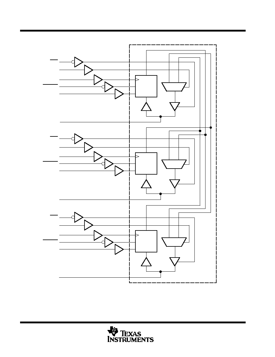
logic diagram (positive logic)
CLK
1 of 16 Channels
CE
C
OEA
SELA
CLKA
CLKENA
LEA
CLK
CE
C
OEB
SELB
CLKB
CLKENB
LEB
CLK
CE
C
OEC
SELC
CLKC
CLKENC
LEC
C1
B1
A1
77
76
74
73
75
52
24
25
27
28
26
32
78
79
22
21
23
80
Pin numbers shown are for the PN package.

SN54ABTH32316, SN74ABTH32316
16-BIT TRI-PORT UNIVERSAL BUS EXCHANGERS
SCBS179E JUNE 1992 REVISED MAY 1997
5
POST OFFICE BOX 655303
·
DALLAS, TEXAS 75265
absolute maximum ratings over operating free-air temperature range (unless otherwise noted)
Supply voltage range, V
CC
0.5 V to 7 V
. . . . . . . . . . . . . . . . . . . . . . . . . . . . . . . . . . . . . . . . . . . . . . . . . . . . . . . . . .
Input voltage range, V
I
(except I/O ports) (see Note 1)
0.5 V to 7 V
. . . . . . . . . . . . . . . . . . . . . . . . . . . . . . . . . .
Voltage range applied to any output in the high or power-off state, V
O
0.5 V to 5.5 V
. . . . . . . . . . . . . . . . . . .
Current into any output in the low state, I
O
: SN54ABTH32316 96
mA
. . . . . . . . . . . . . . . . . . . . . . . . . . . . . . . . .
SN74ABTH32316 128
mA
. . . . . . . . . . . . . . . . . . . . . . . . . . . . . . . .
Input clamp current, I
IK
(V
I
< 0)
18 mA
. . . . . . . . . . . . . . . . . . . . . . . . . . . . . . . . . . . . . . . . . . . . . . . . . . . . . . . . . . .
Output clamp current, I
OK
(V
O
< 0)
50 mA
. . . . . . . . . . . . . . . . . . . . . . . . . . . . . . . . . . . . . . . . . . . . . . . . . . . . . . . .
Package thermal impedance,
JA
(see Note 2): PN package
62
°
C/W
. . . . . . . . . . . . . . . . . . . . . . . . . . . . . . . . . .
Storage temperature range, T
stg
65
°
C to 150
°
C
. . . . . . . . . . . . . . . . . . . . . . . . . . . . . . . . . . . . . . . . . . . . . . . . . . .
Stresses beyond those listed under "absolute maximum ratings" may cause permanent damage to the device. These are stress ratings only, and
functional operation of the device at these or any other conditions beyond those indicated under "recommended operating conditions" is not
implied. Exposure to absolute-maximum-rated conditions for extended periods may affect device reliability.
NOTES:
1. The input and output negative-voltage ratings may be exceeded if the input and output clamp-current ratings are observed.
2. The package thermal impedance is calculated in accordance with EIA/JEDEC Std JESD51.
recommended operating conditions (see Note 3)
SN54ABTH32316
SN74ABTH32316
UNIT
MIN
MAX
MIN
MAX
UNIT
VCC
Supply voltage
4.5
5.5
4.5
5.5
V
VIH
High-level input voltage
2
2
V
VIL
Low-level input voltage
0.8
0.8
V
VI
Input voltage
0
VCC
0
VCC
V
IOH
High-level output current
24
32
mA
IOL
Low-level output current
48
64
mA
t/
v
Input transition rise or fall rate
Outputs enabled
10
10
ns/V
t/
VCC
Power-up ramp rate
200
200
µ
s/V
TA
Operating free-air temperature
55
125
40
85
°
C
NOTE 3: Unused control pins must be held high or low to prevent them from floating.