
SN54CBTD3384, SN74CBTD3384
10-BIT FET BUS SWITCHES
WITH LEVEL SHIFTING
SCDS025Q ≠ MAY 1995 ≠ REVISED JULY 2002
1
POST OFFICE BOX 655303
∑
DALLAS, TEXAS 75265
D
5-
Switch Connection Between Two Ports
D
TTL-Compatible Input Levels
D
Designed to Be Used in Level-Shifting
Applications
description/ordering information
The 'CBTD3384 devices provide ten bits of
high-speed TTL-compatible bus switching. The
low on-state resistance of the switches allows
connections to be made without adding
propagation delay. A diode to V
CC
is integrated on
the die to allow for level shifting from 5-V signals
at the device inputs to 3.3-V signals at the device
outputs.
These devices are organized as two 5-bit
switches with separate output-enable (OE)
inputs. When OE is low, the switch is on, and
port A is connected to port B. When OE is high, the
switch is open, and the high-impedance state
exists between the two ports.
ORDERING INFORMATION
TA
PACKAGE
ORDERABLE
PART NUMBER
TOP-SIDE
MARKING
SOIC
DW
Tube
SN74CBTD3384DW
CBTD3384
SOIC ≠ DW
Tape and reel
SN74CBTD3384DWR
CBTD3384
40
∞
C to 85
∞
C
SSOP ≠ DB
Tape and reel
SN74CBTD3384DBR
CC384
≠40
∞
C to 85
∞
C
SSOP (QSOP) ≠ DBQ
Tape and reel
SN74CBTD3384DBQR
CBTD3384
TSSOP ≠ PW
Tape and reel
SN74CBTD3384PWR
CC384
TVSOP ≠ DGV
Tape and reel
SN74CBTD3384DGVR
CC384
CDIP ≠ JT
Tube
SNJ54CBTD3384JT
SNJ54CBTD3384JT
≠55
∞
C to 125
∞
C
CFP ≠ W
Tube
SNJ54CBTD3384W
SNJ54CBTD3384W
LCCC ≠ FK
Tube
SNJ54CBTD3384FK
SNJ54CBTD3384FK
Package drawings, standard packing quantities, thermal data, symbolization, and PCB design guidelines are
available at www.ti.com/sc/package.
Copyright
2002, Texas Instruments Incorporated
PRODUCTION DATA information is current as of publication date.
Products conform to specifications per the terms of Texas Instruments
standard warranty. Production processing does not necessarily include
testing of all parameters.
Please be aware that an important notice concerning availability, standard warranty, and use in critical applications of
Texas Instruments semiconductor products and disclaimers thereto appears at the end of this data sheet.
SN54CBTD3384 . . . JT OR W PACKAGE
SN74CBTD3384 . . . DB, DBQ, DGV, DW, OR PW PACKAGE
(TOP VIEW)
1OE
1B1
1A1
1A2
1B2
1B3
1A3
1A4
1B4
1B5
1A5
GND
V
CC
2B5
2A5
2A4
2B4
2B3
2A3
2A2
2B2
2B1
2A1
2OE
1
2
3
4
5
6
7
8
9
10
11
12
24
23
22
21
20
19
18
17
16
15
14
13
SN54CBTD3384 . . . FK PACKAGE
(TOP VIEW)
3 2
1
13 14
5
6
7
8
9
10
11
2A4
2B4
2B3
NC
2A3
2A2
2B2
1A2
1B2
1B3
NC
1A3
1A4
1B4
4
15 16 17 18
1A5
GND
NC
2OE
2A1
2B1
1A1
1B1
1OE
NC
28 27 26
12
1B5
2B5
2A5
25
24
23
22
21
20
19
V
CC
NC ≠ No internal connection
On products compliant to MIL-PRF-38535, all parameters are tested
unless otherwise noted. On all other products, production
processing does not necessarily include testing of all parameters.
SN54CBTD3384, SN74CBTD3384
10-BIT FET BUS SWITCHES
WITH LEVEL SHIFTING
SCDS025Q ≠ MAY 1995 ≠ REVISED JULY 2002
2
POST OFFICE BOX 655303
∑
DALLAS, TEXAS 75265
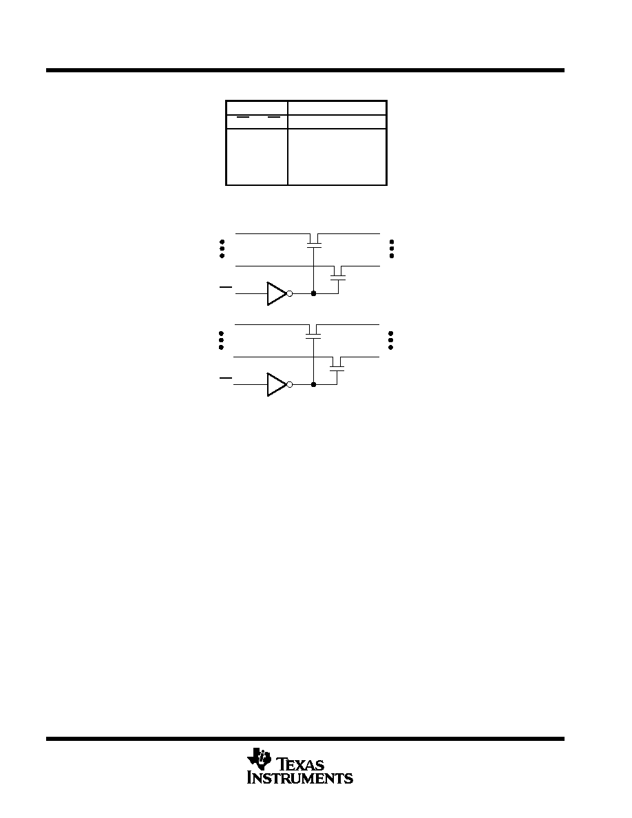
FUNCTION TABLE
(each 5-bit bus switch)
INPUTS
INPUTS/OUTPUTS
1OE
2OE
1B1≠1B5
2B1≠2B5
L
L
1A1≠1A5
2A1≠2A5
L
H
1A1≠1A5
Z
H
L
Z
2A1≠2A5
H
H
Z
Z
logic diagram (positive logic)
Pin numbers shown are for the DB, DBQ, DGV, DW, JT, PW, and W packages.
3
2
1A1
1B1
11
1A5
1
1OE
10
1B5
14
15
2A1
2B1
22
2A5
13
2OE
23
2B5
absolute maximum ratings over operating free-air temperature range (unless otherwise noted)
Supply voltage range, V
CC
≠0.5 V to 7 V
. . . . . . . . . . . . . . . . . . . . . . . . . . . . . . . . . . . . . . . . . . . . . . . . . . . . . . . . . .
Input voltage range, V
I
(see Note 1)
≠0.5 V to 7 V
. . . . . . . . . . . . . . . . . . . . . . . . . . . . . . . . . . . . . . . . . . . . . . . . . .
Continuous channel current
128 mA
. . . . . . . . . . . . . . . . . . . . . . . . . . . . . . . . . . . . . . . . . . . . . . . . . . . . . . . . . . . . . .
Input clamp current, I
IK
(V
I/O
< 0)
≠50 mA
. . . . . . . . . . . . . . . . . . . . . . . . . . . . . . . . . . . . . . . . . . . . . . . . . . . . . . . . .
Package thermal impedance,
JA
(see Note 2): DB package
63
∞
C/W
. . . . . . . . . . . . . . . . . . . . . . . . . . . . . . . . .
DBQ package
61
∞
C/W
. . . . . . . . . . . . . . . . . . . . . . . . . . . . . . . .
DGV package
86
∞
C/W
. . . . . . . . . . . . . . . . . . . . . . . . . . . . . . . .
DW package
46
∞
C/W
. . . . . . . . . . . . . . . . . . . . . . . . . . . . . . . . .
PW package
88
∞
C/W
. . . . . . . . . . . . . . . . . . . . . . . . . . . . . . . . .
Storage temperature range, T
stg
≠65
∞
C to 150
∞
C
. . . . . . . . . . . . . . . . . . . . . . . . . . . . . . . . . . . . . . . . . . . . . . . . . . .
Stresses beyond those listed under "absolute maximum ratings" may cause permanent damage to the device. These are stress ratings only, and
functional operation of the device at these or any other conditions beyond those indicated under "recommended operating conditions" is not
implied. Exposure to absolute-maximum-rated conditions for extended periods may affect device reliability.
NOTES:
1. The input and output negative-voltage ratings may be exceeded if the input and output clamp-current ratings are observed.
2. The package thermal impedance is calculated in accordance with JESD 51-7.

SN54CBTD3384, SN74CBTD3384
10-BIT FET BUS SWITCHES
WITH LEVEL SHIFTING
SCDS025Q ≠ MAY 1995 ≠ REVISED JULY 2002
3
POST OFFICE BOX 655303
∑
DALLAS, TEXAS 75265
recommended operating conditions (see Note 3)
SN54CBTD3384
SN74CBTD3384
UNIT
MIN
MAX
MIN
MAX
UNIT
VCC
Supply voltage
4.5
5.5
4.5
5.5
V
VIH
High-level control input voltage
2
2
V
VIL
Low-level control input voltage
0.8
0.8
V
TA
Operating free-air temperature
≠55
125
≠40
85
∞
C
In applications with fast edge rates, multiple outputs switching, and operating at high frequencies, the output may have little or no level-shifting
effect.
NOTE 3: All unused control inputs of the device must be held at VCC or GND to ensure proper device operation. Refer to the TI application report,
Implications of Slow or Floating CMOS Inputs, literature number SCBA004.
electrical characteristics over recommended operating free-air temperature range (unless
otherwise noted)
PARAMETER
TEST CONDITIONS
SN54CBTD3384
SN74CBTD3384
UNIT
PARAMETER
TEST CONDITIONS
MIN
TYP
MAX
MIN
TYP
MAX
UNIT
VIK
VCC = 4.5 V,
II = ≠18 mA
≠1.2
≠1.2
V
VOH
See Figure 2
II
VCC = 5.5 V,
VI = 5.5 V or GND
±
1
±
1
µ
A
ICC
VCC = 5.5 V,
IO = 0,
VI = VCC or GND
1.5
1.5
mA
ICC
Control inputs
VCC = 5.5 V, One input at 3.4 V,
Other inputs at VCC or GND
2.5
2.5
mA
Ci
Control inputs
VI = 3 V or 0
3
3
pF
Cio(OFF)
VO = 3 V or 0, OE = VCC
3.5
3.5
pF
ß
VI = 0
II = 64 mA
5
5
7
ronß
VCC = 4.5 V
VI = 0
II = 30 mA
5
5
7
VI = 2.4 V,
II = 15 mA
35
35
50
Typical values are at VCC = 5 V, TA = 25
∞
C.
This is the increase in supply current for each input that is at the specified TTL voltage level rather than VCC or GND.
ß Measured by the voltage drop between the A and B terminals at the indicated current through the switch. On-state resistance is determined by
the lowest voltage of the two (A or B) terminals.
switching characteristics over recommended ranges of supply voltage and operating free-air
temperature range, C
L
= 50 pF (unless otherwise noted) (see Figure 1)
PARAMETER
FROM
TO
SN54CBTD3384
SN74CBTD3384
UNIT
PARAMETER
(INPUT)
(OUTPUT)
MIN
MAX
MIN
MAX
UNIT
tpd∂
A or B
B or A
0.25
0.25
ns
ten
OE
A or B
2.2
9.7
2.3
7
ns
tdis
OE
A or B
1.5
8.6
1.7
5.3
ns
∂ The propagation delay is the calculated RC time constant of the typical on-state resistance of the switch and the specified load capacitance, when
driven by an ideal voltage source (zero output impedance).

SN54CBTD3384, SN74CBTD3384
10-BIT FET BUS SWITCHES
WITH LEVEL SHIFTING
SCDS025Q ≠ MAY 1995 ≠ REVISED JULY 2002
4
POST OFFICE BOX 655303
∑
DALLAS, TEXAS 75265
PARAMETER MEASUREMENT INFORMATION
VOH
VOL
From Output
Under Test
CL = 50 pF
(see Note A)
LOAD CIRCUIT
S1
7 V
Open
GND
500
500
tPLH
tPHL
Output
Control
Output
Waveform 1
S1 at 7 V
(see Note B)
Output
Waveform 2
S1 at Open
(see Note B)
tPZL
tPZH
tPLZ
tPHZ
3 V
0 V
VOH
VOL
0 V
VOL + 0.3 V
VOH ≠ 0.3 V
0 V
Input
3 V
3.5 V
VOLTAGE WAVEFORMS
PROPAGATION DELAY TIMES
VOLTAGE WAVEFORMS
ENABLE AND DISABLE TIMES
Output
tpd
tPLZ/tPZL
tPHZ/tPZH
Open
7 V
Open
TEST
S1
NOTES: A. CL includes probe and jig capacitance.
B. Waveform 1 is for an output with internal conditions such that the output is low except when disabled by the output control.
Waveform 2 is for an output with internal conditions such that the output is high except when disabled by the output control.
C. All input pulses are supplied by generators having the following characteristics: PRR
10 MHz, ZO = 50
, tr
2.5 ns, tf
2.5 ns.
D. The outputs are measured one at a time with one transition per measurement.
E. tPLZ and tPHZ are the same as tdis.
F. tPZL and tPZH are the same as ten.
G. tPLH and tPHL are the same as tpd.
1.5 V
1.5 V
1.5 V
1.5 V
1.5 V
1.5 V
1.5 V
1.5 V
Figure 1. Load Circuit and Voltage Waveforms

SN54CBTD3384, SN74CBTD3384
10-BIT FET BUS SWITCHES
WITH LEVEL SHIFTING
SCDS025Q ≠ MAY 1995 ≠ REVISED JULY 2002
5
POST OFFICE BOX 655303
∑
DALLAS, TEXAS 75265
TYPICAL CHARACTERISTICS
VCC ≠ Supply Voltage ≠ V
OUTPUT VOLTAGE HIGH
vs
SUPPLY VOLTAGE
V
OH
≠
Output V
oltage High
≠
V
TA = 85
∞
C
VCC ≠ Supply Voltage ≠ V
OUTPUT VOLTAGE HIGH
vs
SUPPLY VOLTAGE
TA = 25
∞
C
6 mA
12 mA
24 mA
VCC ≠ Supply Voltage ≠ V
OUTPUT VOLTAGE HIGH
vs
SUPPLY VOLTAGE
TA = 0
∞
C
100
µ
A
6 mA
12 mA
24 mA
100
µ
A
6 mA
12 mA
24 mA
4
3.75
3.5
3.25
3
2.75
2.5
2.25
2
1.75
1.5
4
3.75
3.5
3.25
3
2.75
2.5
2.25
2
1.75
1.5
4
3.75
3.5
3.25
3
2.75
2.5
2.25
2
1.75
1.5
4.5
4.75
5
5.25
5.5
5.75
4.5
4.75
5
5.25
5.5
5.75
4.5
4.75
5
5.25
5.5
5.75
V
OH
≠
Output V
oltage High
≠
V
V
OH
≠
Output V
oltage High
≠
V
100
µ
A
Figure 2. V
OH
Values