SN54LVCH244A, SN74LVCH244A (Rev. M)
SN54LVCH244A, SN74LVCH244A
OCTAL BUFFERS/DRIVERS
WITH 3 STATE OUTPUTS
SCES009M - JULY 1995 - REVISED OCTOBER 2003
1
POST OFFICE BOX 655303
·
DALLAS, TEXAS 75265
D
Operate From 1.65 V to 3.6 V
D
Inputs Accept Voltages to 5.5 V
D
Max t
pd
of 5.9 ns at 3.3 V
D
Typical V
OLP
(Output Ground Bounce)
<0.8 V at V
CC
= 3.3 V, T
A
= 25
°
C
D
Typical V
OHV
(Output V
OH
Undershoot)
>2 V at V
CC
= 3.3 V, T
A
= 25
°
C
D
Support Mixed-Mode Signal Operation on
All Ports (5-V Input/Output Voltage With
3.3-V V
CC
)
D
I
off
Supports Partial-Power-Down Mode
Operation
D
Bus Hold on Data Inputs Eliminates the
Need for External Pullup/Pulldown
Resistors
D
Latch-Up Performance Exceeds 250 mA Per
JESD 17
D
ESD Protection Exceeds JESD 22
- 2000-V Human-Body Model (A114-A)
- 200-V Machine Model (A115-A)
- 1000-V Charged-Device Model (C101)
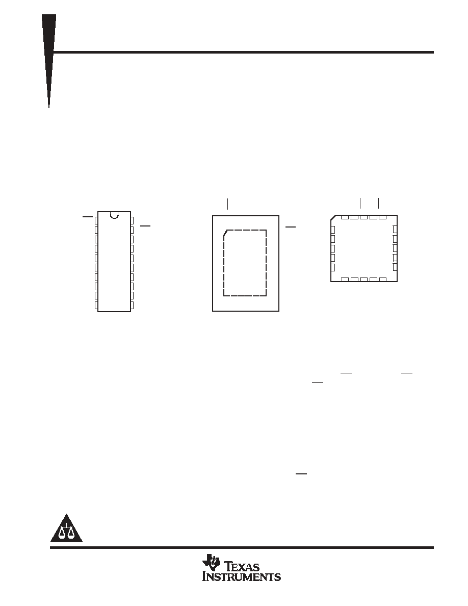
SN54LVCH244A . . . J OR W PACKAGE
SN74LVCH244A . . . DB, DBQ, DGV, DW,
NS, OR PW PACKAGE
(TOP VIEW)
SN54LVCH244A . . . FK PACKAGE
(TOP VIEW)
1
2
3
4
5
6
7
8
9
10
20
19
18
17
16
15
14
13
12
11
1OE
1A1
2Y4
1A2
2Y3
1A3
2Y2
1A4
2Y1
GND
V
CC
2OE
1Y1
2A4
1Y2
2A3
1Y3
2A2
1Y4
2A1
3
2
1 20 19
9 10 11 12 13
4
5
6
7
8
18
17
16
15
14
1Y1
2A4
1Y2
2A3
1Y3
1A2
2Y3
1A3
2Y2
1A4
2Y4
1A1
1OE
1Y4
2A2
2OE
2Y1
GND
2A1
V
CC
SN74LVCH244A . . . RGY PACKAGE
(TOP VIEW)
1
20
10
11
2
3
4
5
6
7
8
9
19
18
17
16
15
14
13
12
2OE
1Y1
2A4
1Y2
2A3
1Y3
2A2
1Y4
1A1
2Y4
1A2
2Y3
1A3
2Y2
1A4
2Y1
1OE
2A1
V
GND
CC
description/ordering information
The SN54LVCH244A octal buffer/line driver is designed for 2.7-V to 3.6-V V
CC
operation, and the
SN74LVCH244A octal buffer/line driver is designed for 1.65-V to 3.6-V V
CC
operation.
These devices are organized as two 4-bit line drivers with separate output-enable (OE) inputs. When OE is low,
these devices pass data from the A inputs to the Y outputs. When OE is high, the outputs are in the
high-impedance state.
Active bus-hold circuitry holds unused or undriven inputs at a valid logic state. Use of pullup or pulldown resistors
with the bus-hold circuitry is not recommended.
Inputs can be driven from either 3.3-V or 5-V devices. This feature allows the use of these devices as translators
in a mixed 3.3-V/5-V system environment.
These devices are fully specified for partial-power-down applications using I
off
. The I
off
circuitry disables the
outputs, preventing damaging current backflow through the devices when they are powered down.
To ensure the high-impedance state during power up or power down, OE should be tied to V
CC
through a pullup
resistor; the minimum value of the resistor is determined by the current-sinking capability of the driver.
Copyright
2003, Texas Instruments Incorporated
PRODUCTION DATA information is current as of publication date.
Products conform to specifications per the terms of Texas Instruments
standard warranty. Production processing does not necessarily include
testing of all parameters.
Please be aware that an important notice concerning availability, standard warranty, and use in critical applications of
Texas Instruments semiconductor products and disclaimers thereto appears at the end of this data sheet.
On products compliant to MIL PRF 38535, all parameters are tested
unless otherwise noted. On all other products, production
processing does not necessarily include testing of all parameters.
SN54LVCH244A, SN74LVCH244A
OCTAL BUFFERS/DRIVERS
WITH 3 STATE OUTPUTS
SCES009M - JULY 1995 - REVISED OCTOBER 2003
2
POST OFFICE BOX 655303
·
DALLAS, TEXAS 75265
description/ordering information (continued)
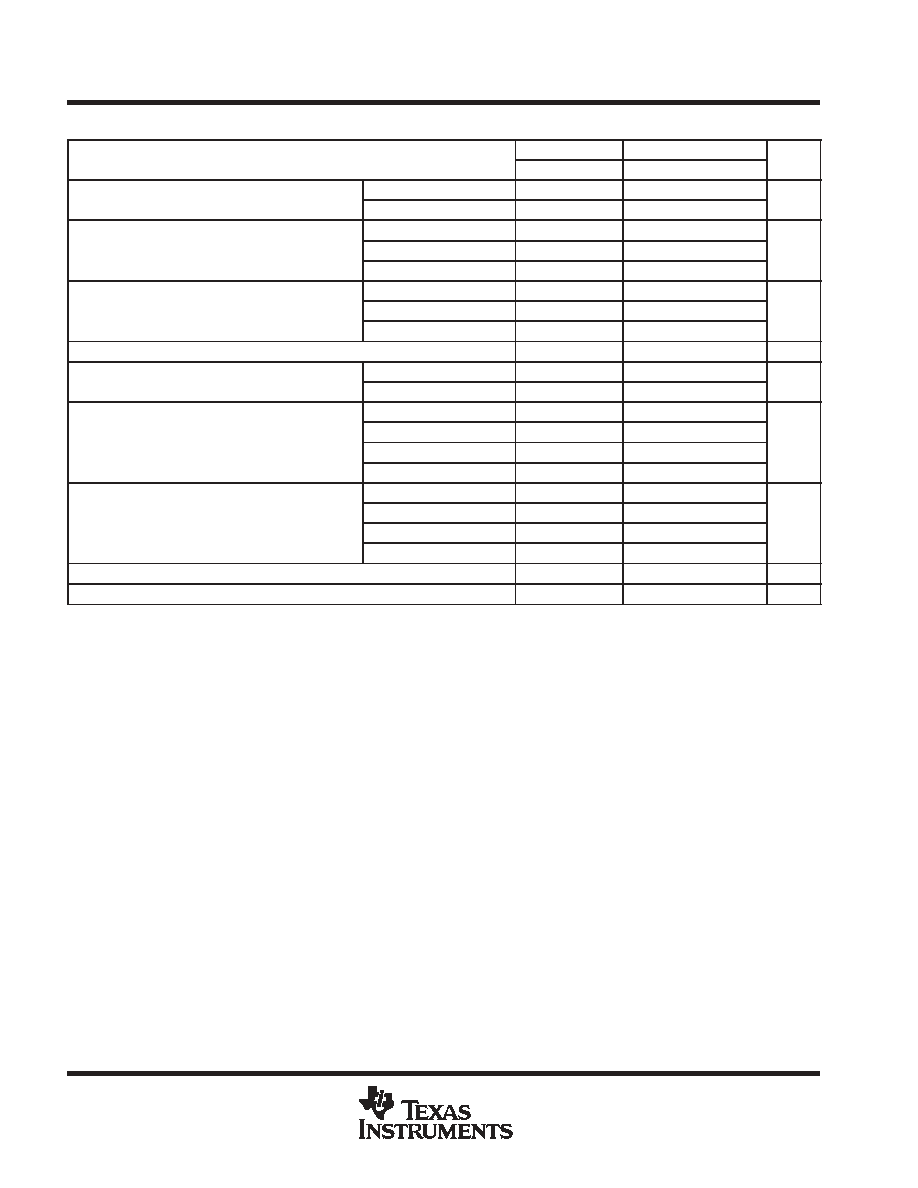
ORDERING INFORMATION
TA
PACKAGE
ORDERABLE
PART NUMBER
TOP-SIDE MARKING
QFN - RGY
Reel of 1000
SN74LVCH244ARGYR
LCH244A
SOIC - DW
Tube of 25
SN74LVCH244ADW
LVCH244A
SOIC - DW
Reel of 2000
SN74LVCH244ADWR
LVCH244A
SOP - NS
Reel of 2000
SN74LVCH244ANSR
LVCH244A
-40
°
C to 85
°
C
SSOP - DB
Reel of 2000
SN74LVCH244ADBR
LCH244A
-40
°
C to 85
°
C
SSOP (QSOP) - DBQ
Reel of 2500
SN74LVCH244ADBQR
LCH244A
Tube of 70
SN74LVCH244APW
TSSOP - PW
Reel of 2000
SN74LVCH244APWR
LCH244A
TSSOP - PW
Reel of 250
SN74LVCH244APWT
LCH244A
TVSOP - DGV
Reel of 2000
SN74LVCH244ADGVR
LCH244A
CDIP - J
Tube of 20
SNJ54LVCH244AJ
SNJ54LVCH244AJ
-55
°
C to 125
°
C
CFP - W
Tube of 85
SNJ54LVCH244AW
SNJ54LVCH244AW
-55 C to 125 C
LCCC - FK
Tube of 55
SNJ54LVCH244AFK
SNJ54LVCH244AFK
Package drawings, standard packing quantities, thermal data, symbolization, and PCB design guidelines are available
at www.ti.com/sc/package.
FUNCTION TABLE
(each buffer)
INPUTS
OUTPUT
OE
A
OUTPUT
Y
L
H
H
L
L
L
H
X
Z
logic diagram (positive logic)
1
2
18
1Y1
1OE
1A1
4
16
1Y2
1A2
6
14
1Y3
1A3
8
12
1Y4
1A4
19
11
9
2Y1
2OE
2A1
13
7
2Y2
2A2
15
5
2Y3
2A3
17
3
2Y4
2A4

SN54LVCH244A, SN74LVCH244A
OCTAL BUFFERS/DRIVERS
WITH 3 STATE OUTPUTS
SCES009M - JULY 1995 - REVISED OCTOBER 2003
3
POST OFFICE BOX 655303
·
DALLAS, TEXAS 75265
absolute maximum ratings over operating free-air temperature range (unless otherwise noted)
Supply voltage range, V
CC
-0.5 V to 6.5 V
. . . . . . . . . . . . . . . . . . . . . . . . . . . . . . . . . . . . . . . . . . . . . . . . . . . . . . . . .
Input voltage range, V
I
(see Note 1)
-0.5 V to 6.5 V
. . . . . . . . . . . . . . . . . . . . . . . . . . . . . . . . . . . . . . . . . . . . . . . . .
Voltage range applied to any output in the high-impedance or power-off state, V
O
(see Note 1)
-0.5 V to 6.5 V
. . . . . . . . . . . . . . . . . . . . . . . . . . . . . . . . . . . . . . . . . . . . . . . . . . . . . . . . . . . . . . . . . . .
Voltage range applied to any output in the high or low state, V
O
(see Notes 1 and 2)
-0.5 V to V
CC
+ 0.5 V
. . . . . . . . . . . . . . . . . . . . . . . . . . . . . . . . . . . . . . . . . . . . . . . . . . . . . . .
Input clamp current, I
IK
(V
I
< 0)
-50 mA
. . . . . . . . . . . . . . . . . . . . . . . . . . . . . . . . . . . . . . . . . . . . . . . . . . . . . . . . . . .
Output clamp current, I
OK
(V
O
< 0)
-50 mA
. . . . . . . . . . . . . . . . . . . . . . . . . . . . . . . . . . . . . . . . . . . . . . . . . . . . . . . .
Continuous output current, I
O
±
50 mA
. . . . . . . . . . . . . . . . . . . . . . . . . . . . . . . . . . . . . . . . . . . . . . . . . . . . . . . . . . . . .
Continuous current through V
CC
or GND
±
100 mA
. . . . . . . . . . . . . . . . . . . . . . . . . . . . . . . . . . . . . . . . . . . . . . . . . .
Package thermal impedance,
JA
(see Note 3): DB package
70
°
C/W
. . . . . . . . . . . . . . . . . . . . . . . . . . . . . . . . .
(see Note 3): DBQ package
68
°
C/W
. . . . . . . . . . . . . . . . . . . . . . . . . . . . . . . .
(see Note 3): DGV package
92
°
C/W
. . . . . . . . . . . . . . . . . . . . . . . . . . . . . . . .
(see Note 3): DW package
58
°
C/W
. . . . . . . . . . . . . . . . . . . . . . . . . . . . . . . . .
(see Note 3): NS package
60
°
C/W
. . . . . . . . . . . . . . . . . . . . . . . . . . . . . . . . .
(see Note 3): PW package
83
°
C/W
. . . . . . . . . . . . . . . . . . . . . . . . . . . . . . . . .
(see Note 4): RGY package
37
°
C/W
. . . . . . . . . . . . . . . . . . . . . . . . . . . . . . . .
Storage temperature range, T
stg
-65
°
C to 150
°
C
. . . . . . . . . . . . . . . . . . . . . . . . . . . . . . . . . . . . . . . . . . . . . . . . . . .
Stresses beyond those listed under "absolute maximum ratings" may cause permanent damage to the device. These are stress ratings only, and
functional operation of the device at these or any other conditions beyond those indicated under "recommended operating conditions" is not
implied. Exposure to absolute-maximum-rated conditions for extended periods may affect device reliability.
NOTES:
1. The input negative-voltage and output voltage ratings may be exceeded if the input and output current ratings are observed.
2. The value of VCC is provided in the recommended operating conditions table.
3. The package thermal impedance is calculated in accordance with JESD 51-7.
4. The package thermal impedance is calculated in accordance with JESD 51-5.
SN54LVCH244A, SN74LVCH244A
OCTAL BUFFERS/DRIVERS
WITH 3 STATE OUTPUTS
SCES009M - JULY 1995 - REVISED OCTOBER 2003
4
POST OFFICE BOX 655303
·
DALLAS, TEXAS 75265
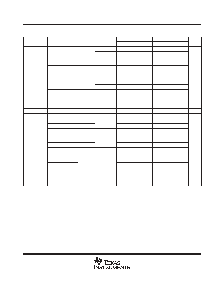
recommended operating conditions (see Note 5)
SN54LVCH244A
SN74LVCH244A
UNIT
MIN
MAX
MIN
MAX
UNIT
VCC
Supply voltage
Operating
2
3.6
1.65
3.6
V
VCC
Supply voltage
Data retention only
1.5
1.5
V
VCC = 1.65 V to 1.95 V
0.65
×
VCC
VIH
High-level input voltage
VCC = 2.3 V to 2.7 V
1.7
V
VIH
High-level input voltage
VCC = 2.7 V to 3.6 V
2
2
V
VCC = 1.65 V to 1.95 V
0.35
×
VCC
VIL
Low-level input voltage
VCC = 2.3 V to 2.7 V
0.7
V
VIL
Low-level input voltage
VCC = 2.7 V to 3.6 V
0.8
0.8
V
VI
Input voltage
0
5.5
0
5.5
V
VO
Output voltage
High or low state
0
VCC
0
VCC
V
VO
Output voltage
3-state
0
5.5
0
5.5
V
VCC = 1.65 V
-4
IOH
High-level output current
VCC = 2.3 V
-8
mA
IOH
High-level output current
VCC = 2.7 V
-12
-12
mA
VCC = 3 V
-24
-24
VCC = 1.65 V
4
IOL
Low-level output current
VCC = 2.3 V
8
mA
IOL
Low-level output current
VCC = 2.7 V
12
12
mA
VCC = 3 V
24
24
t/
v
Input transition rise or fall rate
10
10
ns/V
TA
Operating free-air temperature
-55
125
-40
85
°
C
NOTE 5: All unused control inputs of the device must be held at VCC or GND to ensure proper device operation. Refer to the TI application report,
Implications of Slow or Floating CMOS Inputs, literature number SCBA004.
SN54LVCH244A, SN74LVCH244A
OCTAL BUFFERS/DRIVERS
WITH 3 STATE OUTPUTS
SCES009M - JULY 1995 - REVISED OCTOBER 2003
5
POST OFFICE BOX 655303
·
DALLAS, TEXAS 75265
electrical characteristics over recommended operating free-air temperature range (unless
otherwise noted)
PARAMETER
TEST CONDITIONS
VCC
SN54LVCH244A
SN74LVCH244A
UNIT
PARAMETER
TEST CONDITIONS
VCC
MIN
TYP
MAX
MIN
TYP
MAX
UNIT
IOH = -100 A
1.65 V to 3.6 V
VCC-0.2
IOH = -100
µ
A
2.7 V to 3.6 V
VCC-0.2
IOH = -4 mA
1.65 V
1.2
VOH
IOH = -8 mA
2.3 V
1.7
V
VOH
IOH = -12 mA
2.7 V
2.2
2.2
V
IOH = -12 mA
3 V
2.4
2.4
IOH = -24 mA
3 V
2.2
2.2
IOL = 100 A
1.65 V to 3.6 V
0.2
IOL = 100
µ
A
2.7 V to 3.6 V
0.2
VOL
IOL = 4 mA
1.65 V
0.45
V
VOL
IOL = 8 mA
2.3 V
0.7
V
IOL = 12 mA
2.7 V
0.4
0.4
IOL = 24 mA
3 V
0.55
0.55
II
VI = 0 to 5.5 V
3.6 V
±
5
±
5
µ
A
Ioff
VI or VO = 5.5 V
0
±
10
µ
A
VI = 0.58 V
1.65 V
VI = 1.07 V
1.65 V
VI = 0.7 V
2.3 V
45
II(hold)
VI = 1.7 V
2.3 V
-45
µ
A
II(hold)
VI = 0.8 V
3 V
75
75
µ
A
VI = 2 V
3 V
-75
-75
VI = 0 to 3.6 V§
3..6 V
±
500
±
500
IOZ
VO = 0 to 5.5 V
3.6 V
±
15
±
10
µ
A
ICC
VI = VCC or GND
IO = 0
3.6 V
10
10
A
ICC
3.6 V
VI
5.5 V¶
IO = 0
3.6 V
10
10
µ
A
ICC
One input at VCC - 0.6 V,
Other inputs at VCC or GND
2.7 V to 3.6 V
500
500
µ
A
Ci
VI = VCC or GND
3.3 V
4
12
4
pF
Co
VO = VCC or GND
3.3 V
5.5
12
5.5
pF
All typical values are at VCC = 3.3 V, TA = 25
°
C.
This information was not available at the time of publication.
§ This is the bus-hold maximum dynamic current required to switch the input from one state to another.
¶ This applies in the disabled state only.