www.ti.com
FEATURES
1
2
3
4
5
6
7
8
9
10
20
19
18
17
16
15
14
13
12
11
OE
1Q
1D
2D
2Q
3Q
3D
4D
4Q
GND
V
CC
8Q
8D
7D
7Q
6Q
6D
5D
5Q
CLK
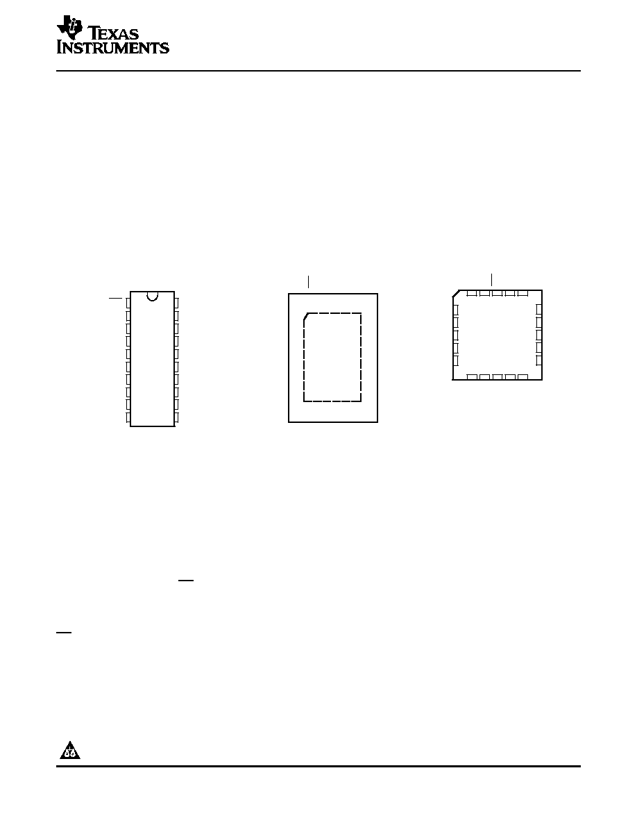
SN54LVC374A . . . J OR W PACKAGE
SN74LVC374A . . . DB, DGV, DW, N, NS,
OR PW PACKAGE
(TOP VIEW)
SN54LVC374A . . . FK PACKAGE
(TOP VIEW)
3
2
1 20 19
9 10 11 12 13
4
5
6
7
8
18
17
16
15
14
1D
1Q
OE
5Q
5D
8Q
4Q
GND
CLK
V
CC
8D
7D
7Q
6Q
6D
SN74LVC374A . . . RGY PACKAGE
(TOP VIEW)
1
20
10
11
2
3
4
5
6
7
8
9
19
18
17
16
15
14
13
12
8Q
8D
7D
7Q
6Q
6D
5D
5Q
1Q
1D
2D
2Q
3Q
3D
4D
4Q
CLK
V
GND
CC
OE
2D
2Q
3Q
3D
4D
DESCRIPTION/ORDERING INFORMATION
SN54LVC374A, SN74LVC374A
OCTAL EDGE-TRIGGERED D-TYPE FLIP-FLOPS
WITH 3-STATE OUTPUTS
SCAS296N ≠ JANUARY 1993 ≠ REVISED MAY 2005
∑
I
off
Supports Partial-Power-Down Mode
Operation
∑
Operate From 1.65 V to 3.6 V
∑
Latch-Up Performance Exceeds 250 mA Per
∑
Inputs Accept Voltages to 5.5 V
JESD 17
∑
Max t
pd
of 6.5 ns at 3.3 V
∑
ESD Protection Exceeds JESD 22
∑
Typical V
OLP
(Output Ground Bounce)
≠ 2000-V Human-Body Model (A114-A)
<0.8 V at V
CC
= 3.3 V, T
A
= 25∞C
≠ 200-V Machine Model (A115-A)
∑
Typical V
OHV
(Output V
OH
Undershoot)
>2 V at V
CC
= 3.3 V, T
A
= 25∞C
≠ 1000-V Charged-Device Model (C101)
∑
Support Mixed-Mode Signal Operation on
All Ports (5-V Input/Output Voltage
With 3.3-V V
CC
)
The SN54LVC374A octal edge-triggered D-type flip-flop is designed for 2.7-V to 3.6-V V
CC
operation, and the
SN74LVC374A octal edge-triggered D-type flip-flop is designed for 1.65-V to 3.6-V V
CC
operation.
These devices feature 3-state outputs designed specifically for driving highly capacitive or relatively
low-impedance loads. These devices are particularly suitable for implementing buffer registers, input/output (I/O)
ports, bidirectional bus drivers, and working registers.
On the positive transition of the clock (CLK) input, the Q outputs are set to the logic levels set up at the data (D)
inputs.
A buffered output-enable (OE) input can be used to place the eight outputs in either a normal logic state (high or
low logic levels) or the high-impedance state. In the high-impedance state, the outputs neither load nor drive the
bus lines significantly. The high-impedance state and increased drive provide the capability to drive bus lines
without interface or pullup components.
OE does not affect internal operations of the latch. Old data can be retained or new data can be entered while
the outputs are in the high-impedance state.
Inputs can be driven from either 3.3-V or 5-V devices. This feature allows the use of these devices as translators
in a mixed 3.3-V/5-V system environment.
Please be aware that an important notice concerning availability, standard warranty, and use in critical applications of Texas
Instruments semiconductor products and disclaimers thereto appears at the end of this data sheet.
PRODUCTION DATA information is current as of publication date.
Copyright © 1993≠2005, Texas Instruments Incorporated
Products conform to specifications per the terms of the Texas
On products compliant to MIL-PRF-38535, all parameters are
Instruments standard warranty. Production processing does not
tested unless otherwise noted. On all other products, production
necessarily include testing of all parameters.
processing does not necessarily include testing of all parameters.

www.ti.com
DESCRIPTION/ORDERING INFORMATION (CONTINUED)
OE
To Seven Other Channels
1
11
3
2
CLK
1D
C1
1D
1Q
SN54LVC374A, SN74LVC374A
OCTAL EDGE-TRIGGERED D-TYPE FLIP-FLOPS
WITH 3-STATE OUTPUTS
SCAS296N ≠ JANUARY 1993 ≠ REVISED MAY 2005
These devices are fully specified for partial-power-down applications using I
off
. The I
off
circuitry disables the
outputs, preventing damaging current backflow through the devices when they are powered down.
To ensure the high-impedance state during power up or power down, OE should be tied to V
CC
through a pullup
resistor; the minimum value of the resistor is determined by the current-sinking capability of the driver.
ORDERING INFORMATION
T
A
PACKAGE
(1)
ORDERABLE PART NUMBER
TOP-SIDE MARKING
PDIP ≠ N
Tube of 20
SN74LVC374AN
SN74LVC374AN
QFN ≠ RGY
Reel of 1000
SN74LVC374ARGYR
LC374A
Tube of 25
SN74LVC374ADW
SOIC ≠ DW
LVC374A
Reel of 2000
SN74LVC374ADWR
SOP ≠ NS
Reel of 2000
SN74LVC374ANSR
LVC374A
≠40∞C to 85∞C
SSOP ≠ DB
Reel of 2000
SN74LVC374ADBR
LC374A
Tube of 70
SN74LVC374APW
TSSOP ≠ PW
Reel of 2000
SN74LVC374APWR
LC374A
Reel of 250
SN74LVC374APWT
TVSOP ≠ DGV
Reel of 2000
SN74LVC374ADGVR
LC374A
CDIP ≠ J
Tube of 20
SNJ54LVC374AJ
SNJ54LVC374AJ
≠55∞C to 125∞C
CFP ≠ W
Tube of 85
SNJ54LVC374AW
SNJ54LVC374AW
LCCC ≠ FK
Tube of 55
SNJ54LVC374AFK
SNJ54LVC374AFK
(1)
Package drawings, standard packing quantities, thermal data, symbolization, and PCB design guidelines are available at
www.ti.com/sc/package.
FUNCTION TABLE (EACH FLIP-FLOP)
INPUTS
OUTPUT
Q
OE
CLK
D
L
H
H
L
L
L
L
H or L
X
Q
0
H
X
X
Z
LOGIC DIAGRAM (POSITIVE LOGIC)
2
www.ti.com
Absolute Maximum Ratings
(1)
SN54LVC374A, SN74LVC374A
OCTAL EDGE-TRIGGERED D-TYPE FLIP-FLOPS
WITH 3-STATE OUTPUTS
SCAS296N ≠ JANUARY 1993 ≠ REVISED MAY 2005
over operating free-air temperature range (unless otherwise noted)
MIN
MAX
UNIT
V
CC
Supply voltage range
≠0.5
6.5
V
V
I
Input voltage range
(2)
≠0.5
6.5
V
V
O
Voltage range applied to any output in the high-impedance or power-off state
(2) (3)
≠0.5
6.5
V
V
O
Voltage range applied to any output in the high or low state
≠0.5
V
CC
+ 0.5
V
I
IK
Input clamp current
V
I
< 0
≠50
mA
I
OK
Output clamp current
V
O
< 0
≠50
mA
I
O
Continuous output current
±50
mA
Continuous current through V
CC
or GND
±100
mA
DB package
(4)
70
DGV package
(4)
92
DW package
(4)
58
JA
Package thermal impedance
N package
(4)
69
∞C/W
NS package
(4)
60
PW package
(4)
83
RGY package
(5)
37
T
stg
Storage temperature range
≠65
150
∞C
(1)
Stresses beyond those listed under "absolute maximum ratings" may cause permanent damage to the device. These are stress ratings
only, and functional operation of the device at these or any other conditions beyond those indicated under "recommended operating
conditions" is not implied. Exposure to absolute-maximum-rated conditions for extended periods may affect device reliability.
(2)
The input negative-voltage and output voltage ratings may be exceeded if the input and output current ratings are observed.
(3)
The value of V
CC
is provided in the recommended operating conditions table.
(4)
The package thermal impedance is calculated in accordance with JESD 51-7.
(5)
The package thermal impedance is calculated in accordance with JESD 51-5.
3

www.ti.com
Recommended Operating Conditions
(1)
SN54LVC374A, SN74LVC374A
OCTAL EDGE-TRIGGERED D-TYPE FLIP-FLOPS
WITH 3-STATE OUTPUTS
SCAS296N ≠ JANUARY 1993 ≠ REVISED MAY 2005
SN54LVC374A
SN74LVC374A
UNIT
MIN
MAX
MIN
MAX
Operating
2
3.6
1.65
3.6
V
CC
Supply voltage
V
Data retention only
1.5
1.5
V
CC
= 1.65 V to 1.95 V
0.65 ◊ V
CC
V
IH
High-level input voltage
V
CC
= 2.3 V to 2.7 V
1.7
V
V
CC
= 2.7 V to 3.6 V
2
2
V
CC
= 1.65 V to 1.95 V
0.35 ◊ V
CC
V
IL
Low-level input voltage
V
CC
= 2.3 V to 2.7 V
0.7
V
V
CC
= 2.7 V to 3.6 V
0.8
0.8
V
I
Input voltage
0
5.5
0
5.5
V
High or low state
0
V
CC
0
V
CC
V
O
Output voltage
V
3-state
0
5.5
0
5.5
V
CC
= 1.65 V
≠4
V
CC
= 2.3 V
≠8
I
OH
High-level output current
mA
V
CC
= 2.7 V
≠12
≠12
V
CC
= 3 V
≠24
≠24
V
CC
= 1.65 V
4
V
CC
= 2.3 V
8
I
OL
Low-level output current
mA
V
CC
= 2.7 V
12
12
V
CC
= 3 V
24
24
t/
v
Input transition rise or fall rate
10
10
ns/V
T
A
Operating free-air temperature
≠55
125
≠40
85
∞C
(1)
All unused inputs of the device must be held at V
CC
or GND to ensure proper device operation. Refer to the TI application report,
Implications of Slow or Floating CMOS Inputs, literature number SCBA004.
4
