SN54LVC86A, SN74LVC86A
QUADRUPLE 2 INPUT EXCLUSIVE OR GATES
SCAS288O - JANUARY 1993 - REVISED JULY 2003
1
POST OFFICE BOX 655303
∑
DALLAS, TEXAS 75265
D
Operate From 1.65 V to 3.6 V
D
Inputs Accept Voltages to 5.5 V
D
Max t
pd
of 4.6 ns at 3.3 V
D
Typical V
OLP
(Output Ground Bounce)
<0.8 V at V
CC
= 3.3 V, T
A
= 25
∞
C
D
Typical V
OHV
(Output V
OH
Undershoot)
>2 V at V
CC
= 3.3 V, T
A
= 25
∞
C
D
Latch-Up Performance Exceeds 250 mA Per
JESD 17
D
ESD Protection Exceeds JESD 22
- 2000-V Human-Body Model (A114-A)
- 200-V Machine Model (A115-A)
- 1000-V Charged-Device Model (C101)
description/ordering information
The SN54LVC86A quadruple 2-input exclusive - OR gate is designed for 2.7-V to 3.6-V V
CC
operation, and the
SN74LVC86A quadruple 2-input exclusive - OR gate is designed for 1.65-V to 3.6-V V
CC
operation.
The 'LVC86A devices perform the Boolean function Y = A
B or Y = AB + AB in positive logic.
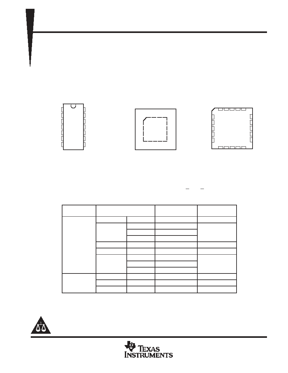
ORDERING INFORMATION
TA
PACKAGE
ORDERABLE
PART NUMBER
TOP-SIDE
MARKING
QFN - RGY
Reel of 1000
SN74LVC86ARGYR
LC86A
Tube of 50
SN74LVC86AD
SOIC - D
Reel of 2500
SN74LVC86ADR
LVC86A
SOIC - D
Reel of 250
SN74LVC86ADT
LVC86A
-40
∞
C to 85
∞
C
SOP - NS
Reel of 2000
SN74LVC86ANSR
LVC86A
-40 C to 85 C
SSOP - DB
Reel of 2000
SN74LVC86ADBR
LC86A
Tube of 90
SN74LVC86APW
TSSOP - PW
Reel of 2000
SN74LVC86APWR
LC86A
TSSOP - PW
Reel of 250
SN74LVC86APWT
LC86A
CDIP - J
Tube of 25
SNJ54LVC86AJ
SNJ54LVC86AJ
-55
∞
C to 125
∞
C
CFP - W
Tube of 150
SNJ54LVC86AW
SNJ54LVC86AW
-55 C to 125 C
LCCC - FK
Tube of 55
SNJ54LVC86AFK
SNJ54LVC86AFK
Package drawings, standard packing quantities, thermal data, symbolization, and PCB design guidelines
are available at www.ti.com/sc/package.
Copyright
2003, Texas Instruments Incorporated
PRODUCTION DATA information is current as of publication date.
Products conform to specifications per the terms of Texas Instruments
standard warranty. Production processing does not necessarily include
testing of all parameters.
Please be aware that an important notice concerning availability, standard warranty, and use in critical applications of
Texas Instruments semiconductor products and disclaimers thereto appears at the end of this data sheet.
SN54LVC86A . . . J OR W PACKAGE
SN74LVC86A . . . D, DB, NS, OR PW PACKAGE
(TOP VIEW)
1
2
3
4
5
6
7
14
13
12
11
10
9
8
1A
1B
1Y
2A
2B
2Y
GND
V
CC
4B
4A
4Y
3B
3A
3Y
3
2 1 20 19
9 10 11 12 13
4
5
6
7
8
18
17
16
15
14
4A
NC
4Y
NC
3B
1Y
NC
2A
NC
2B
1B
1A
NC
3Y
3A
V
4B
2Y
GND
NC
SN54LVC86A . . . FK PACKAGE
(TOP VIEW)
CC
NC - No internal connection
SN74LVC86A . . . RGY PACKAGE
(TOP VIEW)
1
14
7
8
2
3
4
5
6
13
12
11
10
9
4B
4A
4Y
3B
3A
1B
1Y
2A
2B
2Y
1A
3Y
V
GND
CC
On products compliant to MIL PRF 38535, all parameters are tested
unless otherwise noted. On all other products, production
processing does not necessarily include testing of all parameters.
SN54LVC86A, SN74LVC86A
QUADRUPLE 2 INPUT EXCLUSIVE OR GATES
SCAS288O - JANUARY 1993 - REVISED JULY 2003
2
POST OFFICE BOX 655303
∑
DALLAS, TEXAS 75265
description/ordering information (continued)
A common application is as a true/complement element. If one of the inputs is low, the other input is reproduced
in true form at the output. If one of the inputs is high, the signal on the other input is reproduced inverted at
the output.
Inputs can be driven from either 3.3-V or 5-V devices. This feature allows the use of these devices as translators
in a mixed 3.3-V/5-V system environment.
FUNCTION TABLE
(each gate)
INPUTS
OUTPUT
A
B
OUTPUT
Y
L
L
L
L
H
H
H
L
H
H
H
L
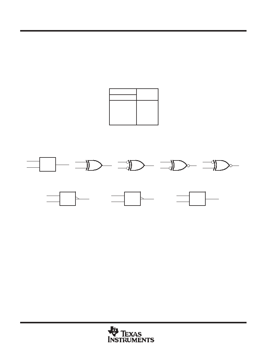
exclusive-OR logic
An exclusive-OR gate has many applications, some of which can be represented better by alternative logic
symbols.
= 1
EXCLUSIVE OR
These five equivalent exclusive-OR symbols are valid for an SN74LVC86A gate in positive logic; negation may be shown at any two ports.
=
2k
2k + 1
LOGIC-IDENTITY ELEMENT
EVEN-PARITY ELEMENT
ODD-PARITY ELEMENT
The output is active (low) if
all inputs stand at the same
logic level (i.e., A = B).
The output is active (low) if
an even number of inputs
(i.e., 0 or 2) are active.
The output is active (high) if
an odd number of inputs
(i.e., only 1 of the 2) are
active.
SN54LVC86A, SN74LVC86A
QUADRUPLE 2 INPUT EXCLUSIVE OR GATES
SCAS288O - JANUARY 1993 - REVISED JULY 2003
3
POST OFFICE BOX 655303
∑
DALLAS, TEXAS 75265
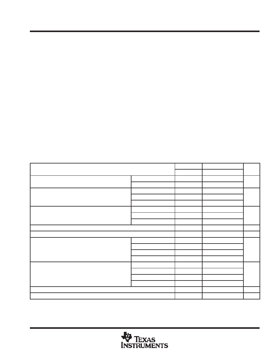
absolute maximum ratings over operating free-air temperature range (unless otherwise noted)
Supply voltage range, V
CC
-0.5 V to 6.5 V
. . . . . . . . . . . . . . . . . . . . . . . . . . . . . . . . . . . . . . . . . . . . . . . . . . . . . . . . .
Input voltage range, V
I
(see Note 1)
-0.5 V to 6.5 V
. . . . . . . . . . . . . . . . . . . . . . . . . . . . . . . . . . . . . . . . . . . . . . . . .
Output voltage range, V
O
(see Notes 1 and 2)
-0.5 V to V
CC
+ 0.5 V
. . . . . . . . . . . . . . . . . . . . . . . . . . . . . . . . . .
Input clamp current, I
IK
(V
I
< 0)
-50 mA
. . . . . . . . . . . . . . . . . . . . . . . . . . . . . . . . . . . . . . . . . . . . . . . . . . . . . . . . . . .
Output clamp current, I
OK
(V
O
< 0)
-50 mA
. . . . . . . . . . . . . . . . . . . . . . . . . . . . . . . . . . . . . . . . . . . . . . . . . . . . . . . .
Continuous output current, I
O
±
50 mA
. . . . . . . . . . . . . . . . . . . . . . . . . . . . . . . . . . . . . . . . . . . . . . . . . . . . . . . . . . . . .
Continuous current through V
CC
or GND
±
100 mA
. . . . . . . . . . . . . . . . . . . . . . . . . . . . . . . . . . . . . . . . . . . . . . . . . .
Package thermal impedance,
JA
(see Note 3): D package
86
∞
C/W
. . . . . . . . . . . . . . . . . . . . . . . . . . . . . . . . . . .
(see Note 3): DB package
96
∞
C/W
. . . . . . . . . . . . . . . . . . . . . . . . . . . . . . . . .
(see Note 3): NS package
76
∞
C/W
. . . . . . . . . . . . . . . . . . . . . . . . . . . . . . . . .
(see Note 3): PW package
113
∞
C/W
. . . . . . . . . . . . . . . . . . . . . . . . . . . . . . . .
(see Note 4): RGY package
47
∞
C/W
. . . . . . . . . . . . . . . . . . . . . . . . . . . . . . . .
Storage temperature range, T
stg
-65
∞
C to 150
∞
C
. . . . . . . . . . . . . . . . . . . . . . . . . . . . . . . . . . . . . . . . . . . . . . . . . . .
Stresses beyond those listed under "absolute maximum ratings" may cause permanent damage to the device. These are stress ratings only, and
functional operation of the device at these or any other conditions beyond those indicated under "recommended operating conditions" is not
implied. Exposure to absolute-maximum-rated conditions for extended periods may affect device reliability.
NOTES:
1. The input negative-voltage and output voltage ratings may be exceeded if the input and output current ratings are observed.
2. The value of VCC is provided in the recommended operating conditions table.
3. The package thermal impedance is calculated in accordance with JESD 51-7.
4. The package thermal impedance is calculated in accordance with JESD 51-5.
recommended operating conditions (see Note 5)
SN54LVC86A
SN74LVC86A
UNIT
MIN
MAX
MIN
MAX
UNIT
VCC
Supply voltage
Operating
2
3.6
1.65
3.6
V
VCC
Supply voltage
Data retention only
1.5
1.5
V
VCC = 1.65 V to 1.95 V
0.65
◊
VCC
VIH
High-level input voltage
VCC = 2.3 V to 2.7 V
1.7
V
VIH
High-level input voltage
VCC = 2.7 V to 3.6 V
2
2
V
VCC = 1.65 V to 1.95 V
0.35
◊
VCC
VIL
Low-level input voltage
VCC = 2.3 V to 2.7 V
0.7
V
VIL
Low-level input voltage
VCC = 2.7 V to 3.6 V
0.8
0.8
V
VI
Input voltage
0
5.5
0
5.5
V
VO
Output voltage
0
VCC
0
VCC
V
VCC = 1.65 V
-4
IOH
High-level output current
VCC = 2.3 V
-8
mA
IOH
High-level output current
VCC = 2.7 V
-12
-12
mA
VCC = 3 V
-24
-24
VCC = 1.65 V
4
IOL
Low-level output current
VCC = 2.3 V
8
mA
IOL
Low-level output current
VCC = 2.7 V
12
12
mA
VCC = 3 V
24
24
t/
v
Input transition rise or fall rate
9
9
ns/V
TA
Operating free-air temperature
-55
125
-40
85
∞
C
NOTE 5: All unused inputs of the device must be held at VCC or GND to ensure proper device operation. Refer to the TI application report,
Implications of Slow or Floating CMOS Inputs, literature number SCBA004.
SN54LVC86A, SN74LVC86A
QUADRUPLE 2 INPUT EXCLUSIVE OR GATES
SCAS288O - JANUARY 1993 - REVISED JULY 2003
4
POST OFFICE BOX 655303
∑
DALLAS, TEXAS 75265
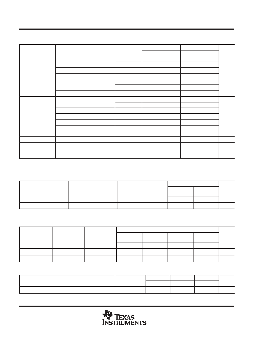
electrical characteristics over recommended operating free-air temperature range (unless
otherwise noted)
PARAMETER
TEST CONDITIONS
VCC
SN54LVC86A
SN74LVC86A
UNIT
PARAMETER
TEST CONDITIONS
VCC
MIN
TYP
MAX
MIN
TYP
MAX
UNIT
IOH = -100 A
1.65 V to 3.6 V
VCC-0.2
IOH = -100
µ
A
2.7 V to 3.6 V
VCC-0.2
IOH = -4 mA
1.65 V
1.2
VOH
IOH = -8 mA
2.3 V
1.7
V
VOH
IOH = -12 mA
2.7 V
2.2
2.2
V
IOH = -12 mA
3 V
2.4
2.4
IOH = -24 mA
3 V
2.2
2.2
IOL = 100 A
1.65 V to 3.6 V
0.2
IOL = 100
µ
A
2.7 V to 3.6 V
0.2
VOL
IOL = 4 mA
1.65 V
0.45
V
VOL
IOL = 8 mA
2.3 V
0.7
V
IOL = 12 mA
2.7 V
0.4
0.4
IOL = 24 mA
3 V
0.55
0.55
II
VI = 5.5 V or GND
3.6 V
±
5
±
5
µ
A
ICC
VI = VCC or GND,
IO = 0
3.6 V
10
10
µ
A
ICC
One input at VCC - 0.6 V,
Other inputs at VCC or GND
2.7 V to 3.6 V
500
500
µ
A
Ci
VI = VCC or GND
3.3 V
5
5
pF
All typical values are at VCC = 3.3 V, TA = 25
∞
C.
switching characteristics over recommended operating free-air temperature range (unless
otherwise noted) (see Figure 1)
SN54LVC86A
PARAMETER
FROM
(INPUT)
TO
(OUTPUT)
VCC = 2.7 V
VCC = 3.3 V
±
0.3 V
UNIT
(INPUT)
(OUTPUT)
MIN
MAX
MIN
MAX
tpd
A
Y
5.6
1
4.6
ns
switching characteristics over recommended operating free-air temperature range (unless
otherwise noted) (see Figure 1)
SN74LVC86A
PARAMETER
FROM
(INPUT)
TO
(OUTPUT)
VCC = 1.8 V
±
0.15 V
VCC = 2.5 V
±
0.2 V
VCC = 2.7 V
VCC = 3.3 V
±
0.3 V
UNIT
(INPUT)
(OUTPUT)
MIN
MAX
MIN
MAX
MIN
MAX
MIN
MAX
tpd
A
Y
1
9.9
1
7.6
1
5.6
1
4.6
ns
tsk(o)
1
ns
operating characteristics, T
A
= 25
∞
C
PARAMETER
TEST
VCC = 1.8 V
VCC = 2.5 V
VCC = 3.3 V
UNIT
PARAMETER
TEST
CONDITIONS
TYP
TYP
TYP
UNIT
Cpd
Power dissipation capacitance per gate
f = 10 MHz
6.5
7.5
8.5
pF
SN54LVC86A, SN74LVC86A
QUADRUPLE 2 INPUT EXCLUSIVE OR GATES
SCAS288O - JANUARY 1993 - REVISED JULY 2003
5
POST OFFICE BOX 655303
∑
DALLAS, TEXAS 75265
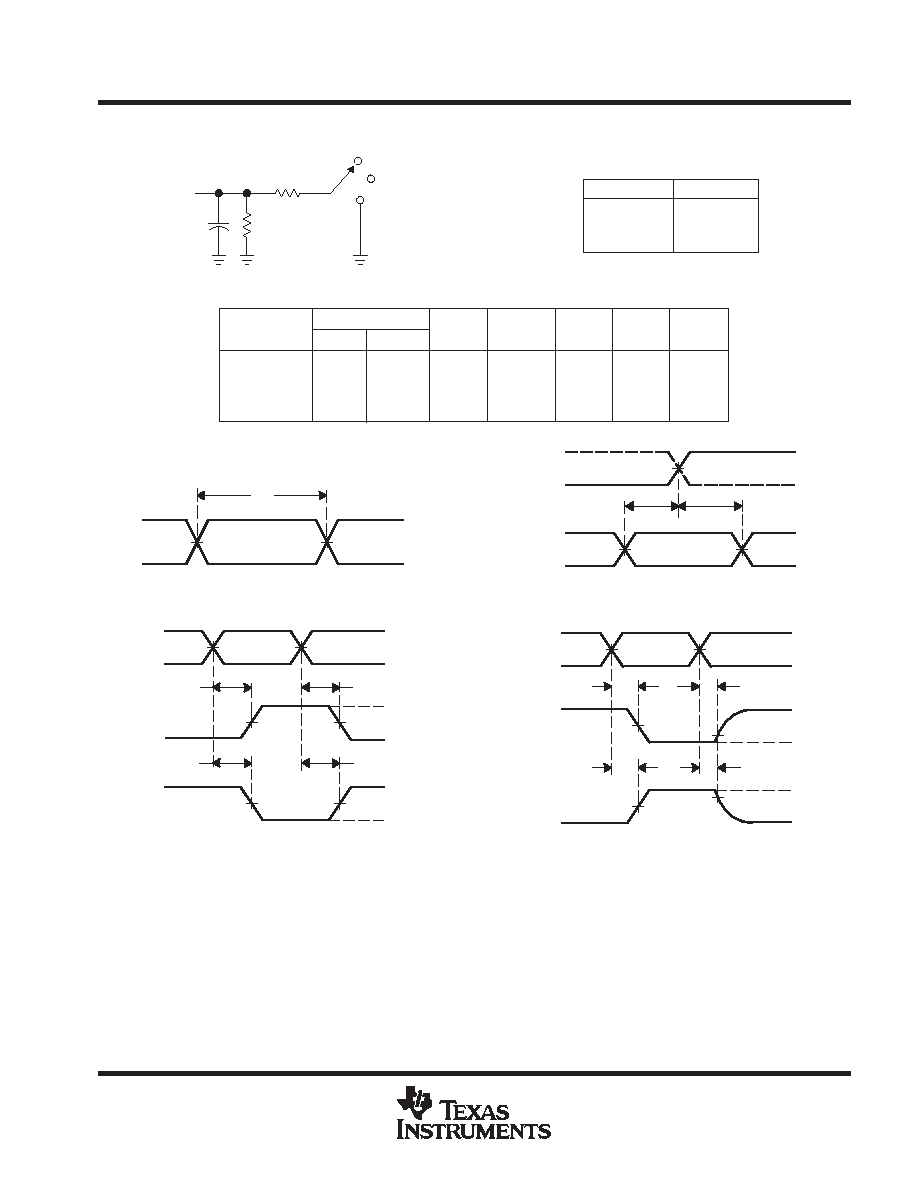
PARAMETER MEASUREMENT INFORMATION
VM
th
tsu
From Output
Under Test
CL
(see Note A)
LOAD CIRCUIT
S1
VLOAD
Open
GND
RL
RL
Data Input
Timing Input
VI
0 V
VI
0 V
0 V
tw
Input
VOLTAGE WAVEFORMS
SETUP AND HOLD TIMES
VOLTAGE WAVEFORMS
PROPAGATION DELAY TIMES
INVERTING AND NONINVERTING OUTPUTS
VOLTAGE WAVEFORMS
PULSE DURATION
tPLH
tPHL
tPHL
tPLH
VOH
VOH
VOL
VOL
VI
0 V
Input
Output
Waveform 1
S1 at VLOAD
(see Note B)
Output
Waveform 2
S1 at GND
(see Note B)
VOL
VOH
tPZL
tPZH
tPLZ
tPHZ
VLOAD/2
0 V
VOL + V
VOH - V
0 V
VI
VOLTAGE WAVEFORMS
ENABLE AND DISABLE TIMES
LOW- AND HIGH-LEVEL ENABLING
Output
Output
tPLH/tPHL
tPLZ/tPZL
tPHZ/tPZH
Open
VLOAD
GND
TEST
S1
NOTES: A. CL includes probe and jig capacitance.
B. Waveform 1 is for an output with internal conditions such that the output is low except when disabled by the output control.
Waveform 2 is for an output with internal conditions such that the output is high except when disabled by the output control.
C. All input pulses are supplied by generators having the following characteristics: PRR
10 MHz, ZO = 50
.
D. The outputs are measured one at a time with one transition per measurement.
E. tPLZ and tPHZ are the same as tdis.
F. tPZL and tPZH are the same as ten.
G. tPLH and tPHL are the same as tpd.
H. All parameters and waveforms are not applicable to all devices.
Output
Control
VM
VM
VM
VM
VM
VM
VM
VM
VM
VM
VM
VM
VI
VM
VM
1.8 V
±
0.15 V
2.5 V
±
0.2 V
2.7 V
3.3 V
±
0.3 V
1 k
500
500
500
VCC
RL
2
◊
VCC
2
◊
VCC
6 V
6 V
VLOAD
CL
30 pF
30 pF
50 pF
50 pF
0.15 V
0.15 V
0.3 V
0.3 V
V
VCC
VCC
2.7 V
2.7 V
VI
VCC/2
VCC/2
1.5 V
1.5 V
VM
tr/tf
2 ns
2 ns
2.5 ns
2.5 ns
INPUTS
Figure 1. Load Circuit and Voltage Waveforms