
SN54AHC138, SN74AHC138
3-LINE TO 8-LINE DECODERS/DEMULTIPLEXERS
SCLS258L ≠ DECEMBER 1995 ≠ REVISED JULY 2003
1
POST OFFICE BOX 655303
∑
DALLAS, TEXAS 75265
D
Operating Range 2-V to 5.5-V V
CC
D
Designed Specifically for High-Speed
Memory Decoders and Data-Transmission
Systems
D
Incorporate Three Enable Inputs to Simplify
Cascading and/or Data Reception
D
Latch-Up Performance Exceeds 250 mA Per
JESD 17
D
ESD Protection Exceeds JESD 22
≠ 2000-V Human-Body Model (A114-A)
≠ 200-V Machine Model (A115-A)
≠ 1000-V Charged-Device Model (C101)
3
2 1 20 19
9 10 11 12 13
4
5
6
7
8
18
17
16
15
14
Y1
Y2
NC
Y3
Y4
C
G2A
NC
G2B
G1
B
A
NC
Y6
Y5
V
Y0
Y7
GND
NC
SN54AHC138 . . . FK PACKAGE
(TOP VIEW)
CC
NC ≠ No internal connection
1
2
3
4
5
6
7
8
16
15
14
13
12
11
10
9
A
B
C
G2A
G2B
G1
Y7
GND
V
CC
Y0
Y1
Y2
Y3
Y4
Y5
Y6
SN54AHC138 . . . J OR W PACKAGE
SN74AHC138 . . . D, DB, DGV, N, NS,
OR PW PACKAGE
(TOP VIEW)
SN74AHC138 . . . RGY PACKAGE
(TOP VIEW)
1
16
8
9
2
3
4
5
6
7
15
14
13
12
11
10
Y0
Y1
Y2
Y3
Y4
Y5
B
C
G2A
G2B
G1
Y7
A
Y6
V
GND
CC
description/ordering information
The 'AHC138 decoders/demultiplexers are designed for high-performance memory-decoding and data-routing
applications that require very short propagation-delay times. In high-performance memory systems, these
decoders can be used to minimize the effects of system decoding. When employed with high-speed memories
utilizing a fast enable circuit, the delay times of these decoders and the enable time of the memory usually are
less than the typical access time of the memory. This means that the effective system delay introduced by the
decoders is negligible.
ORDERING INFORMATION
TA
PACKAGE
ORDERABLE
PART NUMBER
TOP-SIDE
MARKING
QFN ≠ RGY
Tape and reel
SN74AHC138RGYR
HA138
PDIP ≠ N
Tube
SN74AHC138N
SN74AHC138N
SOIC ≠ D
Tube
SN74AHC138D
AHC138
SOIC ≠ D
Tape and reel
SN74AHC138DR
AHC138
≠40
∞
C to 85
∞
C
SOP ≠ NS
Tape and reel
SN74AHC138NSR
AHC138
SSOP ≠ DB
Tape and reel
SN74AHC138DBR
HA138
TSSOP
PW
Tube
SN74AHC138PW
HA138
TSSOP ≠ PW
Tape and reel
SN74AHC138PWR
HA138
TVSOP ≠ DGV
Tape and reel
SN74AHC138DGVR
HA138
CDIP ≠ J
Tube
SNJ54AHC138J
SNJ54AHC138J
≠55
∞
C to 125
∞
C
CFP ≠ W
Tube
SNJ54AHC138W
SNJ54AHC138W
LCCC ≠ FK
Tube
SNJ54AHC138FK
SNJ54AHC138FK
Package drawings, standard packing quantities, thermal data, symbolization, and PCB design guidelines
are available at www.ti.com/sc/package.
On products compliant to MIL-PRF-38535, all parameters are tested
unless otherwise noted. On all other products, production
processing does not necessarily include testing of all parameters.
Copyright
2003, Texas Instruments Incorporated
PRODUCTION DATA information is current as of publication date.
Products conform to specifications per the terms of Texas Instruments
standard warranty. Production processing does not necessarily include
testing of all parameters.
Please be aware that an important notice concerning availability, standard warranty, and use in critical applications of
Texas Instruments semiconductor products and disclaimers thereto appears at the end of this data sheet.

SN54AHC138, SN74AHC138
3-LINE TO 8-LINE DECODERS/DEMULTIPLEXERS
SCLS258L ≠ DECEMBER 1995 ≠ REVISED JULY 2003
2
POST OFFICE BOX 655303
∑
DALLAS, TEXAS 75265
description/ordering information (continued)
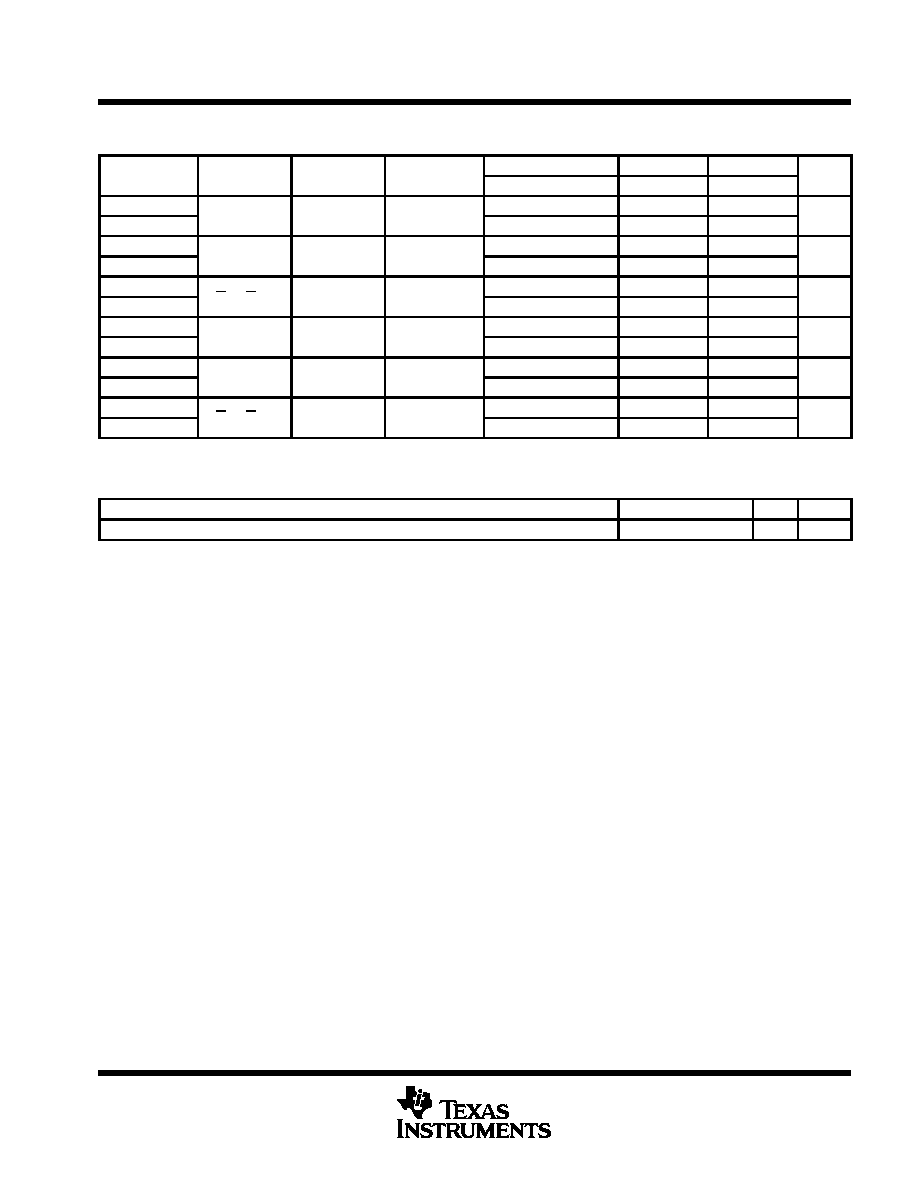
The conditions at the binary-select inputs and the three enable inputs select one of eight output lines. Two
active-low and one active-high enable inputs reduce the need for external gates or inverters when expanding.
A 24-line decoder can be implemented without external inverters, and a 32-line decoder requires only one
inverter. An enable input can be used as a data input for demultiplexing applications.
FUNCTION TABLE
ENABLE INPUTS
SELECT INPUTS
OUTPUTS
G1
G2A
G2B
C
B
A
Y0
Y1
Y2
Y3
Y4
Y5
Y6
Y7
X
H
X
X
X
X
H
H
H
H
H
H
H
H
X
X
H
X
X
X
H
H
H
H
H
H
H
H
L
X
X
X
X
X
H
H
H
H
H
H
H
H
H
L
L
L
L
L
L
H
H
H
H
H
H
H
H
L
L
L
L
H
H
L
H
H
H
H
H
H
H
L
L
L
H
L
H
H
L
H
H
H
H
H
H
L
L
L
H
H
H
H
H
L
H
H
H
H
H
L
L
H
L
L
H
H
H
H
L
H
H
H
H
L
L
H
L
H
H
H
H
H
H
L
H
H
H
L
L
H
H
L
H
H
H
H
H
H
L
H
H
L
L
H
H
H
H
H
H
H
H
H
H
L
logic diagram (positive logic)
G1
G2B
G2A
C
B
A
Y7
Y6
Y5
Y4
Y3
Y2
Y1
Y0
Data
Outputs
Select
Inputs
Enable
Inputs
1
2
3
4
5
6
15
14
13
12
11
10
9
7
Pin numbers shown are for the D, DB, DGV, J, N, NS, PW, RGY, and W packages.

SN54AHC138, SN74AHC138
3-LINE TO 8-LINE DECODERS/DEMULTIPLEXERS
SCLS258L ≠ DECEMBER 1995 ≠ REVISED JULY 2003
3
POST OFFICE BOX 655303
∑
DALLAS, TEXAS 75265
absolute maximum ratings over operating free-air temperature range (unless otherwise noted)
Supply voltage range, V
CC
≠0.5 V to 7 V
. . . . . . . . . . . . . . . . . . . . . . . . . . . . . . . . . . . . . . . . . . . . . . . . . . . . . . . . . .
Input voltage range, V
I
(see Note 1)
≠0.5 V to 7 V
. . . . . . . . . . . . . . . . . . . . . . . . . . . . . . . . . . . . . . . . . . . . . . . . . .
Output voltage range, V
O
(see Note 1)
≠0.5 V to V
CC
+ 0.5 V
. . . . . . . . . . . . . . . . . . . . . . . . . . . . . . . . . . . . . . . .
Input clamp current, I
IK
(V
I
< 0)
≠20 mA
. . . . . . . . . . . . . . . . . . . . . . . . . . . . . . . . . . . . . . . . . . . . . . . . . . . . . . . . . . .
Output clamp current, I
OK
(V
O
< 0 or V
O
> V
CC
)
±
20 mA
. . . . . . . . . . . . . . . . . . . . . . . . . . . . . . . . . . . . . . . . . . . .
Continuous output current, I
O
(V
O
= 0 to V
CC
)
±
25 mA
. . . . . . . . . . . . . . . . . . . . . . . . . . . . . . . . . . . . . . . . . . . . . .
Continuous current through V
CC
or GND
±
75 mA
. . . . . . . . . . . . . . . . . . . . . . . . . . . . . . . . . . . . . . . . . . . . . . . . . . .
Package thermal impedance,
JA
(see Note 2): D package
73
∞
C/W
. . . . . . . . . . . . . . . . . . . . . . . . . . . . . . . . . . .
(see Note 2): DB package
82
∞
C/W
. . . . . . . . . . . . . . . . . . . . . . . . . . . . . . . . .
(see Note 2): DGV package
120
∞
C/W
. . . . . . . . . . . . . . . . . . . . . . . . . . . . . . .
(see Note 2): N package
67
∞
C/W
. . . . . . . . . . . . . . . . . . . . . . . . . . . . . . . . . . .
(see Note 2): NS package
64
∞
C/W
. . . . . . . . . . . . . . . . . . . . . . . . . . . . . . . . .
(see Note 2): PW package
108
∞
C/W
. . . . . . . . . . . . . . . . . . . . . . . . . . . . . . . .
(see Note 3): RGY package
39
∞
C/W
. . . . . . . . . . . . . . . . . . . . . . . . . . . . . . . .
Storage temperature range, T
stg
≠65
∞
C to 150
∞
C
. . . . . . . . . . . . . . . . . . . . . . . . . . . . . . . . . . . . . . . . . . . . . . . . . . .
Stresses beyond those listed under "absolute maximum ratings" may cause permanent damage to the device. These are stress ratings only, and
functional operation of the device at these or any other conditions beyond those indicated under "recommended operating conditions" is not
implied. Exposure to absolute-maximum-rated conditions for extended periods may affect device reliability.
NOTES:
1. The input and output voltage ratings may be exceeded if the input and output current ratings are observed.
2. The package thermal impedance is calculated in accordance with JESD 51-7.
3. The package thermal impedance is calculated in accordance with JESD 51-5.
recommended operating conditions (see Note 4)
SN54AHC138
SN74AHC138
UNIT
MIN
MAX
MIN
MAX
UNIT
VCC
Supply voltage
2
5.5
2
5.5
V
VCC = 2 V
1.5
1.5
VIH
High-level input voltage
VCC = 3 V
2.1
2.1
V
VCC = 5.5 V
3.85
3.85
VCC = 2 V
0.5
0.5
VIL
Low-level input voltage
VCC = 3 V
0.9
0.9
V
VCC = 5.5 V
1.65
1.65
VI
Input voltage
0
5.5
0
5.5
V
VO
Output voltage
0
VCC
0
VCC
V
VCC = 2 V
≠50
≠50
m
A
IOH
High-level output current
VCC = 3.3 V
±
0.3 V
≠4
≠4
mA
VCC = 5 V
±
0.5 V
≠8
≠8
mA
VCC = 2 V
50
50
m
A
IOL
Low-level output current
VCC = 3.3 V
±
0.3 V
4
4
mA
VCC = 5 V
±
0.5 V
8
8
mA
t/
v
Input transition rise or fall rate
VCC = 3.3 V
±
0.3 V
100
100
ns/V
t/
v
Input transition rise or fall rate
VCC = 5 V
±
0.5 V
20
20
ns/V
TA
Operating free-air temperature
≠55
125
≠40
85
∞
C
NOTE 4: All unused inputs of the device must be held at VCC or GND to ensure proper device operation. Refer to the TI application report,
Implications of Slow or Floating CMOS Inputs, literature number SCBA004.

SN54AHC138, SN74AHC138
3-LINE TO 8-LINE DECODERS/DEMULTIPLEXERS
SCLS258L ≠ DECEMBER 1995 ≠ REVISED JULY 2003
4
POST OFFICE BOX 655303
∑
DALLAS, TEXAS 75265
electrical characteristics over recommended operating free-air temperature range (unless
otherwise noted)
PARAMETER
TEST CONDITIONS
VCC
TA = 25
∞
C
SN54AHC138
SN74AHC138
UNIT
PARAMETER
TEST CONDITIONS
VCC
MIN
TYP
MAX
MIN
MAX
MIN
MAX
UNIT
2 V
1.9
2
1.9
1.9
IOH = ≠50
m
A
3 V
2.9
3
2.9
2.9
VOH
4.5 V
4.4
4.5
4.4
4.4
V
OH
IOH = ≠4 mA
3 V
2.58
2.48
2.48
IOH = ≠8 mA
4.5 V
3.94
3.8
3.8
2 V
0.1
0.1
0.1
IOL = 50
m
A
3 V
0.1
0.1
0.1
VOL
4.5 V
0.1
0.1
0.1
V
OL
IOL = 4 mA
3 V
0.36
0.5
0.44
IOL = 8 mA
4.5 V
0.36
0.5
0.44
II
VI = 5.5 V or GND
0 V to 5.5 V
±
0.1
±
1*
±
1
m
A
ICC
VI = VCC or GND,
IO = 0
5.5 V
4
40
40
m
A
Ci
VI = VCC or GND
5 V
2
10
10
pF
* On products compliant to MIL-PRF-38535, this parameter is not production tested at VCC = 0 V.
switching characteristics over recommended operating free-air temperature range,
V
CC
= 3.3 V
±
0.3 V (unless otherwise noted) (see Figure 1)
PARAMETER
FROM
TO
LOAD
TA = 25
∞
C
SN54AHC138
SN74AHC138
UNIT
PARAMETER
(INPUT)
(OUTPUT)
CAPACITANCE
MIN
TYP
MAX
MIN
MAX
MIN
MAX
UNIT
tPLH
A B C
Any Y
CL = 15 pF
8.2**
11.4**
1**
13**
1
13
ns
tPHL
A, B, C
Any Y
CL = 15 pF
8.2**
11.4**
1**
13**
1
13
ns
tPLH
G1
Any Y
CL = 15 pF
8.1**
12.8**
1**
15**
1
15
ns
tPHL
G1
Any Y
CL = 15 pF
8.1**
12.8**
1**
15**
1
15
ns
tPLH
G2A G2B
Any Y
CL = 15 pF
8.2**
11.4**
1**
13.5**
1
13.5
ns
tPHL
G2A, G2B
Any Y
CL = 15 pF
8.2**
11.4**
1**
13.5**
1
13.5
ns
tPLH
A B C
Any Y
CL = 50 pF
10
15.8
1
18
1
18
ns
tPHL
A, B, C
Any Y
CL = 50 pF
10
15.8
1
18
1
18
ns
tPLH
G1
Any Y
CL = 50 pF
10.6
16.3
1
18.5
1
18.5
ns
tPHL
G1
Any Y
CL = 50 pF
10.6
16.3
1
18.5
1
18.5
ns
tPLH
G2A G2B
Any Y
CL = 50 pF
10.7
14.9
1
17
1
17
ns
tPHL
G2A, G2B
Any Y
CL = 50 pF
10.7
14.9
1
17
1
17
ns
** On products compliant to MIL-PRF-38535, this parameter is not production tested.
SN54AHC138, SN74AHC138
3-LINE TO 8-LINE DECODERS/DEMULTIPLEXERS
SCLS258L ≠ DECEMBER 1995 ≠ REVISED JULY 2003
5
POST OFFICE BOX 655303
∑
DALLAS, TEXAS 75265
switching characteristics over recommended operating free-air temperature range,
V
CC
= 5 V
±
0.5 V (unless otherwise noted) (see Figure 1)
PARAMETER
FROM
TO
LOAD
TA = 25
∞
C
SN54AHC138
SN74AHC138
UNIT
PARAMETER
(INPUT)
(OUTPUT)
CAPACITANCE
MIN
TYP
MAX
MIN
MAX
MIN
MAX
UNIT
tPLH
A B C
Any Y
CL = 15 pF
5.7*
8.1*
1*
9.5*
1
9.5
ns
tPHL
A, B, C
Any Y
CL = 15 pF
5.7*
8.1*
1*
9.5*
1
9.5
ns
tPLH
G1
Any Y
CL = 15 pF
5.6*
8.1*
1*
9.5*
1
9.5
ns
tPHL
G1
Any Y
CL = 15 pF
5.6*
8.1*
1*
9.5*
1
9.5
ns
tPLH
G2A G2B
Any Y
CL = 15 pF
5.8*
8.1*
1*
9.5*
1
9.5
ns
tPHL
G2A, G2B
Any Y
CL = 15 pF
5.8*
8.1*
1*
9.5*
1
9.5
ns
tPLH
A B C
Any Y
CL = 50 pF
7.2
10.1
1
11.5
1
11.5
ns
tPHL
A, B, C
Any Y
CL = 50 pF
7.2
10.1
1
11.5
1
11.5
ns
tPLH
G1
Any Y
CL = 50 pF
7.1
10.1
1
11.5
1
11.5
ns
tPHL
G1
Any Y
CL = 50 pF
7.1
10.1
1
11.5
1
11.5
ns
tPLH
G2A G2B
Any Y
CL = 50 pF
7.3
10.1
1
11.5
1
11.5
ns
tPHL
G2A, G2B
Any Y
CL = 50 pF
7.3
10.1
1
11.5
1
11.5
ns
* On products compliant to MIL-PRF-38535, this parameter is not production tested.
operating characteristics, V
CC
= 5 V, T
A
= 25
∞
C
PARAMETER
TEST CONDITIONS
TYP
UNIT
Cpd
Power dissipation capacitance
No load,
f = 1 MHz
13
pF