"SM320C6201B,SMJ320C6201B Digital Signal Processor"
SM320C6201B, SMJ320C6201B
DIGITAL SIGNAL PROCESSOR
SGUS031B APRIL 2000 REVISED AUGUST 2001
1
POST OFFICE BOX 1443
·
HOUSTON, TEXAS 772511443
D
Highest Performance Fixed-Point Digital
Signal Processor (DSP) SM/SMJ320C6201B
5-, 6.7-ns Instruction Cycle Time
150 and 200-MHz Clock Rate
Eight 32-Bit Instructions/Cycle
1200 and 1600 MIPS
D
VelociTI
Advanced Very Long Instruction
Word (VLIW) C62x
CPU Core
Eight Independent Functional Units:
Six ALUs (32-/40-Bit)
Two 16-Bit Multipliers (32-Bit Results)
Load-Store Architecture With 32 32-Bit
General-Purpose Registers
Instruction Packing Reduces Code Size
All Instructions Conditional
D
Instruction Set Features
Byte-Addressable (8-, 16-, 32-Bit Data)
32-Bit Address Range
8-Bit Overflow Protection
Saturation
Bit-Field Extract, Set, Clear
Bit-Counting
Normalization
D
1M-Bit On-Chip SRAM
512K-Bit Internal Program/Cache
(16K 32-Bit Instructions)
512K-Bit Dual-Access Internal Data
(64K Bytes) Organized as Two Blocks for
Improved Concurrency
D
32-Bit External Memory Interface (EMIF)
Glueless Interface to Synchronous
Memories: SDRAM and SBSRAM
Glueless Interface to Asynchronous
Memories: SRAM and EPROM
D
Four-Channel Bootloading
Direct-Memory-Access (DMA) Controller
with an Auxiliary Channel
D
16-Bit Host-Port Interface (HPI)
Access to Entire Memory Map
D
Two Multichannel Buffered Serial Ports
(McBSPs)
Direct Interface to T1/E1, MVIP, SCSA
Framers
ST-Bus-Switching Compatible
Up to 256 Channels Each
AC97-Compatible
Serial Peripheral Interface (SPI)
Compatible (Motorola
)
D
Two 32-Bit General-Purpose Timers
D
Flexible Phase-Locked Loop (PLL) Clock
Generator
D
IEEE-1149.1 (JTAG
) Boundary-Scan
Compatible
D
429-Pin BGA Package (GLP Suffix)
D
CMOS Technology
0.18-
µ
m/5-Level Metal Process
D
3.3-V I/Os, 1.8-V Internal
Please be aware that an important notice concerning availability, standard warranty, and use in critical applications of
Texas Instruments semiconductor products and disclaimers thereto appears at the end of this data sheet.
C62x and VelociTI are trademarks of Texas Instruments Incorporated.
Motorola is a trademark of Motorola, Inc.
IEEE Standard 1149.1-1990 Standard-Test-Access Port and Boundary Scan Architecture.
Copyright
2001, Texas Instruments Incorporated
UNLESS OTHERWISE NOTED this document contains PRODUCTION
DATA information current as of publication date. Products conform to
specifications per the terms of Texas Instruments standard warranty.
Production processing does not necessarily include testing of all
parameters.
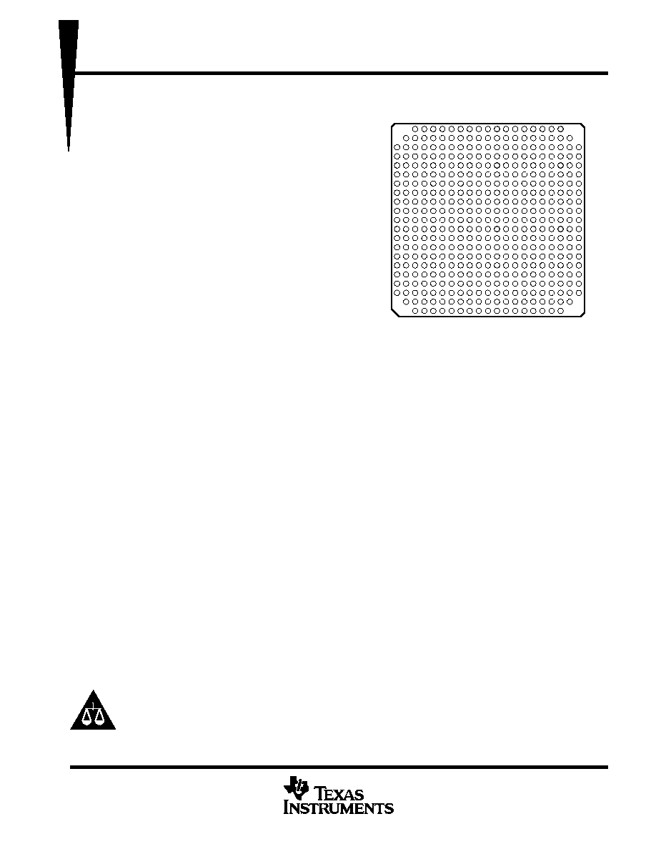
GLP
429-PIN BALL GRID ARRAY (BGA) PACKAGE
(BOTTOM VIEW)
20
21
19
18
16
15
17
13
11
10
12
14
W
Y
AA
V
T
U
P
M
N
R
8
7
6
4
5
L
J
K
G
E
F
H
3
2
D
B
C
A
1
9
On products compliant to MIL PRF 38535, all parameters are tested
unless otherwise noted. On all other products, production
processing does not necessarily include testing of all parameters.
SM320C6201B, SMJ320C6201B
DIGITAL SIGNAL PROCESSOR
SGUS031B APRIL 2000 REVISED AUGUST 2001
2
POST OFFICE BOX 1443
·
HOUSTON, TEXAS 772511443
Table of Contents
parameter measurement information
30
. . . . . . . . . . . . . . .
signal transition levels
30
. . . . . . . . . . . . . . . . . . . . . . . . . . . .
input and output clocks
31
. . . . . . . . . . . . . . . . . . . . . . . . . . .
asynchronous memory timing
34
. . . . . . . . . . . . . . . . . . . . .
synchronous-burst memory timing
36
. . . . . . . . . . . . . . . . .
synchronous DRAM timing
40
. . . . . . . . . . . . . . . . . . . . . . . .
HOLD/HOLDA timing
44
. . . . . . . . . . . . . . . . . . . . . . . . . . . .
reset timing
45
. . . . . . . . . . . . . . . . . . . . . . . . . . . . . . . . . . . . .
external interrupt timing
47
. . . . . . . . . . . . . . . . . . . . . . . . . .
host-port interface timing
48
. . . . . . . . . . . . . . . . . . . . . . . . .
multichannel buffered serial port timing
51
. . . . . . . . . . . . .
DMAC, timer, power-down timing
59
. . . . . . . . . . . . . . . . . .
JTAG test-port timing
60
. . . . . . . . . . . . . . . . . . . . . . . . . . . .
mechanical data
61
. . . . . . . . . . . . . . . . . . . . . . . . . . . . . . . . .
description
2
. . . . . . . . . . . . . . . . . . . . . . . . . . . . . . . . . . . . . . . . .
device characteristics
3
. . . . . . . . . . . . . . . . . . . . . . . . . . . . . . . .
functional block diagram
3
. . . . . . . . . . . . . . . . . . . . . . . . . . . . . .
CPU description
4
. . . . . . . . . . . . . . . . . . . . . . . . . . . . . . . . . . . . .
signal groups description
7
. . . . . . . . . . . . . . . . . . . . . . . . . . . . .
signal descriptions
9
. . . . . . . . . . . . . . . . . . . . . . . . . . . . . . . . . . .
development support
22
. . . . . . . . . . . . . . . . . . . . . . . . . . . . . . . .
device and development support nomenclature
23
. . . . . . . . .
documentation support
24
. . . . . . . . . . . . . . . . . . . . . . . . . . . . . .
clock PLL
26
. . . . . . . . . . . . . . . . . . . . . . . . . . . . . . . . . . . . . . . . .
power-supply sequencing
27
. . . . . . . . . . . . . . . . . . . . . . . . . . . .
absolute maximum ratings over operating case
temperature ranges
28
. . . . . . . . . . . . . . . . . . . . . . . . . . . .
recommended operating conditions
28
. . . . . . . . . . . . . . . . . . .
electrical characteristics over recommended ranges of
supply voltage and operating case temperature
29
. . . .
description
The 320C6201B DSP is a member of the fixed-point DSP family in the 320C6000 platform. The
SM/SMJ320C6201B (C6201B) device is based on the high-performance, advanced VelociTI
very-long-instruction-word (VLIW) architecture developed by Texas Instruments (TI
), making this DSP an
excellent choice for multichannel and multifunction applications. With performance of up to 1600 million
instructions per second (MIPS) at a clock rate of 200 MHz, the C6201B offers cost-effective solutions to
high-performance DSP programming challenges. The C6201B is a newer revision of the C6201. The C6201B
DSP possesses the operational flexibility of high-speed controllers and the numerical capability of array
processors. This processor has 32 general-purpose registers of 32-bit word length and eight highly independent
functional units. The eight functional units provide six arithmetic logic units (ALUs) for a high degree of
parallelism and two 16-bit multipliers for a 32-bit result. The C6201B can produce two multiply-accumulates
(MACs) per cycle--for a total of 400 million MACs per second (MMACS). The C6201B DSP also has
application-specific hardware logic, on-chip memory, and additional on-chip peripherals.
The C6201B includes a large bank of on-chip memory and has a powerful and diverse set of peripherals.
Program memory consists of a 64K-byte block that is user-configurable as cache or memory-mapped program
space. Data memory of the C6201B consists of two 32K-byte blocks of RAM for improved concurrency. The
peripheral set includes two multichannel buffered serial ports (McBSPs), two general-purpose timers, a
host-port interface (HPI), and a glueless external memory interface (EMIF) capable of interfacing to SDRAM
or SBSRAM and asynchronous peripherals.
The C6201B has a complete set of development tools which includes: a new C compiler, a third-party Ada 95
compiler, an assembly optimizer to simplify programming and scheduling, and a Windows
debugger interface
for visibility into source code execution.
TI is a trademark of Texas Instruments Incorporated.
Windows is a registered trademark of the Microsoft Corporation.
SM320C6201B, SMJ320C6201B
DIGITAL SIGNAL PROCESSOR
SGUS031B APRIL 2000 REVISED AUGUST 2001
3
POST OFFICE BOX 1443
·
HOUSTON, TEXAS 772511443
device characteristics
Table 1 provides an overview of the C62x DSP. The table shows significant features of each device, including
the capacity of on-chip RAM, the peripherals, the execution time, and the package type with pin count.
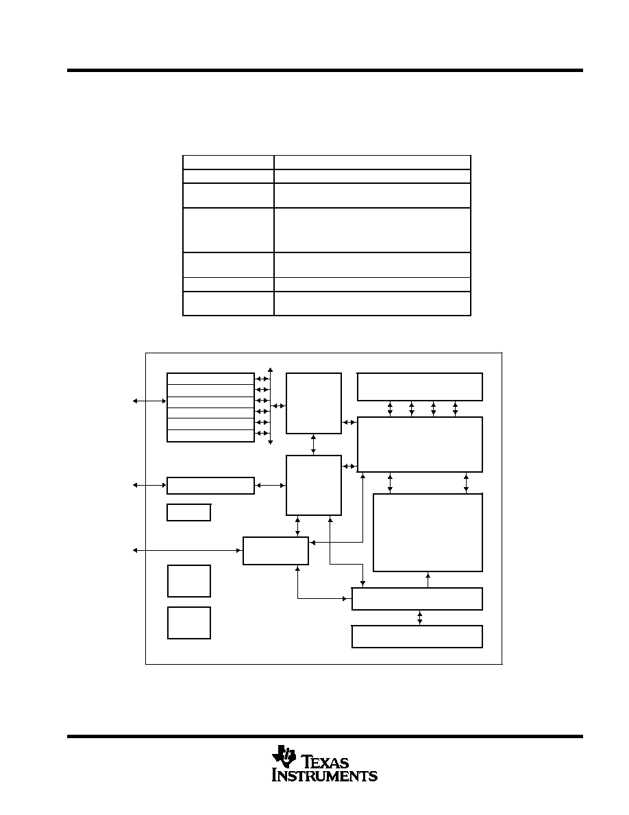
Table 1. Characteristics of the C6201B Processor
CHARACTERISTICS
DESCRIPTION
Device Number
320C6201B
On-Chip Memory
512-Kbit Program Memory
512-Kbit Data Memory (organized as two blocks)
Peripherals
2 Multichannel Buffered Serial Ports (McBSPs)
2 General-Purpose Timers
Host-Port Interface (HPI)
External Memory Interface (EMIF)
Cycle Time
6.7 ns (320C6201B 150 MHz),
5 ns (320C6201B 200 MHz)
Package Type
27 mm
×
27 mm, 429-Pin Ceramic D-BGA (GLP)
Nominal Voltage
1.8 V Core
3.3 V I/O
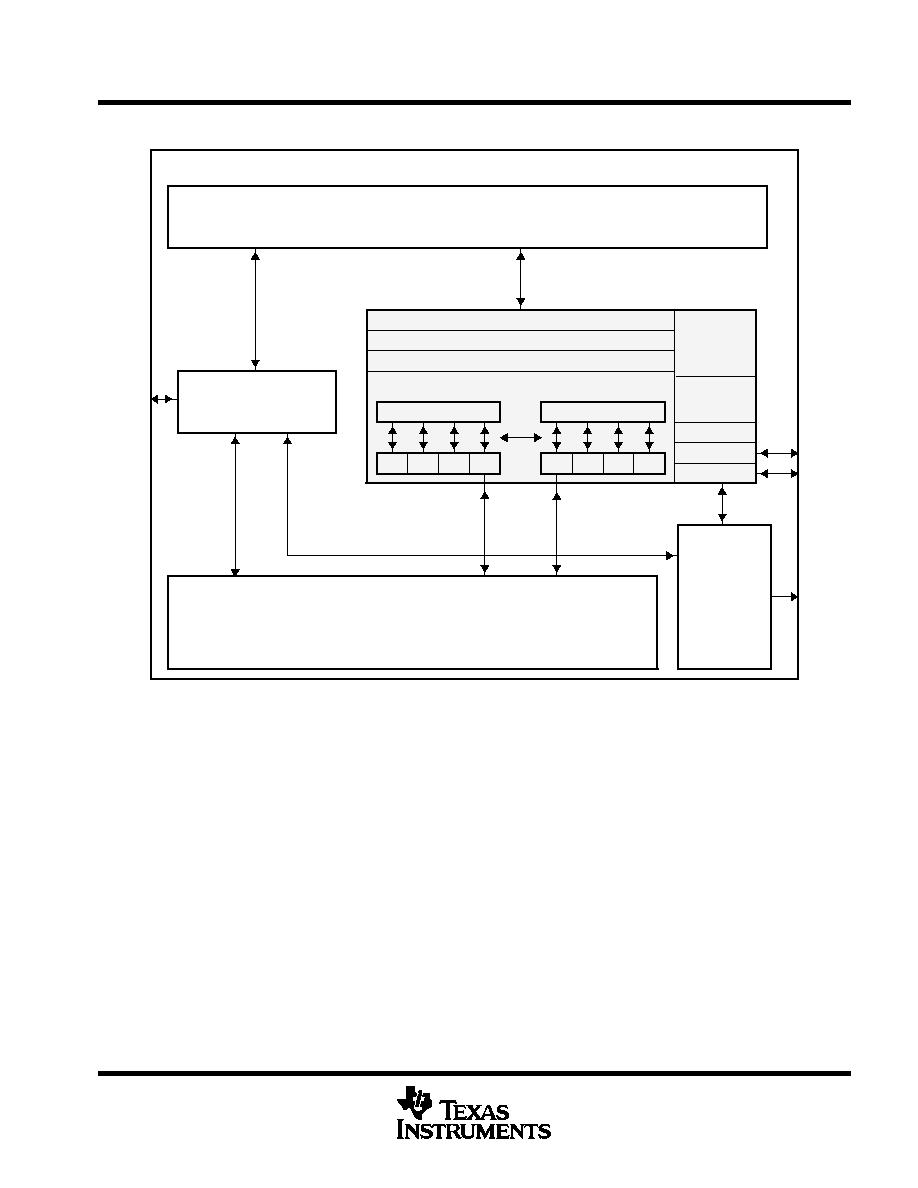
functional block diagram
EMIF
Timers
Interrupt Selector
McBSPs
HPI Control
DMA Control
EMIF Control
Host-Port Interface
PLL
Power
Down
Boot-
Config.
Peripheral
Bus
Controller
DMA
Controller
Data Memory
Data Memory
Controller
CPU
Program Memory Controller
Program Memory/Cache
SM320C6201B, SMJ320C6201B
DIGITAL SIGNAL PROCESSOR
SGUS031B APRIL 2000 REVISED AUGUST 2001
4
POST OFFICE BOX 1443
·
HOUSTON, TEXAS 772511443
CPU description
The CPU fetches VelociTI advanced very-long instruction words (VLIW) (256 bits wide) to supply up to eight
32-bit instructions to the eight functional units during every clock cycle. The VelociTI VLIW architecture features
controls by which all eight units do not have to be supplied with instructions if they are not ready to execute. The
first bit of every 32-bit instruction determines if the next instruction belongs to the same execute packet as the
previous instruction, or whether it should be executed in the following clock as a part of the next execute packet.
Fetch packets are always 256 bits wide; however, the execute packets can vary in size. The variable-length
execute packets are a key memory-saving feature, distinguishing the C62x CPU from other VLIW architectures.
The CPU features two sets of functional units. Each set contains four units and a register file. One set contains
functional units .L1, .S1, .M1, and .D1; the other set contains units .D2, .M2, .S2, and .L2. The two register files
each contain 16 32-bit registers for a total of 32 general-purpose registers. The two sets of functional units, along
with two register files, compose sides A and B of the CPU (see Figure 1 and Figure 2). The four functional units
on each side of the CPU can freely share the 16 registers belonging to that side. Additionally, each side features
a single data bus connected to all the registers on the other side, by which the two sets of functional units can
access data from the register files on the opposite side. While register access by functional units on the same
side of the CPU as the register file can service all the units in a single clock cycle, register access using the
register file across the CPU supports one read and one write per cycle.
Another key feature of the C62x CPU is the load/store architecture, where all instructions operate on registers
(as opposed to data in memory). Two sets of data-addressing units (.D1 and .D2) are responsible for all data
transfers between the register files and the memory. The data address driven by the .D units allows data
addresses generated from one register file to be used to load or store data to or from the other register file. The
C62x CPU supports a variety of indirect addressing modes using either linear- or circular-addressing modes
with 5- or 15-bit offsets. All instructions are conditional, and most can access any one of the 32 registers. Some
registers, however, are singled out to support specific addressing or to hold the condition for conditional
instructions (if the condition is not automatically "true"). The two .M functional units are dedicated for multiplies.
The two .S and .L functional units perform a general set of arithmetic, logical, and branch functions with results
available every clock cycle.
The processing flow begins when a 256-bit-wide instruction fetch packet is fetched from a program memory.
The 32-bit instructions destined for the individual functional units are "linked" together by "1" bits in the least
significant bit (LSB) position of the instructions. The instructions that are "chained" together for simultaneous
execution (up to eight in total) compose an execute packet. A "0" in the LSB of an instruction breaks the chain,
effectively placing the instructions that follow it in the next execute packet. If an execute packet crosses the fetch
packet boundary (256 bits wide), the assembler places it in the next fetch packet, while the remainder of the
current fetch packet is padded with NOP instructions. The number of execute packets within a fetch packet can
vary from one to eight. Execute packets are dispatched to their respective functional units at the rate of one per
clock cycle and the next 256-bit fetch packet is not fetched until all the execute packets from the current fetch
packet have been dispatched. After decoding, the instructions simultaneously drive all active functional units
for a maximum execution rate of eight instructions every clock cycle. While most results are stored in 32-bit
registers, they can be subsequently moved to memory as bytes or half-words as well. All load and store
instructions are byte-, half-word, or word-addressable.
SM320C6201B, SMJ320C6201B
DIGITAL SIGNAL PROCESSOR
SGUS031B APRIL 2000 REVISED AUGUST 2001
5
POST OFFICE BOX 1443
·
HOUSTON, TEXAS 772511443
CPU description (continued)
Á
Á
Á
Á
ÁÁ
Á
Á
Á
Á
ÁÁ
ÁÁ
Á
Á
Á
Á
ÁÁ
ÁÁ
Á
Á
ÁÁ
ÁÁ
C62x CPU
Á
Á
ÁÁ
ÁÁ
Á
Á
ÁÁ
ÁÁ
ÁÁ
ÁÁ
Á
Á
Á
Á
ÁÁ
ÁÁ
ÁÁ
ÁÁ
Á
Á
Á
Á
ÁÁ
ÁÁ
Á
Á
Á
Program Memory
32-Bit Address
256-Bit Data
External Memory
Interface
Data Memory
32-Bit Address
8-, 16-, 32-Bit Data
Program Fetch
Instruction Dispatch
Instruction Decode
Data Path A
Register File A
Data Path B
Register File B
.L1
.S1
.M1 .D1
.D2
.M2 .S2
.L2
Control
Registers
Control
Logic
Test
Emulation
Interrupts
Additional
Peripherals:
Timers,
Serial Ports,
etc.
Figure 1. 320C62x CPU Block Diagram