SN54LVTH374, SN74LVTH374 (Rev. H)
SN54LVTH374, SN74LVTH374
3.3 V ABT OCTAL EDGE TRIGGERED D TYPE FLIP FLOPS
WITH 3 STATE OUTPUTS
SCBS683H - MARCH 1997 - REVISED OCTOBER 2003
1
POST OFFICE BOX 655303
·
DALLAS, TEXAS 75265
D
Support Mixed-Mode Signal Operation
(5-V Input and Output Voltages With
3.3-V V
CC
)
D
Typical V
OLP
(Output Ground Bounce)
<0.8 V at V
CC
= 3.3 V, T
A
= 25
°
C
D
Support Unregulated Battery Operation
Down to 2.7 V
D
I
off
and Power-Up 3-State Support Hot
Insertion
D
Bus Hold on Data Inputs Eliminates the
Need for External Pullup/Pulldown
Resistors
D
Latch-Up Performance Exceeds 500 mA Per
JESD 17
D
ESD Protection Exceeds JESD 22
- 2000-V Human-Body Model (A114-A)
- 200-V Machine Model (A115-A)
description/ordering information
These octal flip-flops are designed specifically for
low-voltage (3.3-V) V
CC
operation, but with the
capability to provide a TTL interface to a
5-V system environment.
The eight flip-flops of the 'LVTH374 devices are
edge-triggered D-type flip-flops. On the positive
transition of the clock (CLK) input, the Q outputs
are set to the logic levels set up at the data (D)
inputs.
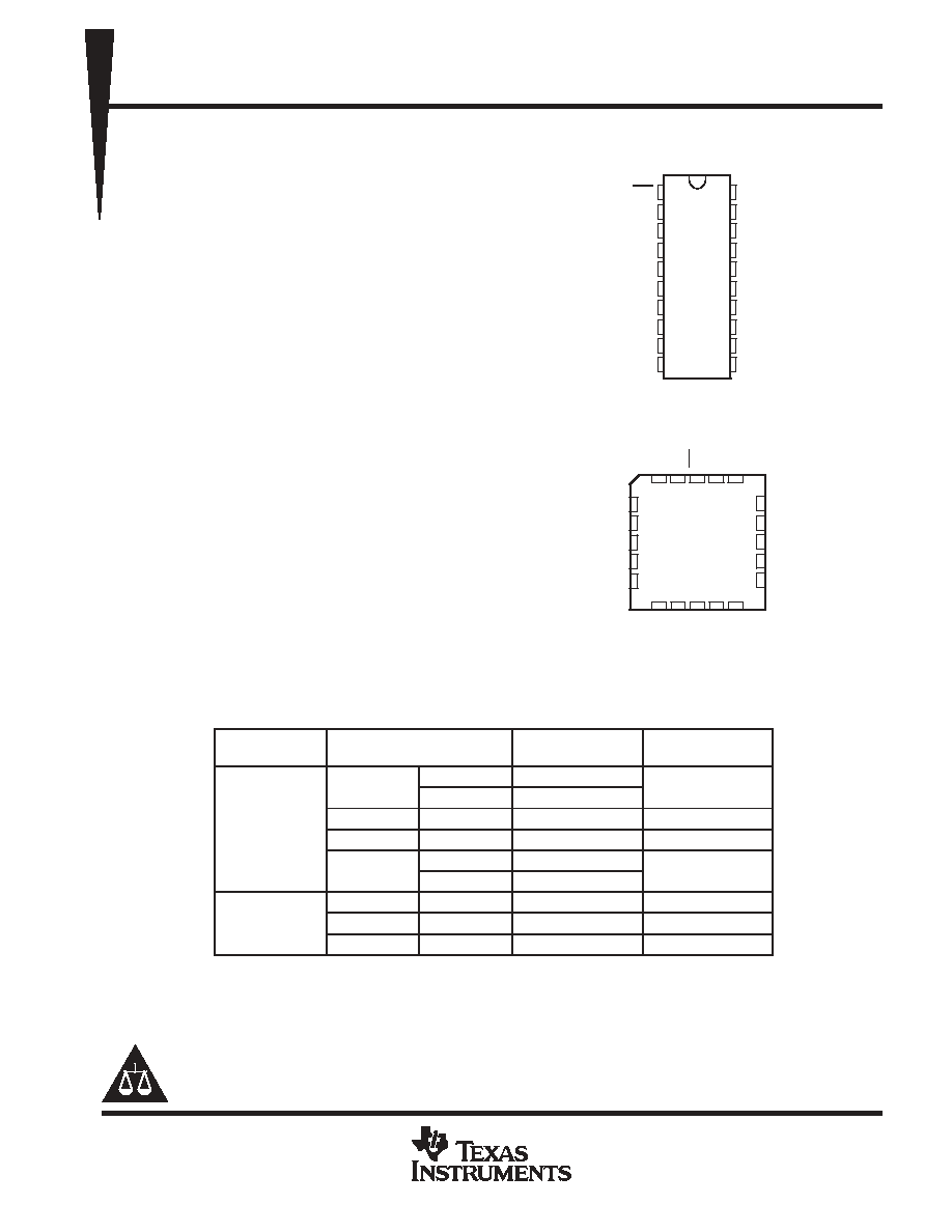
ORDERING INFORMATION
TA
PACKAGE
ORDERABLE
PART NUMBER
TOP-SIDE
MARKING
SOIC - DW
Tube
SN74LVTH374DW
LVTH374
SOIC - DW
Tape and reel
SN74LVTH374DWR
LVTH374
-40
°
C to 85
°
C
SOP - NS
Tape and reel
SN74LVTH374NSR
LVTH374
-40
°
C to 85
°
C
SSOP - DB
Tape and reel
SN74LVTH374DBR
LXH374
TSSOP - PW
Tube
SN74LVTH374PW
LXH374
TSSOP - PW
Tape and reel
SN74LVTH374PWR
LXH374
CDIP - J
Tube
SNJ54LVTH374J
SNJ54LVTH374J
-55
°
C to 125
°
C
CFP - W
Tube
SNJ54LVTH374W
SNJ54LVTH374W
-55 C to 125 C
LCCC - FK
Tube
SNJ54LVTH374FK
SNJ54LVTH374FK
Package drawings, standard packing quantities, thermal data, symbolization, and PCB design
guidelines are available at www.ti.com/sc/package.
Copyright
2003, Texas Instruments Incorporated
Please be aware that an important notice concerning availability, standard warranty, and use in critical applications of
Texas Instruments semiconductor products and disclaimers thereto appears at the end of this data sheet.
SN54LVTH374 . . . J OR W PACKAGE
SN74LVTH374 . . . DB, DW, NS, OR PW PACKAGE
(TOP VIEW)
SN54LVTH374 . . . FK PACKAGE
(TOP VIEW)
1
2
3
4
5
6
7
8
9
10
20
19
18
17
16
15
14
13
12
11
OE
1Q
1D
2D
2Q
3Q
3D
4D
4Q
GND
V
CC
8Q
8D
7D
7Q
6Q
6D
5D
5Q
CLK
3 2
1 20 19
9 10 11 12 13
4
5
6
7
8
18
17
16
15
14
2D
2Q
3Q
3D
4D
1D
1Q
OE
5Q
5D
8Q
4Q
GND
CLK
V
CC
8D
7D
7Q
6Q
6D
On products compliant to MIL PRF 38535, all parameters are tested
unless otherwise noted. On all other products, production
processing does not necessarily include testing of all parameters.
PRODUCTION DATA information is current as of publication date.
Products conform to specifications per the terms of Texas Instruments
standard warranty. Production processing does not necessarily include
testing of all parameters.
SN54LVTH374, SN74LVTH374
3.3 V ABT OCTAL EDGE TRIGGERED D TYPE FLIP FLOPS
WITH 3 STATE OUTPUTS
SCBS683H - MARCH 1997 - REVISED OCTOBER 2003
2
POST OFFICE BOX 655303
·
DALLAS, TEXAS 75265
description/ordering information (continued)
A buffered output-enable (OE) input can be used to place the eight outputs in either a normal logic state (high
or low logic levels) or the high-impedance state. In the high-impedance state, the outputs neither load nor drive
the bus lines significantly. The high-impedance state and increased drive provide the capability to drive bus
lines without need for interface or pullup components.
OE does not affect the internal operations of the flip-flops. Old data can be retained or new data can be entered
while the outputs are in the high-impedance state.
When V
CC
is between 0 and 1.5 V, the devices are in the high-impedance state during power up or power down.
However, to ensure the high-impedance state above 1.5 V, OE should be tied to V
CC
through a pullup resistor;
the minimum value of the resistor is determined by the current-sinking capability of the driver.
Active bus-hold circuitry holds unused or undriven inputs at a valid logic state. Use of pullup or pulldown resistors
with the bus-hold circuitry is not recommended.
These devices are fully specified for hot-insertion applications using I
off
and power-up 3-state. The I
off
circuitry
disables the outputs, preventing damaging current backflow through the devices when they are powered down.
The power-up 3-state circuitry places the outputs in the high-impedance state during power up and power down,
which prevents driver conflict.
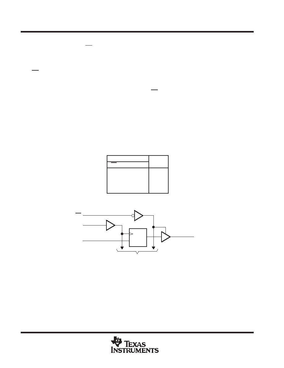
FUNCTION TABLE
(each flip-flop)
INPUTS
OUTPUT
OE
CLK
D
OUTPUT
Q
L
H
H
L
L
L
L
H or L
X
Q0
H
X
X
Z
logic diagram (positive logic)
OE
To Seven Other Channels
1
11
3
2
CLK
1D
C1
1D
1Q
SN54LVTH374, SN74LVTH374
3.3 V ABT OCTAL EDGE TRIGGERED D TYPE FLIP FLOPS
WITH 3 STATE OUTPUTS
SCBS683H - MARCH 1997 - REVISED OCTOBER 2003
3
POST OFFICE BOX 655303
·
DALLAS, TEXAS 75265
absolute maximum ratings over operating free-air temperature range (unless otherwise noted)
Supply voltage range, V
CC
-0.5 V to 4.6 V
. . . . . . . . . . . . . . . . . . . . . . . . . . . . . . . . . . . . . . . . . . . . . . . . . . . . . . . . .
Input voltage range, V
I
(see Note 1)
-0.5 V to 7 V
. . . . . . . . . . . . . . . . . . . . . . . . . . . . . . . . . . . . . . . . . . . . . . . . . .
Voltage range applied to any output in the high-impedance
or power-off state, V
O
(see Note 1)
-0.5 V to 7 V
. . . . . . . . . . . . . . . . . . . . . . . . . . . . . . . . . . . . . . . . . . . . . . . .
Voltage range applied to any output in the high state, V
O
(see Note 1)
-0.5 V to V
CC
+ 0.5 V
. . . . . . . . . . . . .
Current into any output in the low state, I
O
: SN54LVTH374 96
mA
. . . . . . . . . . . . . . . . . . . . . . . . . . . . . . . . . . .
SN74LVTH374 128
mA
. . . . . . . . . . . . . . . . . . . . . . . . . . . . . . . . . .
Current into any output in the high state, I
O
(see Note 2): SN54LVTH374
48 mA
. . . . . . . . . . . . . . . . . . . . . . .
SN74LVTH374 64
mA
. . . . . . . . . . . . . . . . . . . . . . .
Input clamp current, I
IK
(V
I
< 0)
-50 mA
. . . . . . . . . . . . . . . . . . . . . . . . . . . . . . . . . . . . . . . . . . . . . . . . . . . . . . . . . . .
Output clamp current, I
OK
(V
O
< 0)
-50 mA
. . . . . . . . . . . . . . . . . . . . . . . . . . . . . . . . . . . . . . . . . . . . . . . . . . . . . . . .
Package thermal impedance,
JA
(see Note 3): DB package
70
°
C/W
. . . . . . . . . . . . . . . . . . . . . . . . . . . . . . . . .
DW package
58
°
C/W
. . . . . . . . . . . . . . . . . . . . . . . . . . . . . . . . .
NS package
60
°
C/W
. . . . . . . . . . . . . . . . . . . . . . . . . . . . . . . . .
PW package
83
°
C/W
. . . . . . . . . . . . . . . . . . . . . . . . . . . . . . . . .
Storage temperature range, T
stg
-65
°
C to 150
°
C
. . . . . . . . . . . . . . . . . . . . . . . . . . . . . . . . . . . . . . . . . . . . . . . . . . .
Stresses beyond those listed under "absolute maximum ratings" may cause permanent damage to the device. These are stress ratings only, and
functional operation of the device at these or any other conditions beyond those indicated under "recommended operating conditions" is not
implied. Exposure to absolute-maximum-rated conditions for extended periods may affect device reliability.
NOTES:
1. The input and output negative-voltage ratings may be exceeded if the input and output clamp-current ratings are observed.
2. This current flows only when the output is in the high state and VO > VCC.
3. The package thermal impedance is calculated in accordance with JESD 51-7.
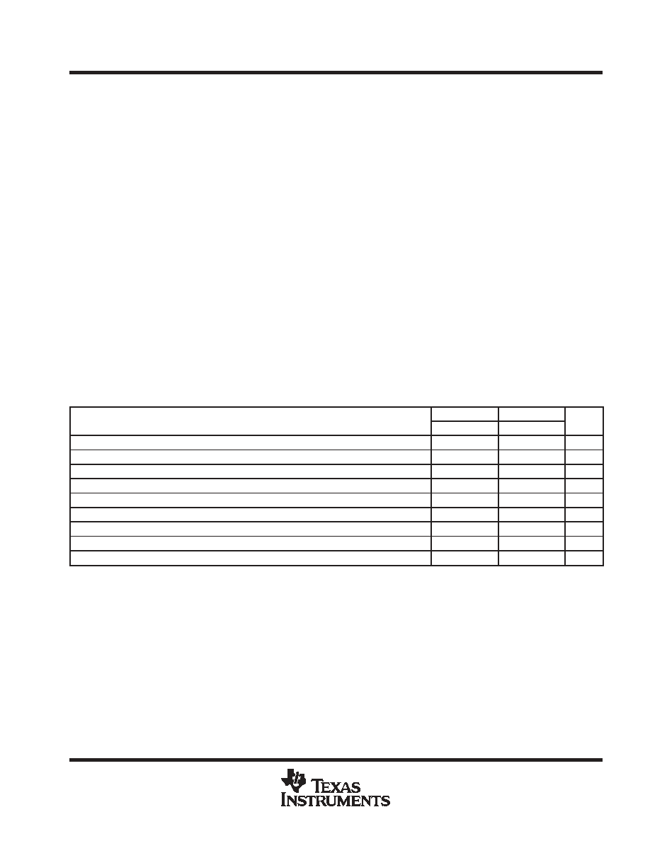
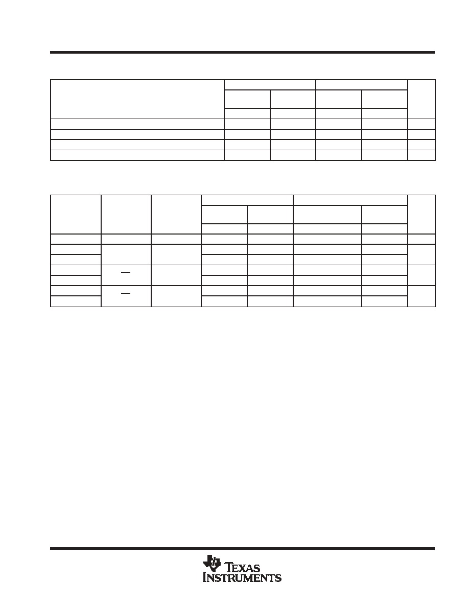
recommended operating conditions (see Note 4)
SN54LVTH374
SN74LVTH374
UNIT
MIN
MAX
MIN
MAX
UNIT
VCC
Supply voltage
2.7
3.6
2.7
3.6
V
VIH
High-level input voltage
2
2
V
VIL
Low-level input voltage
0.8
0.8
V
VI
Input voltage
5.5
5.5
V
IOH
High-level output current
-24
-32
mA
IOL
Low-level output current
48
64
mA
t/
v
Input transition rise or fall rate
10
10
ns/V
t/
VCC
Power-up ramp rate
200
200
µ
s/V
TA
Operating free-air temperature
-55
125
-40
85
°
C
NOTE 4: All unused control inputs of the device must be held at VCC or GND to ensure proper device operation. Refer to the TI application report,
Implications of Slow or Floating CMOS Inputs, literature number SCBA004.
SN54LVTH374, SN74LVTH374
3.3 V ABT OCTAL EDGE TRIGGERED D TYPE FLIP FLOPS
WITH 3 STATE OUTPUTS
SCBS683H - MARCH 1997 - REVISED OCTOBER 2003
4
POST OFFICE BOX 655303
·
DALLAS, TEXAS 75265
electrical characteristics over recommended operating free-air temperature range (unless
otherwise noted)
PARAMETER
TEST CONDITIONS
SN54LVTH374
SN74LVTH374
UNIT
PARAMETER
TEST CONDITIONS
MIN
TYP
MAX
MIN
TYP
MAX
UNIT
VIK
VCC = 2.7 V,
II = -18 mA
-1.2
-1.2
V
VCC = 2.7 V to 3.6 V,
IOH = -100
µ
A
VCC-0.2
VCC-0.2
VOH
VCC = 2.7 V,
IOH = -8 mA
2.4
2.4
V
VOH
VCC = 3 V
IOH = -24 mA
2
V
VCC = 3 V
IOH = -32 mA
2
VCC = 2.7 V
IOL = 100
µ
A
0.2
0.2
VCC = 2.7 V
IOL = 24 mA
0.5
0.5
VOL
IOL = 16 mA
0.4
0.4
V
VOL
VCC = 3 V
IOL = 32 mA
0.5
0.5
V
VCC = 3 V
IOL = 48 mA
0.55
IOL = 64 mA
0.55
VCC = 0 or 3.6 V,
VI = 5.5 V
10
10
II
Control
inputs
VCC = 3.6 V,
VI = VCC or GND
±
1
±
1
µ
A
II
Data
VCC = 3.6 V
VI = VCC
1
1
µ
A
Data
inputs
VCC = 3.6 V
VI = 0
-5
-5
Ioff
VCC = 0,
VI or VO = 0 to 4.5 V
±
100
µ
A
VCC = 3 V
VI = 0.8 V
75
75
II(hold)
Data
inputs
VCC = 3 V
VI = 2 V
-75
-75
µ
A
II(hold)
Data
inputs
VCC = 3.6 V,
VI = 0 to 3.6 V
500
-750
µ
A
IOZH
VCC = 3.6 V,
VO = 3 V
5
5
µ
A
IOZL
VCC = 3.6 V,
VO = 0.5 V
-5
-5
µ
A
IOZPU
VCC = 0 to 1.5 V, VO = 0.5 V to 3 V,
OE = don't care
±
100
±
100
µ
A
IOZPD
VCC = 1.5 V to 0, VO = 0.5 V to 3 V,
OE = don't care
±
100
±
100
µ
A
VCC = 3.6 V,
Outputs high
0.19
0.19
ICC
VCC = 3.6 V,
IO = 0,
V = V
or GND
Outputs low
5
5
mA
ICC
IO = 0,
VI = VCC or GND
Outputs disabled
0.19
0.19
mA
ICC§
VCC = 3 V to 3.6 V, One input at VCC - 0.6 V,
Other inputs at VCC or GND
0.2
0.2
mA
Ci
VI = 3 V or 0
3
3
pF
Co
VO = 3 V or 0
7
7
pF
On products compliant to MIL-PRF-38535, this parameter is not production tested.
All typical values are at VCC = 3.3 V, TA = 25
°
C.
This is the bus-hold maximum dynamic current. It is the minimum overdrive current required to switch the input from one state to another.
§ This is the increase in supply current for each input that is at the specified TTL voltage level, rather than VCC or GND.
SN54LVTH374, SN74LVTH374
3.3 V ABT OCTAL EDGE TRIGGERED D TYPE FLIP FLOPS
WITH 3 STATE OUTPUTS
SCBS683H - MARCH 1997 - REVISED OCTOBER 2003
5
POST OFFICE BOX 655303
·
DALLAS, TEXAS 75265
timing requirements over recommended operating free-air temperature range (unless otherwise
noted) (see Figure 1)
SN54LVTH374
SN74LVTH374
VCC = 3.3 V
±
0.3 V
VCC = 2.7 V
VCC = 3.3 V
±
0.3 V
VCC = 2.7 V
UNIT
MIN
MAX
MIN
MAX
MIN
MAX
MIN
MAX
fclock
Clock frequency
150
150
150
150
MHz
tw
Pulse duration, CLK high or low
3.3
3.3
3.3
3.3
ns
tsu
Setup time, data before CLK
1.6
2
1.5
2
ns
th
Hold time, data after CLK
0.8
0.5
0.8
0
ns
switching characteristics over recommended ranges of supply voltage and operating free-air
temperature, C
L
= 50 pF (unless otherwise noted) (see Figure 1)
SN54LVTH374
SN74LVTH374
PARAMETER
FROM
(INPUT)
TO
(OUTPUT)
VCC = 3.3 V
±
0.3 V
VCC = 2.7 V
VCC = 3.3 V
±
0.3 V
VCC = 2.7 V
UNIT
(INPUT)
(OUTPUT)
MIN
MAX
MIN
MAX
MIN
TYP
MAX
MIN
MAX
fmax
150
150
150
150
MHz
tPLH
CLK
Q
1
5.1
5.6
1.8
2.9
4.5
5
ns
tPHL
CLK
Q
1.5
5.1
5.2
1.8
2.9
4.2
4.3
ns
tPZH
OE
Q
0.8
5.6
6.6
1.3
2.8
4.7
5.6
ns
tPZL
OE
Q
1.2
5.4
6.2
1.6
3
4.7
5.2
ns
tPHZ
OE
Q
1.5
5.6
5.7
1.9
3
4.6
4.9
ns
tPLZ
OE
Q
0.8
5.2
5.3
2
3.1
4.5
4.6
ns
All typical values are at VCC = 3.3 V, TA = 25
°
C.