
THS4051, THS4052
70-MHz HIGH-SPEED AMPLIFIERS
SLOS238C≠ MAY 1999 ≠ REVISED MAY 2000
1
POST OFFICE BOX 655303
∑
DALLAS, TEXAS 75265
D
High Speed
≠ 70 MHz Bandwidth (G = 1, ≠3 dB)
≠ 240 V/
µ
s Slew Rate
≠ 60-ns Settling Time (0.1%)
D
High Output Drive, I
O
= 100 mA (typ)
D
Excellent Video Performance
≠ 0.1 dB Bandwidth of 30 MHz (G = 1)
≠ 0.01% Differential Gain
≠ 0.01
∞
Differential Phase
D
Very Low Distortion
≠ THD = ≠82 dBc (f = 1 MHz, R
L
= 150
)
≠ THD = ≠89 dBc (f = 1 MHz, R
L
= 1 k
)
D
Wide Range of Power Supplies
≠ V
CC
=
±
5 V to
±
15 V
D
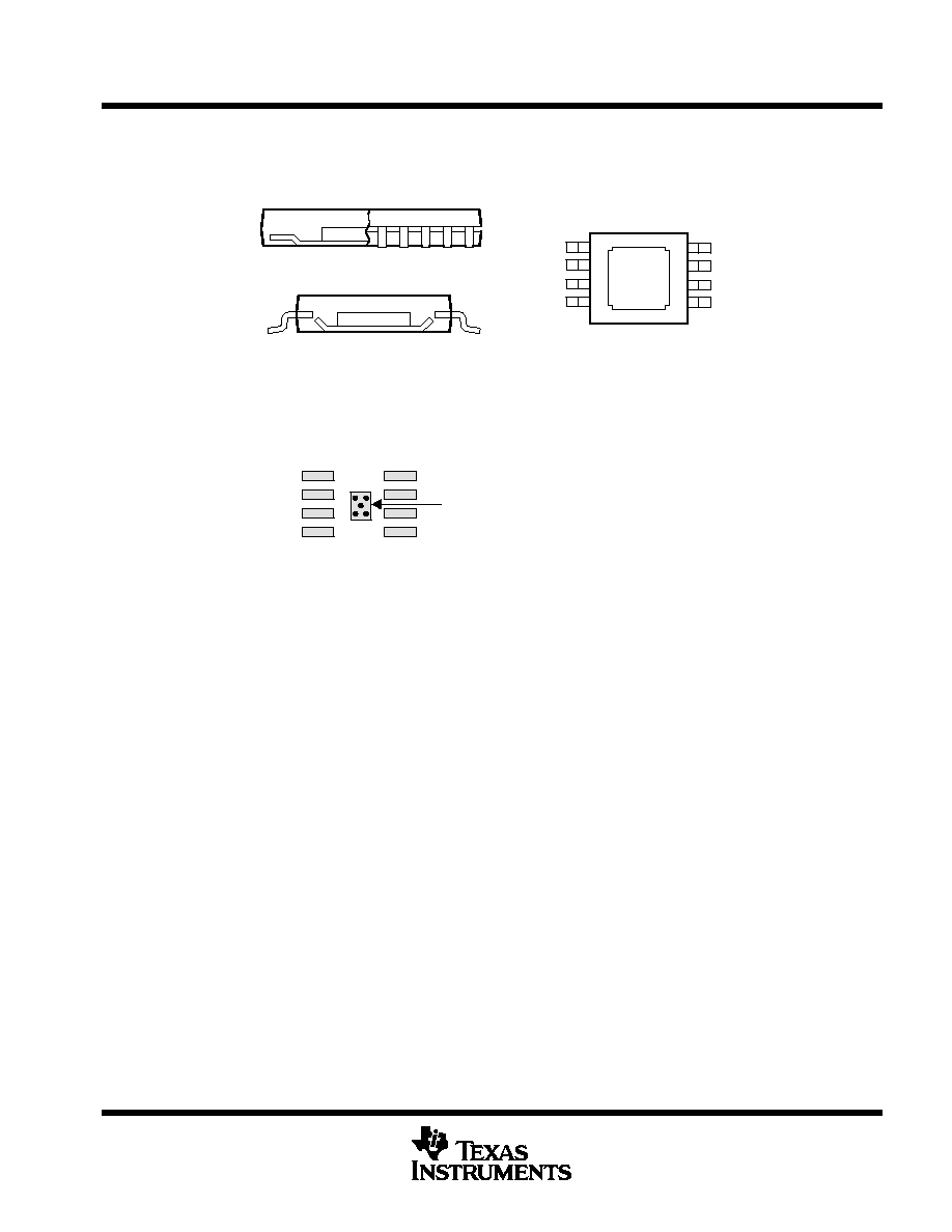
Available in Standard SOIC, MSOP
PowerPAD
TM
, JG or FK Package
D
Evaluation Module Available
description
The THS4051 and THS4052 are general-pur-
pose, single/dual, high-speed voltage feedback
amplifiers ideal for a wide range of applications
including video, communication, and imaging.
The devices offer very good ac performance with
70-MHz bandwidth, 240-V/
µ
s slew rate, and
60-ns settling time (0.1%). The THS4051/2 are
stable at all gains for both inverting and non-
inverting configurations. These amplifiers have a
high output drive capability of 100 mA and draw
only 8.5-mA supply current per channel. Excellent
professional video results can be obtained with
the low differential gain/phase errors of 0.01%/
0.01
∞
and wide 0.1 dB flatness to 30 MHz. For
applications requiring low distortion, the
THS4051/2 is ideally suited with total harmonic
distortion of ≠82 dBc at 1 MHz.
RELATED DEVICES
DEVICE
DESCRIPTION
THS4011/2
THS4031/2
THS4081/2
290-MHz Low Distortion High-Speed Amplifiers
100-MHz Low Noise High-Speed Amplifiers
175-MHz Low Power High-Speed Amplifiers
PowerPAD is a trademark of Texas Instruments.
Copyright
©
2000, Texas Instruments Incorporated
PRODUCTION DATA information is current as of publication date.
Products conform to specifications per the terms of Texas Instruments
standard warranty. Production processing does not necessarily include
testing of all parameters.
Please be aware that an important notice concerning availability, standard warranty, and use in critical applications of
Texas Instruments semiconductor products and disclaimers thereto appears at the end of this data sheet.
THS4052
D AND DGN PACKAGE
(TOP VIEW)
1
2
3
4
8
7
6
5
1OUT
1IN ≠
1IN +
≠V
CC
V
CC+
2OUT
2IN≠
2IN+
1
2
3
4
8
7
6
5
NULL
IN ≠
IN +
V
CC≠
NULL
V
CC+
OUT
NC
THS4051
D, DGN, AND JG PACKAGE
(TOP VIEW)
NC ≠ No internal connection
Cross Section View Showing
PowerPAD
TM
Option (DGN)
This device is in the Product Preview stage of development.
Please contact your local TI sales office for availability.
19
20
1
3
2
17
18
16
15
14
13
12
11
9
10
5
4
6
7
8
NC
V
CC+
NC
OUT
NC
NC
IN≠
NC
IN+
NC
NC
NULL
NC
NULL
NC
V
NC
NC
NC
NC
THS4051
FK PACKAGE
(TOP VIEW)
CC≠
CAUTION: The THS4051 and THS4052 provide ESD protection circuitry. However, permanent damage can still occur if this device
is subjected to high-energy electrostatic discharges. Proper ESD precautions are recommended to avoid any performance
degradation or loss of functionality.
On products compliant to MIL-PRF-38535, all parameters are tested
unless otherwise noted. On all other products, production
processing does not necessarily include testing of all parameters.

THS4051, THS4052
70-MHz HIGH-SPEED AMPLIFIERS
SLOS238C≠ MAY 1999 ≠ REVISED MAY 2000
2
POST OFFICE BOX 655303
∑
DALLAS, TEXAS 75265
≠100
≠90
≠80
≠70
≠60
≠50
≠40
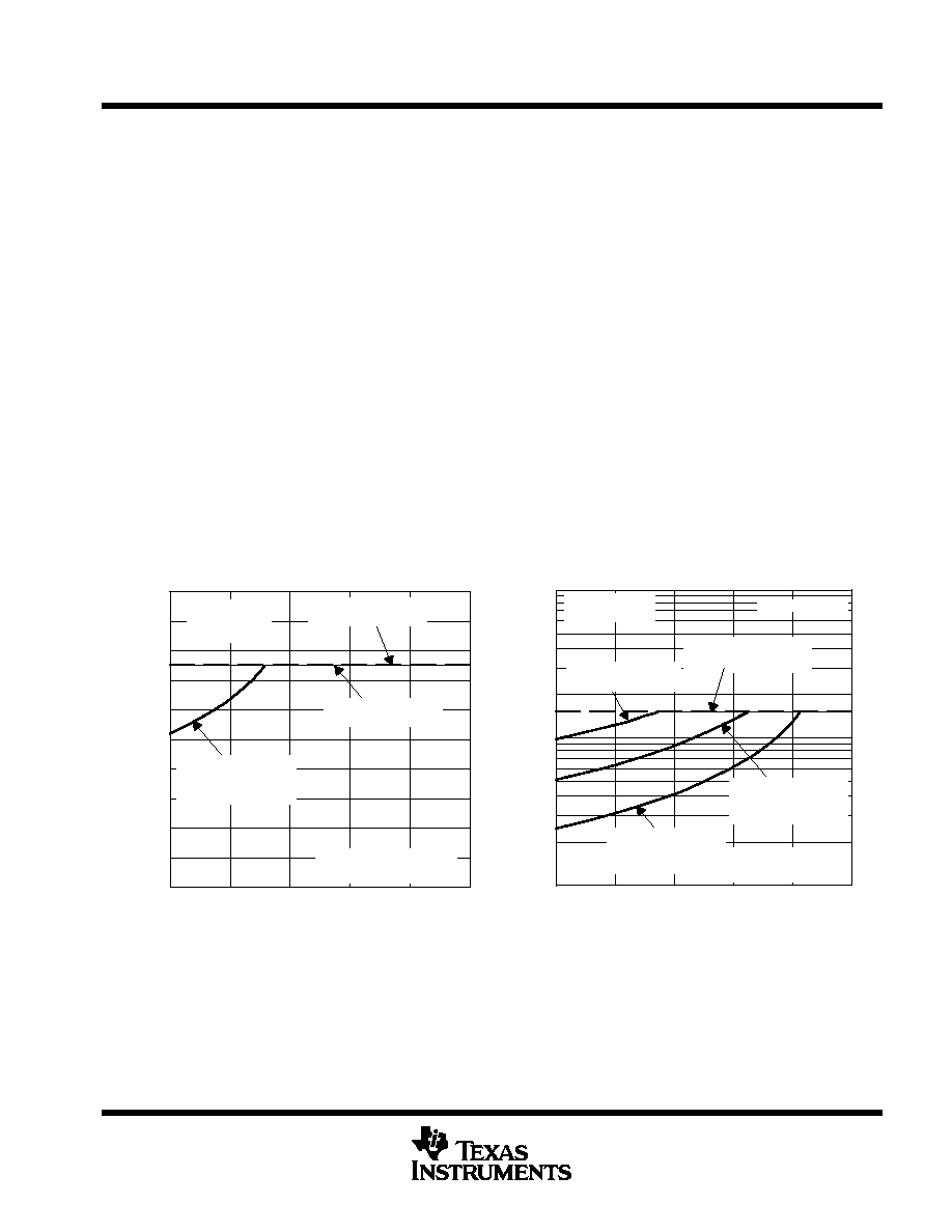
TOTAL HARMONIC DISTORTION
vs
FREQUENCY
f - Frequency - Hz
20M
10M
100k
1M
THD - T
otal Harmonic Distortion - dBc
RL = 150
RL = 1 k
VCC =
±
15 V
Gain = 2
VO(PP) = 2 V
AVAILABLE OPTIONS
PACKAGED DEVICES
TA
NUMBER
OF
CHANNELS
PLASTIC
SMALL
OUTLINE
PLASTIC MSOP
(DGN)
CERAMIC DIP
(JG)
CHIP
CARRIER
EVALUATION
MODULE
CHANNELS
OUTLINE
(D)
DEVICE
SYMBOL
(JG)
CARRIER
(FK)
0
∞
C to 70
∞
C
1
THS4051CD
THS4051CDGN
ACQ
--
--
THS4051EVM
0
∞
C to 70
∞
C
2
THS4052CD
THS4052CDGN
ACE
--
--
THS4052EVM
≠ 40
∞
C to 85
∞
C
1
THS4051ID
THS4051IDGN
ACR
--
--
--
≠ 40
∞
C to 85
∞
C
2
THS4052ID
THS4052IDGN
ACF
--
--
--
≠ 55
∞
C to 125
∞
C
1
--
--
--
THS4051MJG
THS4051MFK
--
The D and DGN packages are available taped and reeled. Add an R suffix to the device type (i.e., THS4051CDGN).
This device is in the Product Preview stage of development. Please contact your local TI sales office for availability.
functional block diagram
OUT
8
6
1
IN≠
IN+
2
3
Null
Figure 1. THS4051 ≠ Single Channel
1OUT
1IN≠
1IN+
VCC
2OUT
2IN≠
2IN+
≠VCC
Figure 2. THS4052 ≠ Dual Channel

THS4051, THS4052
70-MHz HIGH-SPEED AMPLIFIERS
SLOS238C≠ MAY 1999 ≠ REVISED MAY 2000
3
POST OFFICE BOX 655303
∑
DALLAS, TEXAS 75265
absolute maximum ratings over operating free-air temperature (unless otherwise noted)
Supply voltage, V
CC
±
16.5 V
. . . . . . . . . . . . . . . . . . . . . . . . . . . . . . . . . . . . . . . . . . . . . . . . . . . . . . . . . . . . . . . . . . . .
Input voltage, V
I
±
V
CC
. . . . . . . . . . . . . . . . . . . . . . . . . . . . . . . . . . . . . . . . . . . . . . . . . . . . . . . . . . . . . . . . . . . . . . . . . .
Output current, I
O
150 mA
. . . . . . . . . . . . . . . . . . . . . . . . . . . . . . . . . . . . . . . . . . . . . . . . . . . . . . . . . . . . . . . . . . . . . . .
Differential input voltage, V
IO
±
4 V
. . . . . . . . . . . . . . . . . . . . . . . . . . . . . . . . . . . . . . . . . . . . . . . . . . . . . . . . . . . . . . . .
Continuous total power dissipation
See Dissipation Rating Table
. . . . . . . . . . . . . . . . . . . . . . . . . . . . . . . . . . . . .
Maximum junction temperature, T
J
150
∞
C
. . . . . . . . . . . . . . . . . . . . . . . . . . . . . . . . . . . . . . . . . . . . . . . . . . . . . . . .
Operating free-air temperature, T
A
:
C-suffix 0
∞
C to 70
∞
C
. . . . . . . . . . . . . . . . . . . . . . . . . . . . . . . . . . . . . . . . . . .
I-suffix ≠ 40
∞
C to 85
∞
C
. . . . . . . . . . . . . . . . . . . . . . . . . . . . . . . . . . . . . . . . . .
M-suffix ≠55
∞
C to 125
∞
C
. . . . . . . . . . . . . . . . . . . . . . . . . . . . . . . . . . . . . . . .
Storage temperature, T
stg
≠ 65
∞
C to 150
∞
C
. . . . . . . . . . . . . . . . . . . . . . . . . . . . . . . . . . . . . . . . . . . . . . . . . . . . . . . . .
Lead temperature 1,6 mm (1/16 inch) from case for 10 seconds
300
∞
C
. . . . . . . . . . . . . . . . . . . . . . . . . . . . . . .
Lead temperature 1,6 mm (1/16 inch) from case for 60 seconds, JG package
300
∞
C
. . . . . . . . . . . . . . . . . . . .
Case temperature for 60 seconds, FK package
260
∞
C
. . . . . . . . . . . . . . . . . . . . . . . . . . . . . . . . . . . . . . . . . . . . . .
Stresses beyond those listed under "absolute maximum ratings" may cause permanent damage to the device. These are stress ratings only and
functional operation of the device at these or any other conditions beyond those indicated under "recommended operating conditions" is not
implied. Exposure to absolute-maximum-rated conditions for extended periods may affect device reliability.
DISSIPATION RATING TABLE
PACKAGE
JA
JC
TA = 25
∞
C
PACKAGE
JA
(
∞
C/W)
JC
(
∞
C/W)
A
POWER RATING
D
167
38.3
740 mW
DGNß
58.4
4.7
2.14 W
JG
119
28
1050 mW
FK
87.7
20
1375 mW
This data was taken using the JEDEC standard Low-K test PCB. For the JEDEC Proposed High-K
test PCB, the
JA is 95
∞
C/W with a power rating at TA = 25
∞
C of 1.32 W.
ß This data was taken using 2 oz. trace and copper pad that is soldered directly to a 3 in.
◊
3 in. PC.
For further information, refer to
Application Information section of this data sheet.
recommended operating conditions
MIN
NOM
MAX
UNIT
Supply voltage VCC and VCC
Dual supply
±
4.5
±
16
V
Supply voltage, VCC+ and VCC≠
Single supply
9
32
V
C-suffix
0
70
Operating free-air temperature, TA
I-suffix
≠40
85
∞
C
M-suffix
≠55
125
THS4051, THS4052
70-MHz HIGH-SPEED AMPLIFIERS
SLOS238C≠ MAY 1999 ≠ REVISED MAY 2000
4
POST OFFICE BOX 655303
∑
DALLAS, TEXAS 75265
electrical characteristics at T
A
= 25
∞
C, V
CC
=
±
15 V, R
L
= 150
(unless otherwise noted)
dynamic performance
PARAMETER
TEST CONDITIONS
THS405xC, THS405xI
UNIT
PARAMETER
TEST CONDITIONS
MIN
TYP
MAX
UNIT
VCC =
±
15 V
Gain = 1
70
MHz
Dynamic performance small-signal bandwidth
VCC =
±
5 V
Gain = 1
70
MHz
y
g
(≠3 dB)
VCC =
±
15 V
Gain = 2
38
MHz
BW
VCC =
±
5 V
Gain = 2
38
MHz
BW
Bandwidth for 0 1 dB flatness
VCC =
±
15 V
Gain = 1
30
MHz
Bandwidth for 0.1 dB flatness
VCC =
±
5 V
Gain = 1
30
MHz
Full power bandwidthß
VO(pp) = 20 V,
VCC =
±
15 V
3.8
MHz
Full power bandwidthß
VO(pp) = 5 V,
VCC =
±
5 V
12.7
MHz
SR
Slew rate
VCC =
±
15 V,
20-V step,
Gain = 5
240
V/
µ
s
SR
Slew rate
VCC =
±
5 V,
5-V step
Gain = ≠1
200
V/
µ
s
Settling time to 0 1%
VCC =
±
15 V,
5-V step
Gain = 1
60
ns
t
Settling time to 0.1%
VCC =
±
5 V,
2-V step
Gain = ≠1
60
ns
ts
Settling time to 0 01%
VCC =
±
15 V,
5-V step
Gain = 1
130
ns
Settling time to 0.01%
VCC =
±
5 V,
2-V step
Gain = ≠1
140
ns
Full range = 0
∞
C to 70
∞
C for C suffix and ≠ 40
∞
C to 85
∞
C for I suffix
Slew rate is measured from an output level range of 25% to 75%.
ß Full power bandwidth = slew rate/2
VO(Peak).
noise/distortion performance
PARAMETER
TEST CONDITIONS
THS405xC, THS405xI
UNIT
PARAMETER
TEST CONDITIONS
MIN
TYP
MAX
UNIT
VCC =
±
15 V
RL = 150
≠82
THD
Total harmonic distortion
VO(pp) = 2 V,
VCC =
±
15 V
RL = 1 k
≠89
dBc
THD
Total harmonic distortion
O(
)
,
f = 1 MHz, Gain = 2
VCC =
±
5 V
RL = 150
≠78
dBc
VCC =
±
5 V
RL = 1 k
≠87
Vn
Input voltage noise
VCC =
±
5 V or
±
15 V,
f = 10 kHz
14
nV/
Hz
In
Input current noise
VCC =
±
5 V or
±
15 V,
f = 10 kHz
0.9
pA/
Hz
Differential gain error
Gain = 2,
NTSC,
VCC =
±
15 V
0.01%
Differential gain error
,
40 IRE modulation,
,
±
100 IRE ramp
VCC =
±
5 V
0.01%
Differential phase error
Gain = 2,
NTSC,
VCC =
±
15 V
0.01
∞
Differential phase error
,
40 IRE modulation,
,
±
100 IRE ramp
VCC =
±
5 V
0.03
∞
Channel-to-channel crosstalk
(THS4052 only)
VCC =
±
5 V or
±
15 V,
f = 1 MHz
≠57
dB
Full range = 0
∞
C to 70
∞
C for C suffix and ≠ 40
∞
C to 85
∞
C for I suffix.

THS4051, THS4052
70-MHz HIGH-SPEED AMPLIFIERS
SLOS238C≠ MAY 1999 ≠ REVISED MAY 2000
5
POST OFFICE BOX 655303
∑
DALLAS, TEXAS 75265
electrical characteristics at T
A
= 25
∞
C, V
CC
=
±
15 V, R
L
= 150
(unless otherwise noted) (continued)
dc performance
PARAMETER
TEST CONDITIONS
THS405xC, THS405xI
UNIT
PARAMETER
TEST CONDITIONS
MIN
TYP
MAX
UNIT
VCC =
±
15 V RL = 1 k
VO =
±
10 V
TA = 25
∞
C
5
9
V/mV
Open loop gain
VCC =
±
15 V, RL = 1 k
VO =
±
10 V
TA = full range
3
V/mV
Open loop gain
VCC =
±
5 V RL = 250
VO =
±
2 5 V
TA = 25
∞
C
2.5
6
V/mV
VCC =
±
5 V, RL = 250
VO =
±
2.5 V
TA = full range
2
V/mV
VOS
Input offset voltage
VCC =
±
5 V or
±
15 V
TA = 25
∞
C
2.5
10
mV
VOS
Input offset voltage
VCC =
±
5 V or
±
15 V
TA = full range
12
mV
Offset voltage drift
VCC =
±
5 V or
±
15 V
TA = full range
15
µ
V/
∞
C
IIB
Input bias current
VCC =
±
5 V or
±
15 V
TA = 25
∞
C
2.5
6
µ
A
IIB
Input bias current
VCC =
±
5 V or
±
15 V
TA = full range
8
µ
A
IOS
Input offset current
VCC =
±
5 V or
±
15 V
TA = 25
∞
C
35
250
nA
IOS
Input offset current
VCC =
±
5 V or
±
15 V
TA = full range
400
nA
Offset current drift
TA = full range
0.3
nA/
∞
C
Full range = 0
∞
C to 70
∞
C for C suffix and ≠ 40
∞
C to 85
∞
C for I suffix
input characteristics
PARAMETER
TEST CONDITIONS
THS405xC, THS405xI
UNIT
PARAMETER
TEST CONDITIONS
MIN
TYP
MAX
UNIT
VICR
Common mode input voltage range
VCC =
±
15 V
±
13.8
±
14.3
V
VICR
Common-mode input voltage range
VCC =
±
5 V
±
3.8
±
4.3
V
CMRR
Common mode rejection ratio
VCC =
±
15 V,
VICR =
±
12 V
TA = full range
70
100
dB
CMRR
Common mode rejection ratio
VCC =
±
5 V,
VICR =
±
2.5 V
TA = full range
70
100
dB
ri
Input resistance
1
M
Ci
Input capacitance
1.5
pF
Full range = 0
∞
C to 70
∞
C for C suffix and ≠ 40
∞
C to 85
∞
C for I suffix
output characteristics
PARAMETER
TEST CONDITIONS
THS405xC, THS405xI
UNIT
PARAMETER
TEST CONDITIONS
MIN
TYP
MAX
UNIT
VCC =
±
15 V
RL = 250
±
11.5
±
13
V
VO
Output voltage swing
VCC =
±
5 V
RL = 150
±
3.2
±
3.5
V
VO
Output voltage swing
VCC =
±
15 V
RL = 1 k
±
13
±
13.6
V
VCC =
±
5 V
RL = 1 k
±
3.5
±
3.8
V
IO
Output current
VCC =
±
15 V
RL = 20
80
100
mA
IO
Output current
VCC =
±
5 V
RL = 20
50
75
mA
ISC
Short-circuit current
VCC =
±
15 V
150
mA
RO
Output resistance
Open loop
13
Full range = 0
∞
C to 70
∞
C for C suffix and ≠ 40
∞
C to 85
∞
C for I suffix
Observe power dissipation ratings to keep the junction temperature below the absolute maximum rating when the output is heavily loaded or
shorted. See the absolute maximum ratings section of this data sheet for more information.

THS4051, THS4052
70-MHz HIGH-SPEED AMPLIFIERS
SLOS238C≠ MAY 1999 ≠ REVISED MAY 2000
6
POST OFFICE BOX 655303
∑
DALLAS, TEXAS 75265
electrical characteristics at T
A
= 25
∞
C, V
CC
=
±
15 V, R
L
= 150
(unless otherwise noted) (continued)
power supply
PARAMETER
TEST CONDITIONS
THS405xC, THS405xI
UNIT
PARAMETER
TEST CONDITIONS
MIN
TYP
MAX
UNIT
VCC
Supply voltage operating range
Dual supply
±
4.5
±
16.5
V
VCC
Supply voltage operating range
Single supply
9
33
V
VCC =
±
15 V
TA = 25
∞
C
8.5
10.5
ICC
Supply current (per amplifier)
VCC =
±
15 V
TA = full range
11.5
mA
ICC
Supply current (per amplifier)
VCC =
±
5 V
TA = 25
∞
C
7.5
9.5
mA
VCC =
±
5 V
TA = full range
10.5
PSRR
Power supply rejection ratio
VCC =
±
5 V or
±
15 V
TA = 25
∞
C
70
84
dB
PSRR
Power supply rejection ratio
VCC =
±
5 V or
±
15 V
TA = full range
68
dB
Full range = 0
∞
C to 70
∞
C for C suffix and ≠ 40
∞
C to 85
∞
C for I suffix
electrical characteristics at T
A
= full range, V
CC
=
±
15 V, R
L
= 1 k
(unless otherwise noted)
dynamic performance
PARAMETER
TEST CONDITIONS
THS4051M
UNIT
PARAMETER
TEST CONDITIONS
MIN
TYP
MAX
UNIT
Unity gain bandwidth
VCC =
±
15 V,
Closed loop
RL = 1 k
50ß
70
MHz
VCC =
±
15 V
Gain = 1
70
Dynamic performance small-signal bandwidth
VCC =
±
5 V
Gain = 1
70
MHz
y
g
(≠3 dB)
VCC =
±
15 V
Gain = 2
38
MHz
BW
VCC =
±
5 V
Gain = 2
38
Bandwidth for 0 1 dB flatness
VCC =
±
15 V
Gain = 1
30
MHz
Bandwidth for 0.1 dB flatness
VCC =
±
5 V
Gain = 1
30
MHz
Full power bandwidth
VO(pp) = 20 V,
VCC =
±
15 V
3.8
MHz
Full power bandwidth
VO(pp) = 5 V,
VCC =
±
5 V
12.7
MHz
SR
Slew rate
VCC =
±
15 V,
RL = 1 k
240ß
300
V/
µ
s
SR
Slew rate
VCC =
±
5 V,
5-V step
Gain = ≠1
200
V/
µ
s
Settling time to 0 1%
VCC =
±
15 V,
5-V step
Gain = 1
60
ns
t
Settling time to 0.1%
VCC =
±
5 V,
2-V step
Gain = ≠1
60
ns
ts
Settling time to 0 01%
VCC =
±
15 V,
5-V step
Gain = 1
130
ns
Settling time to 0.01%
VCC =
±
5 V,
2-V step
Gain = ≠1
140
ns
Full range = ≠55
∞
C to 125
∞
C for the THS4051M.
Full power bandwidth = slew rate/2
VO(Peak).
ß This parameter is not tested.

THS4051, THS4052
70-MHz HIGH-SPEED AMPLIFIERS
SLOS238C≠ MAY 1999 ≠ REVISED MAY 2000
7
POST OFFICE BOX 655303
∑
DALLAS, TEXAS 75265
electrical characteristics at T
A
= full range, V
CC
=
±
15 V, R
L
= 1 k
(unless otherwise noted)
noise/distortion performance
PARAMETER
TEST CONDITIONS
THS4051M
UNIT
PARAMETER
TEST CONDITIONS
MIN
TYP
MAX
UNIT
VCC =
±
15 V
RL = 150
≠82
THD
Total harmonic distortion
VO(pp) = 2 V,
f
1 MHz
Gain
2
VCC =
±
15 V
RL = 1 k
≠89
dBc
THD
Total harmonic distortion
f = 1 MHz, Gain = 2,
TA = 25
∞
C
VCC =
±
5 V
RL = 150
≠78
dBc
TA = 25 C
VCC =
±
5 V
RL = 1 k
≠87
Vn
Input voltage noise
VCC =
±
5 V or
±
15 V,
TA = 25
∞
C
f = 10 kHz,
RL = 150
14
nV/
Hz
In
Input current noise
VCC =
±
5 V or
±
15 V,
TA = 25
∞
C
f = 10 kHz,
RL = 150
0.9
pA/
Hz
Differential gain error
Gain = 2,
40 IRE modulation
NTSC,
±
100 IRE ramp
VCC =
±
15 V
0.01%
Differential gain error
40 IRE modulation,
TA = 25
∞
C,
±
100 IRE ramp,
RL = 150
VCC =
±
5 V
0.01%
Differential phase error
Gain = 2,
40 IRE modulation
NTSC,
±
100 IRE ramp
VCC =
±
15 V
0.01
∞
Differential phase error
40 IRE modulation,
TA = 25
∞
C,
±
100 IRE ramp,
RL = 150
VCC =
±
5 V
0.03
∞
Full range = ≠55
∞
C to 125
∞
C for the THS4051M.
dc performance
PARAMETER
TEST CONDITIONS
THS4051M
UNIT
PARAMETER
TEST CONDITIONS
MIN
TYP
MAX
UNIT
VCC =
±
15 V VO =
±
10 V
TA = 25
∞
C
5
9
V/mV
Open loop gain
VCC =
±
15 V, VO =
±
10 V
TA = full range
3
V/mV
Open loop gain
VCC =
±
5 V VO =
±
2 5 V
TA = 25
∞
C
2.5
6
V/mV
VCC =
±
5 V, VO =
±
2.5 V
TA = full range
2
V/mV
VIO
Input offset voltage
VCC =
±
5 V or
±
15 V
TA = 25
∞
C
2.5
10
mV
VIO
Input offset voltage
VCC =
±
5 V or
±
15 V
TA = full range
13
mV
Offset voltage drift
VCC =
±
5 V or
±
15 V
TA = full range
15
µ
V/
∞
C
IIB
Input bias current
VCC =
±
5 V or
±
15 V
TA = 25
∞
C
2.5
6
µ
A
IIB
Input bias current
VCC =
±
5 V or
±
15 V
TA = full range
8
µ
A
IIO
Input offset current
VCC =
±
5 V or
±
15 V
TA = 25
∞
C
35
250
nA
IIO
Input offset current
VCC =
±
5 V or
±
15 V
TA = full range
400
nA
Offset current drift
TA = full range
0.3
nA/
∞
C
Full range = ≠55
∞
C to 125
∞
C for the THS4051M.
input characteristics
PARAMETER
TEST CONDITIONS
THS4051M
UNIT
PARAMETER
TEST CONDITIONS
MIN
TYP
MAX
UNIT
VICR
Common mode input voltage range
VCC =
±
15 V
±
13.8
±
14.3
V
VICR
Common-mode input voltage range
VCC =
±
5 V
±
3.8
±
4.3
V
CMRR
Common mode rejection ratio
VCC =
±
15 V,
VICR =
±
12 V
TA = full range
70
100
dB
CMRR
Common mode rejection ratio
VCC =
±
5 V,
VICR =
±
2.5 V
TA = full range
70
100
dB
ri
Input resistance
1
M
Ci
Input capacitance
1.5
pF
Full range = ≠55
∞
C to 125
∞
C for the THS4051M.
THS4051, THS4052
70-MHz HIGH-SPEED AMPLIFIERS
SLOS238C≠ MAY 1999 ≠ REVISED MAY 2000
8
POST OFFICE BOX 655303
∑
DALLAS, TEXAS 75265
electrical characteristics at T
A
= full range, V
CC
=
±
15 V, R
L
= 1 k
(unless otherwise noted)
(continued)
output characteristics
PARAMETER
TEST CONDITIONS
THS4051M
UNIT
PARAMETER
TEST CONDITIONS
MIN
TYP
MAX
UNIT
VCC =
±
15 V
RL = 250
±
12
±
13
V
VO
Output voltage swing
VCC =
±
5 V
RL = 150
±
3.2
±
3.5
V
VO
Output voltage swing
VCC =
±
15 V
RL = 1 k
±
13
±
13.6
V
VCC =
±
5 V
RL = 1 k
±
3.5
±
3.8
V
VCC =
±
15 V,
TA = 25
∞
C
80
100
IO
Output current
VCC =
±
15 V,
TA = full range
RL = 20
70
mA
VCC =
±
5 V
50
75
ISC
Short-circuit current
VCC =
±
15 V
150
mA
RO
Output resistance
Open loop
13
Full range = ≠55
∞
C to 125
∞
C for the THS4051M.
Observe power dissipation ratings to keep the junction temperature below the absolute maximum rating when the output is heavily loaded or
shorted. See the absolute maximum ratings section of this data sheet for more information.
power supply
PARAMETER
TEST CONDITIONS
THS4051M
UNIT
PARAMETER
TEST CONDITIONS
MIN
TYP
MAX
UNIT
VCC
Supply voltage operating range
Dual supply
±
4.5
±
16.5
V
VCC
Supply voltage operating range
Single supply
9
33
V
VCC =
±
15 V
TA = 25
∞
C
8.5
10.5
ICC
Supply current (per amplifier)
VCC =
±
15 V
TA = full range
11.5
mA
ICC
Supply current (per amplifier)
VCC =
±
5 V
TA = 25
∞
C
7.5
9.5
mA
VCC =
±
5 V
TA = full range
10.5
PSRR
Power supply rejection ratio
VCC =
±
5 V or
±
15 V
TA = full range
70
84
dB
Full range = ≠55
∞
C to 125
∞
C for the THS4051M.

THS4051, THS4052
70-MHz HIGH-SPEED AMPLIFIERS
SLOS238C≠ MAY 1999 ≠ REVISED MAY 2000
9
POST OFFICE BOX 655303
∑
DALLAS, TEXAS 75265
TYPICAL CHARACTERISTICS
Figure 3
≠3.5
≠3.0
≠2.5
≠2.0
≠1.5
≠1.0
≠0.5
0.0
≠40
≠20
0
20
40
60
80
100
INPUT OFFSET VOLTAGE
vs
FREE-AIR TEMPERATURE
TA - Free-Air Temperature -
∞
C
V
IO
≠ Input Offset V
oltage ≠ mV
VCC =
±
15 V
VCC =
±
5 V
Figure 4
2.2
2.3
2.4
2.5
2.6
2.7
2.8
≠40
≠20
0
20
40
60
80
100
INPUT BIAS CURRENT
vs
FREE-AIR TEMPERATURE
TA - Free-Air Temperature -
∞
C
VCC =
±
5 V &
±
15 V
Input Bias Current ≠
I
IB
µ
A
Figure 5
2
4
6
8
10
12
14
5
7
9
11
13
15
OUTPUT VOLTAGE
vs
SUPPLY VOLTAGE
±
VCC - Supply Voltage - V
RL = 150
RL = 1 k
TA=25
∞
C
O
- Output V
oltage -
V
V
Figure 6
3
5
7
9
11
13
15
5
7
9
11
13
15
TA=25
∞
C
COMMON-MODE INPUT VOLTAGE
vs
SUPPLY VOLTAGE
±
VCC - Supply Voltage - V
- Common-Mode Input V
oltage ≠
V
ICR
±
V
Figure 7
O
- Output V
oltage -
V
V
OUTPUT VOLTAGE
vs
FREE-AIR TEMPERATURE
12.5
12
4.5
4
3.5
2.5
≠40
≠20
0
20
40
60
80
100
TA ≠ Free-Air Temperature ≠
_
C
3
13.5
13
14
VCC =
±
5 V
RL = 150
VCC =
±
5 V
RL = 1
k
VCC =
±
15 V
RL = 250
VCC =
±
15 V
RL = 1
k
Figure 8
5
6
7
8
9
10
11
5
7
9
11
13
15
TA=85
∞
C
SUPPLY CURRENT
vs
SUPPLY VOLTAGE
±
VCC - Supply Voltage - V
I CC
≠ Supply Current ≠ mA
TA=≠40
∞
C
TA=25
∞
C
Figure 9
VOLTAGE & CURRENT NOISE
vs
FREQUENCY
f - Frequency - Hz
100
1k
10k
10
100k
1000
100
10
1
0.10
VCC =
±
15 V and
±
5V
TA = 25
∞
C
VN
IN
nV/
Hz
≠ V
oltage Noise ≠
V
n
I
n
≠ Current Noise ≠
pA/
Hz
Figure 10
≠90
≠80
≠70
≠60
≠50
≠40
≠30
≠20
≠10
0
POWER SUPPLY REJECTION
RATIO
vs
FREQUENCY
f - Frequency - Hz
100M
10M
100k
1M
PSRR - Power Supply Rejection Ratio - dB
VCC =
±
15 V &
±
5 V
≠VCC
+VCC
Figure 11
CMRR
vs
FREQUENCY
≠30
≠40
≠50
≠60
≠70
≠80
10k
100k
1M
≠90
CMRR ≠ Common-Mode Rejection Ratio ≠ dB
f ≠ Frequency ≠ Hz
10M
100M
≠20
≠100
VCC =
±
15 V or
±
5 V
RF = 1 k
VI(PP) = 2 V
THS4051, THS4052
70-MHz HIGH-SPEED AMPLIFIERS
SLOS238C≠ MAY 1999 ≠ REVISED MAY 2000
10
POST OFFICE BOX 655303
∑
DALLAS, TEXAS 75265
TYPICAL CHARACTERISTICS
Figure 12
≠20
≠30
≠40
≠50
≠60
≠70
100k
1M
≠80
f ≠ Frequency ≠ Hz
10M
100M
VCC =
±
15 V
Gain = 2
RF = 3.6 k
RL = 150
CROSSTALK
vs
FREQUENCY
Crosstalk ≠ dB
Figure 13
≠20
0
20
40
60
80
100
OPEN LOOP GAIN AND
PHASE RESPONSE
vs
FREQUENCY
f - Frequency - Hz
100M
10M
100k
1M
≠60
≠90
0
30
≠150
≠120
≠30
Gain
Phase
VCC =
±
5 V &
±
15 V
Open Loop Gain ≠ dB
Phase
Figure 14
≠100
≠90
≠80
≠70
≠60
≠50
≠40
TOTAL HARMONIC DISTORTION
vs
FREQUENCY
f - Frequency - Hz
20M
10M
100k
1M
THD - T
otal Harmonic Distortion - dBc
RL = 150
RL = 1 k
VCC =
±
15 V
Gain = 2
VO(PP) = 2 V
Figure 15
0
DISTORTION
vs
OUTPUT VOLTAGE
≠55
≠60
≠66
≠70
≠75
≠80
VO ≠ Output Voltage ≠ V
≠85
Distortion ≠ dBc
≠90
5
10
15
20
≠50
VCC =
±
15 V
RL = 1 k
G = 5
f = 1 MHz
2nd Harmonic
3rd Harmonic
Figure 16
0
DISTORTION
vs
OUTPUT VOLTAGE
≠55
≠60
≠66
≠70
≠75
≠80
≠85
Distortion ≠ dBc
≠90
5
10
15
20
≠50
VCC =
±
15 V
RL = 150
G = 5
f = 1 MHz
2nd Harmonic
3rd Harmonic
VO ≠ Output Voltage ≠ V
Figure 17
DISTORTION
vs
FREQUENCY
≠40
≠50
≠60
≠70
≠80
f ≠ Frequency ≠ Hz
≠90
Distortion ≠ dBc
≠100
100k
1M
10M
100M
VCC =
±
15 V
RL = 1 k
G = 2
VO(PP) = 2 V
2nd Harmonic
3rd Harmonic
Figure 18
DISTORTION
vs
FREQUENCY
≠40
≠50
≠60
≠70
≠80
f ≠ Frequency ≠ Hz
≠90
Distortion ≠ dBc
≠100
100k
1M
10M
100M
VCC =
±
5 V
RL = 1 k
G = 2
VO(PP) = 2 V
2nd Harmonic
3rd Harmonic
Figure 19
DISTORTION
vs
FREQUENCY
≠40
≠50
≠60
≠70
≠80
f ≠ Frequency ≠ Hz
≠90
Distortion ≠ dBc
≠100
100k
1M
10M
100M
VCC =
±
15 V
RL = 150
G = 2
VO(PP) = 2 V
2nd Harmonic
3rd Harmonic
THS4051, THS4052
70-MHz HIGH-SPEED AMPLIFIERS
SLOS238C≠ MAY 1999 ≠ REVISED MAY 2000
11
POST OFFICE BOX 655303
∑
DALLAS, TEXAS 75265
TYPICAL CHARACTERISTICS
Figure 20
DISTORTION
vs
FREQUENCY
≠40
≠50
≠60
≠70
≠80
f ≠ Frequency ≠ Hz
≠90
Distortion ≠ dBc
≠100
100k
1M
10M
100M
VCC =
±
5 V
RL = 150
G = 2
VO(PP) = 2 V
2nd Harmonic
3rd Harmonic
Figure 21
≠6
≠5
≠4
≠3
≠2
≠1
0
1
2
OUTPUT AMPLITUDE
vs
FREQUENCY
f - Frequency - Hz
100M
10M
100k
1M
RF = 0
RF = 620
VCC =
±
15 V
Gain = 1
RL = 150
VO(PP) = 62 mV
RF = 750
Output
Amplitude ≠ dB
Figure 22
≠6
≠5
≠4
≠3
≠2
≠1
0
1
2
OUTPUT AMPLITUDE
vs
FREQUENCY
f - Frequency - Hz
100M
10M
100k
1M
Output
Amplitude ≠ dB
VCC =
±
5 V
Gain = 1
RL = 150
VO(PP) = 62 mV
RF = 620
RF = 750
RF = 0
Figure 23
≠0.4
≠0.3
≠0.2
≠0.1
≠0.0
0.1
0.2
0.3
0.4
OUTPUT AMPLITUDE
vs
FREQUENCY
f - Frequency - Hz
100M
10M
100k
1M
Output
Amplitude ≠ dB
VCC =
±
15 V
Gain = 1
RL = 150
VO(PP) = 62 mV
RF = 750
RF = 620
RF = 0
Figure 24
≠0.4
≠0.3
≠0.2
≠0.1
≠0.0
0.1
0.2
0.3
0.4
OUTPUT AMPLITUDE
vs
FREQUENCY
f - Frequency - Hz
100M
10M
100k
1M
Output
Amplitude ≠ dB
RF = 750
RF = 620
RF = 0
VCC =
±
5 V
Gain = ≠1
RL = 150
VO(PP) = 62 mV
Figure 25
0
1
2
3
4
5
6
7
8
OUTPUT AMPLITUDE
vs
FREQUENCY
f - Frequency - Hz
100M
10M
100k
1M
Output
Amplitude ≠ dB
RF = 3.6 k
RF = 2.7 k
RF = 1 k
VCC =
±
15 V
Gain = 2
RL = 150
VO(PP) = 125 mV
Figure 26
0
1
2
3
4
5
6
7
8
OUTPUT AMPLITUDE
vs
FREQUENCY
f - Frequency - Hz
100M
10M
100k
1M
Output
Amplitude ≠ dB
RF = 2.7 k
RF = 1 k
RF = 3.6 k
VCC =
±
5 V
Gain = 2
RL = 150
VO(PP) = 125 mV
Figure 27
5.6
5.7
5.8
5.9
6.0
6.1
6.2
6.3
6.4
OUTPUT AMPLITUDE
vs
FREQUENCY
f - Frequency - Hz
100M
10M
100k
1M
Output
Amplitude ≠ dB
RF = 3.6 k
RF = 2.7 k
RF = 1 k
VCC =
±
15 V
Gain = 2
RL = 150
VO(PP) = 125 mV
Figure 28
5.6
5.7
5.8
5.9
6.0
6.1
6.2
6.3
6.4
OUTPUT AMPLITUDE
vs
FREQUENCY
f - Frequency - Hz
100M
10M
100k
1M
Output
Amplitude ≠ dB
RF = 3.6 k
VCC =
±
5 V
Gain = 2
RL = 150
VO(PP) = 125 mV
RF = 2.7 k
RF = 1 k

THS4051, THS4052
70-MHz HIGH-SPEED AMPLIFIERS
SLOS238C≠ MAY 1999 ≠ REVISED MAY 2000
12
POST OFFICE BOX 655303
∑
DALLAS, TEXAS 75265
TYPICAL CHARACTERISTICS
Figure 29
0
1
2
3
4
5
6
7
8
OUTPUT AMPLITUDE
vs
FREQUENCY
f - Frequency - Hz
100M
10M
100k
1M
Output
Amplitude ≠ dB
VCC =
±
15 V
Gain = 2
RL = 2.7 k
VO(PP) = 125 mV
RL = 150
RL = 1 k
CL= 10 pF
Figure 30
≠6
≠5
≠4
≠3
≠2
≠1
0
1
2
OUTPUT AMPLITUDE
vs
FREQUENCY
f - Frequency - Hz
100M
10M
100k
1M
Output
Amplitude ≠ dB
VCC =
±
15 V
Gain = ≠1
RL = 150
VO(PP) = 62 mV
RF = 5.6 k
RF = 3.9 k
RF = 1 k
Figure 31
≠6
≠5
≠4
≠3
≠2
≠1
0
1
2
OUTPUT AMPLITUDE
vs
FREQUENCY
f - Frequency - Hz
100M
10M
100k
1M
Output
Amplitude ≠ dB
VCC =
±
5 V
Gain = ≠1
RL = 150
VO(PP) = 62 mV
RF = 5.6 k
RF = 3.9 k
RF = 1 k
Figure 32
≠30
≠25
≠20
≠15
≠10
≠5
0
5
10
OUTPUT AMPLITUDE
vs
FREQUENCY
f - Frequency - Hz
100M
10M
100k
1M
V
O(PP)
- Output V
oltage - dBV
VO(PP)=2.25 V
VO(PP)=0.4 V
VO(PP)=125 mV
VCC =
±
15 V
Gain = 2
RF = 2.7 k
RL = 150
Figure 33
20
40
60
80
100
120
140
160
180
1
2
3
4
5
SETTING TIME
vs
OUTPUT STEP
VO - Output Step Voltage - V
Settling T
i
me ≠ ns
VCC =
±
15 V
0.1%
VCC =
±
15 V
0.01%
VCC =
±
5 V
0.01%
VCC =
±
5 V
0.1%
RF = 360
Figure 34
DIFFERENTIAL GAIN
vs
NUMBER OF 150-
LOADS
0.06
0.04
1
2
3
4
Number of 150-
Loads
0.02
Differential Gain ≠ %
0
0.08
0.10
0.12
Gain = 2
40 IRE-NTSC Modulation
Worst Case
±
100 IRE Ramp
VCC =
±
15 V
VCC =
±
5 V
Figure 35
DIFFERENTIAL GAIN
vs
NUMBER OF 150-
LOADS
0.12
0.08
1
2
3
4
Number of 150-
Loads
0.04
Differential Gain ≠ %
0
0.16
0.2
Gain = 2
40 IRE-PAL Modulation
Worst Case
±
100 IRE Ramp
VCC =
±
15 V
VCC =
±
5 V
Figure 36
DIFFERENTIAL PHASE
vs
NUMBER OF 150-
LOADS
0.4
∞
0.3
∞
0.2
∞
1
2
3
4
Number of 150-
Loads
0.1
∞
Differential Phase
0
∞
0.5
∞
Gain = 2
RF = 1 k
40 IRE-NTSC Modulation
Worst Case
±
100 IRE Ramp
VCC =
±
15 V
VCC =
±
5 V
Figure 37
DIFFERENTIAL PHASE
vs
NUMBER OF 150-
LOADS
0.4
∞
0.3
∞
0.2
∞
1
2
3
4
Number of 150-
Loads
0.1
∞
Differential Phase
0
∞
0.6
∞
0.5
∞
Gain = 2
40 IRE-PAL Modulation
Worst Case
±
100 IRE Ramp
VCC =
±
15 V
VCC =
±
5 V
THS4051, THS4052
70-MHz HIGH-SPEED AMPLIFIERS
SLOS238C≠ MAY 1999 ≠ REVISED MAY 2000
13
POST OFFICE BOX 655303
∑
DALLAS, TEXAS 75265
TYPICAL CHARACTERISTICS
Figure 38
≠0.6
≠0.4
≠0.2
≠0.0
0.2
0.4
0.6
0
50
100 150 200 250 300 350 400
1-V STEP RESPONSE
t - Time - ns
≠ Output V
oltage ≠ V
V
O
VCC =
±
5 V
Gain = 2
RF = 2.7 k
RL = 150
Figure 39
≠3
≠2
≠1
0
1
2
3
0
50
100 150 200 250 300 350 400
5-V STEP RESPONSE
t - Time - ns
≠ Output V
oltage ≠ V
V
O
VCC =
±
5 V
Gain = ≠1
RF = 3.9 k
RL = 150
Figure 40
≠0.6
≠0.4
≠0.2
≠0.0
0.2
0.4
0.6
0
50
100 150 200 250 300 350 400
1-V STEP RESPONSE
t - Time - ns
≠ Output V
oltage ≠ V
V
O
VCC =
±
15 V
Gain = 2
RF = 2.7 k
RL = 150
≠15
≠10
≠5
0
5
10
15
0
100
200
300
400
500
20-V STEP RESPONSE
t - Time - ns
≠ Output V
oltage ≠ V
V
O
VCC =
±
15 V
Gain = 5
RF = 2.7 k
RL = 150 & 1 k
Figure 41

THS4051, THS4052
70-MHz HIGH-SPEED AMPLIFIERS
SLOS238C≠ MAY 1999 ≠ REVISED MAY 2000
14
POST OFFICE BOX 655303
∑
DALLAS, TEXAS 75265
APPLICATION INFORMATION
theory of operation
The THS405x is a high-speed, operational amplifier configured in a voltage feedback architecture. It is built
using a 30-V, dielectrically isolated, complementary bipolar process with NPN and PNP transistors possessing
f
T
s of several GHz. This results in an exceptionally high performance amplifier that has a wide bandwidth, high
slew rate, fast settling time, and low distortion. A simplified schematic is shown in Figure 42.
IN ≠ (2)
IN + (3)
NULL (1)
NULL (8)
(6) OUT
(4) VCC ≠
(7) VCC +
Figure 42. THS4051 Simplified Schematic
noise calculations and noise figure
Noise can cause errors on very small signals. This is especially true when amplifying small signals, where
signal-to-noise ratio (SNR) is very important. The noise model for the THS405x is shown in Figure 43. This
model includes all of the noise sources as follows:
∑
e
n
= Amplifier internal voltage noise (nV/
Hz)
∑
IN+ = Noninverting current noise (pA/
Hz)
∑
IN≠ = Inverting current noise (pA/
Hz)
∑
e
Rx
= Thermal voltage noise associated with each resistor (e
Rx
= 4 kTR
x
)

THS4051, THS4052
70-MHz HIGH-SPEED AMPLIFIERS
SLOS238C≠ MAY 1999 ≠ REVISED MAY 2000
15
POST OFFICE BOX 655303
∑
DALLAS, TEXAS 75265
APPLICATION INFORMATION
noise calculations and noise figure (continued)
_
+
RF
RS
RG
eRg
eRf
eRs
en
IN+
Noiseless
IN≠
eni
eno
Figure 43. Noise Model
The total equivalent input noise density (e
ni
) is calculated by using the following equation:
e
ni
+
en
2
)
IN
)
R
S
2
)
IN≠
R
F
¯
R
G
2
)
4 kTRs
)
4 kT R
F
¯
R
G
Where:
k = Boltzmann's constant = 1.380658
◊
10
≠23
T = Temperature in degrees Kelvin (273 +
∞
C)
R
F
|| R
G
= Parallel resistance of R
F
and R
G
To get the equivalent output noise of the amplifier, just multiply the equivalent input noise density (e
ni
) by the
overall amplifier gain (A
V
).
eno
+
e
ni
A
V
+
e
ni
1
)
R
F
R
G
(noninverting case)
As the previous equations show, to keep noise at a minimum, small value resistors should be used. As the
closed-loop gain is increased (by reducing R
G
), the input noise is reduced considerably because of the parallel
resistance term. This leads to the general conclusion that the most dominant noise sources are the source
resistor (R
S
) and the internal amplifier noise voltage (e
n
). Because noise is summed in a root-mean-squares
method, noise sources smaller than 25% of the largest noise source can be effectively ignored. This can greatly
simplify the formula and make noise calculations much easier to calculate.
For more information on noise analysis, please refer to the
Noise Analysis section in Operational Amplifier
Circuits Applications Report (literature number SLVA043).
THS4051, THS4052
70-MHz HIGH-SPEED AMPLIFIERS
SLOS238C≠ MAY 1999 ≠ REVISED MAY 2000
16
POST OFFICE BOX 655303
∑
DALLAS, TEXAS 75265
APPLICATION INFORMATION
noise calculations and noise figure (continued)
This brings up another noise measurement usually preferred in RF applications, the noise figure (NF). Noise
figure is a measure of noise degradation caused by the amplifier. The value of the source resistance must be
defined and is typically 50
in RF applications.
NF
+
10log
e
2
ni
e
Rs
2
Because the dominant noise components are generally the source resistance and the internal amplifier noise
voltage, we can approximate noise figure as:
NF
+
10log
1
)
e
n
2
)
IN
)
R
S
2
4 kTR
S
Figure 44 shows the noise figure graph for the THS405x.
0
5
10
15
20
25
30
35
40
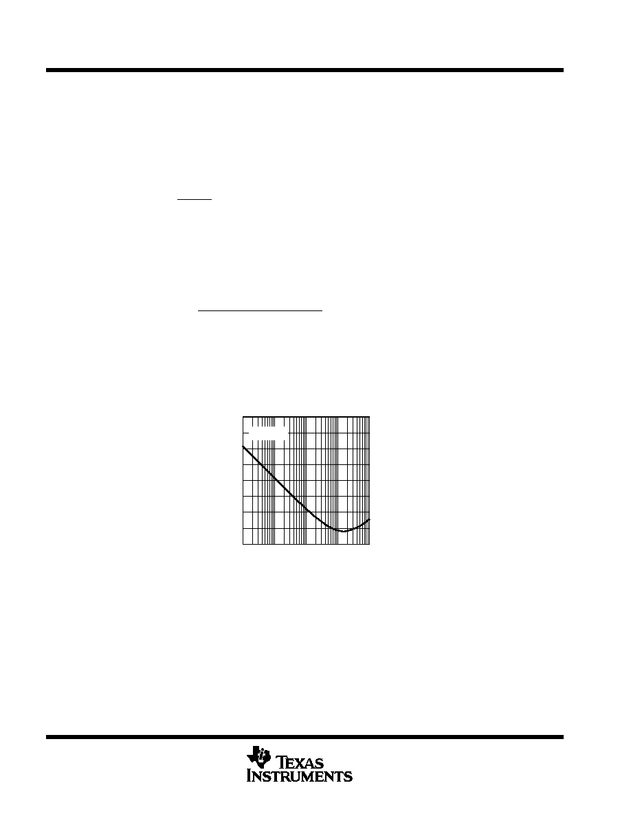
NOISE FIGURE
vs
SOURCE RESISTANCE
Source Resistance -
Noise Figure (dB)
100
1k
10k
10
100k
f = 10 kHz
TA = 25
∞
C
Figure 44. Noise Figure vs Source Resistance
THS4051, THS4052
70-MHz HIGH-SPEED AMPLIFIERS
SLOS238C≠ MAY 1999 ≠ REVISED MAY 2000
17
POST OFFICE BOX 655303
∑
DALLAS, TEXAS 75265
APPLICATION INFORMATION
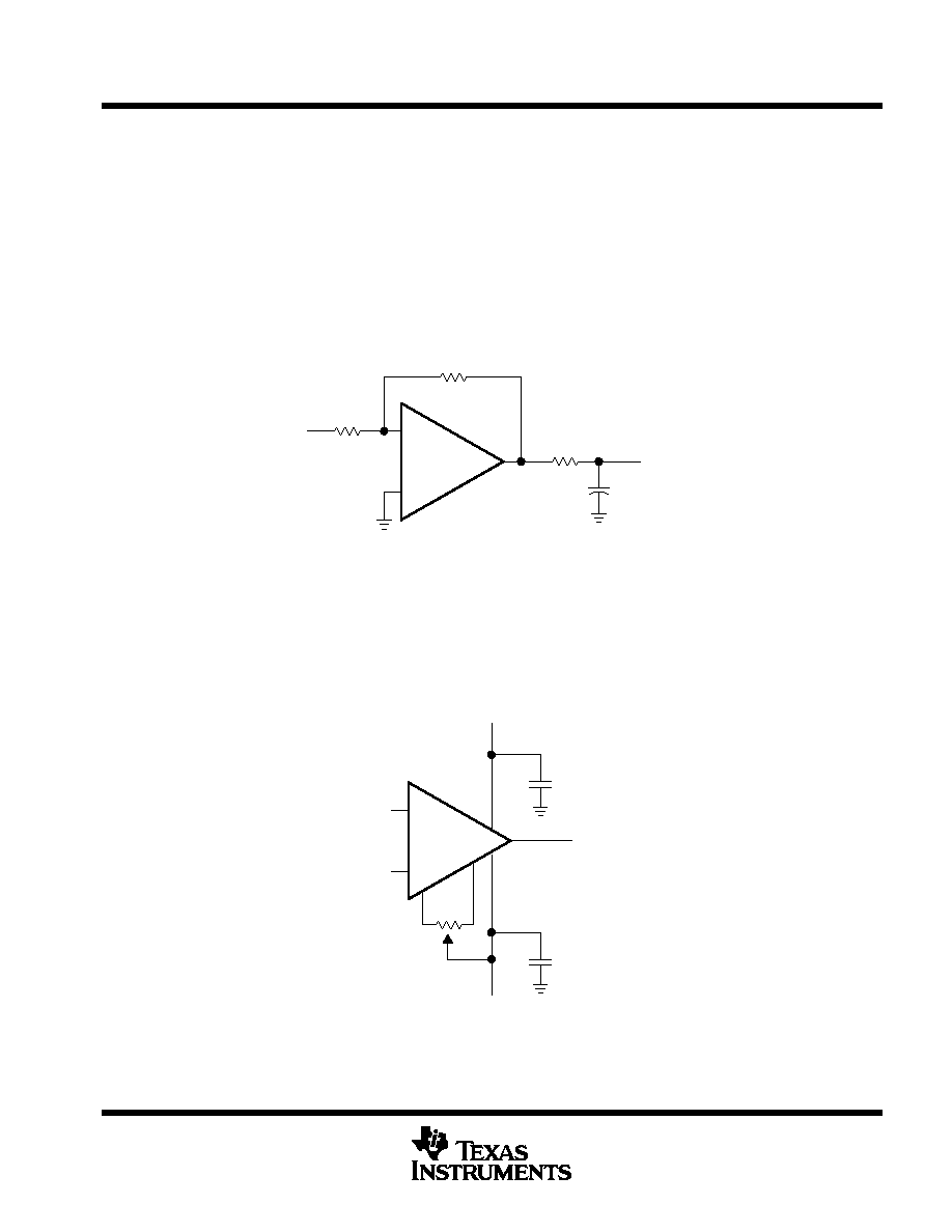
driving a capacitive load
Driving capacitive loads with high performance amplifiers is not a problem as long as certain precautions are
taken. The first is to realize that the THS405x has been internally compensated to maximize its bandwidth and
slew rate performance. When the amplifier is compensated in this manner, capacitive loading directly on the
output will decrease the device's phase margin leading to high frequency ringing or oscillations. Therefore, for
capacitive loads of greater than 10 pF, it is recommended that a resistor be placed in series with the output of
the amplifier, as shown in Figure 45. A minimum value of 20
should work well for most applications. For
example, in 75-
transmission systems, setting the series resistor value to 75
both isolates any capacitance
loading and provides the proper line impedance matching at the source end.
+
_
THS405x
CLOAD
1 k
Input
Output
1 k
20
Figure 45. Driving a Capacitive Load
offset nulling
The THS405x has very low input offset voltage for a high-speed amplifier. However, if additional correction is
required, an offset nulling function has been provided on the THS4051. The input offset can be adjusted by
placing a potentiometer between terminals 1 and 8 of the device and tying the wiper to the negative supply. This
is shown in Figure 46.
_
+
THS4051
VCC ≠
VCC+
0.1
µ
F
0.1
µ
F
10 k
Figure 46. Offset Nulling Schematic
THS4051, THS4052
70-MHz HIGH-SPEED AMPLIFIERS
SLOS238C≠ MAY 1999 ≠ REVISED MAY 2000
18
POST OFFICE BOX 655303
∑
DALLAS, TEXAS 75265
APPLICATION INFORMATION
offset voltage
The output offset voltage, (V
OO
) is the sum of the input offset voltage (V
IO
) and both input bias currents (I
IB
) times
the corresponding gains. The following schematic and formula can be used to calculate the output offset
voltage:
V
OO
+
V
IO
1
)
R
F
R
G
"
I
IB
)
R
S
1
)
R
F
R
G
"
I
IB≠
R
F
+
≠
VI
+
RG
RS
RF
IIB≠
VO
IIB+
Figure 47. Output Offset Voltage Model
optimizing unity gain response
Internal frequency compensation of the THS405x was selected to provide very wideband performance yet still
maintain stability when operated in a noninverting unity gain configuration. When amplifiers are compensated
in this manner there is usually peaking in the closed loop response and some ringing in the step response for
very fast input edges, depending upon the application. This is because a minimum phase margin is maintained
for the G=+1 configuration. For optimum settling time and minimum ringing, a feedback resistor of 620
should
be used as shown in Figure 48. Additional capacitance can also be used in parallel with the feedback resistance
if even finer optimization is required.
_
+
THS406x
620
Input
Output
Figure 48. Noninverting, Unity Gain Schematic

THS4051, THS4052
70-MHz HIGH-SPEED AMPLIFIERS
SLOS238C≠ MAY 1999 ≠ REVISED MAY 2000
19
POST OFFICE BOX 655303
∑
DALLAS, TEXAS 75265
APPLICATION INFORMATION
general configurations
When receiving low-level signals, limiting the bandwidth of the incoming signals into the system is often
required. The simplest way to accomplish this is to place an RC filter at the noninverting terminal of the amplifier
(see Figure 49).
VI
VO
C1
+
≠
RG
RF
R1
f
≠3dB
+
1
2
p
R1C1
V
O
V
I
+
1
)
R
F
R
G
1
1
)
sR1C1
Figure 49. Single-Pole Low-Pass Filter
If even more attenuation is needed, a multiple pole filter is required. The Sallen-Key filter can be used for this
task. For best results, the amplifier should have a bandwidth that is 8 to 10 times the filter frequency bandwidth.
Failure to do this can result in phase shift of the amplifier.
VI
C2
R2
R1
C1
RF
RG
R1 = R2 = R
C1 = C2 = C
Q = Peaking Factor
(Butterworth Q = 0.707)
(
=
1
Q
2 ≠
)
RG
RF
_
+
f
≠3dB
+
1
2
p
RC
Figure 50. 2-Pole Low-Pass Sallen-Key Filter

THS4051, THS4052
70-MHz HIGH-SPEED AMPLIFIERS
SLOS238C≠ MAY 1999 ≠ REVISED MAY 2000
20
POST OFFICE BOX 655303
∑
DALLAS, TEXAS 75265
APPLICATION INFORMATION
circuit layout considerations
To achieve the levels of high frequency performance of the THS405x, follow proper printed-circuit board high
frequency design techniques. A general set of guidelines is given below. In addition, a THS405x evaluation
board is available to use as a guide for layout or for evaluating the device performance.
D
Ground planes ≠ It is highly recommended that a ground plane be used on the board to provide all
components with a low inductive ground connection. However, in the areas of the amplifier inputs and
output, the ground plane can be removed to minimize the stray capacitance.
D
Proper power supply decoupling ≠ Use a 6.8-
µ
F tantalum capacitor in parallel with a 0.1-
µ
F ceramic
capacitor on each supply terminal. It may be possible to share the tantalum among several amplifiers
depending on the application, but a 0.1-
µ
F ceramic capacitor should always be used on the supply terminal
of every amplifier. In addition, the 0.1-
µ
F capacitor should be placed as close as possible to the supply
terminal. As this distance increases, the inductance in the connecting trace makes the capacitor less
effective. The designer should strive for distances of less than 0.1 inches between the device power
terminals and the ceramic capacitors.
D
Sockets ≠ Sockets are not recommended for high-speed operational amplifiers. The additional lead
inductance in the socket pins will often lead to stability problems. Surface-mount packages soldered directly
to the printed-circuit board is the best implementation.
D
Short trace runs/compact part placements ≠ Optimum high frequency performance is achieved when stray
series inductance has been minimized. To realize this, the circuit layout should be made as compact as
possible, thereby minimizing the length of all trace runs. Particular attention should be paid to the inverting
input of the amplifier. Its length should be kept as short as possible. This will help to minimize stray
capacitance at the input of the amplifier.
D
Surface-mount passive components ≠ Using surface-mount passive components is recommended for high
frequency amplifier circuits for several reasons. First, because of the extremely low lead inductance of
surface-mount components, the problem with stray series inductance is greatly reduced. Second, the small
size of surface-mount components naturally leads to a more compact layout thereby minimizing both stray
inductance and capacitance. If leaded components are used, it is recommended that the lead lengths be
kept as short as possible.
general PowerPAD
TM
design considerations
The THS405x is available packaged in a thermally-enhanced DGN package, which is a member of the
PowerPAD
TM
family of packages. This package is constructed using a downset leadframe upon which the die
is mounted [see Figure 51(a) and Figure 51(b)]. This arrangement results in the lead frame being exposed as
a thermal pad on the underside of the package [see Figure 51(c)]. Because this thermal pad has direct thermal
contact with the die, excellent thermal performance can be achieved by providing a good thermal path away
from the thermal pad.
The PowerPAD
TM
package allows for both assembly and thermal management in one manufacturing operation.
During the surface-mount solder operation (when the leads are being soldered), the thermal pad can also be
soldered to a copper area underneath the package. Through the use of thermal paths within this copper area,
heat can be conducted away from the package into either a ground plane or other heat dissipating device.
The PowerPAD
TM
package represents a breakthrough in combining the small area and ease of assembly of the
surface mount with the, heretofore, awkward mechanical methods of heatsinking.
THS4051, THS4052
70-MHz HIGH-SPEED AMPLIFIERS
SLOS238C≠ MAY 1999 ≠ REVISED MAY 2000
21
POST OFFICE BOX 655303
∑
DALLAS, TEXAS 75265
APPLICATION INFORMATION
general PowerPAD
TM
design considerations (continued)
DIE
Side View (a)
End View (b)
Bottom View (c)
DIE
Thermal
Pad
NOTE A: The thermal pad is electrically isolated from all terminals in the package.
Figure 51. Views of Thermally Enhanced DGN Package
Although there are many ways to properly heatsink this device, the following steps illustrate the recommended
approach.
Thermal pad area (68 mils x 70 mils) with 5 vias
(Via diameter = 13 mils)
Figure 52. PowerPAD
TM
PCB Etch and Via Pattern
1.
Prepare the PCB with a top side etch pattern as shown in Figure 52. There should be etch for the leads as
well as etch for the thermal pad.
2.
Place five holes in the area of the thermal pad. These holes should be 13 mils in diameter. Keep them small
so that solder wicking through the holes is not a problem during reflow.
3.
Additional vias may be placed anywhere along the thermal plane outside of the thermal pad area. This helps
dissipate the heat generated by the THS405xDGN IC. These additional vias may be larger than the 13-mil
diameter vias directly under the thermal pad. They can be larger because they are not in the thermal pad
area to be soldered so that wicking is not a problem.
4.
Connect all holes to the internal ground plane.
5.
When connecting these holes to the ground plane,
do not use the typical web or spoke via connection
methodology. Web connections have a high thermal resistance connection that is useful for slowing the heat
transfer during soldering operations. This makes the soldering of vias that have plane connections easier.
In this application, however, low thermal resistance is desired for the most efficient heat transfer. Therefore,
the holes under the THS405xDGN package should make their connection to the internal ground plane with
a complete connection around the entire circumference of the plated-through hole.
6.
The top-side solder mask should leave the terminals of the package and the thermal pad area with its five
holes exposed. The bottom-side solder mask should cover the five holes of the thermal pad area. This
prevents solder from being pulled away from the thermal pad area during the reflow process.
7.
Apply solder paste to the exposed thermal pad area and all of the IC terminals.
8.
With these preparatory steps in place, the THS405xDGN IC is simply placed in position and run through
the solder reflow operation as any standard surface-mount component. This results in a part that is properly
installed.

THS4051, THS4052
70-MHz HIGH-SPEED AMPLIFIERS
SLOS238C≠ MAY 1999 ≠ REVISED MAY 2000
22
POST OFFICE BOX 655303
∑
DALLAS, TEXAS 75265
APPLICATION INFORMATION
general PowerPAD
TM
design considerations (continued)
The actual thermal performance achieved with the THS405xDGN in its PowerPAD
TM
package depends on the
application. In the example above, if the size of the internal ground plane is approximately 3 inches
◊
3 inches,
then the expected thermal coefficient,
JA
,
is
about 58.4
∞
C/W. For comparison, the non-PowerPAD
TM
version
of the THS405x IC (SOIC) is shown. For a given
JA
, the maximum power dissipation is shown in Figure 53 and
is calculated by the following formula:
P
D
+
T
MAX
≠T
A
q
JA
Where:
P
D
= Maximum power dissipation of THS405x IC (watts)
T
MAX
= Absolute maximum junction temperature (150
∞
C)
T
A
= Free-ambient air temperature (
∞
C)
JA
=
JC
+
CA
JC
= Thermal coefficient from junction to case
CA
= Thermal coefficient from case to ambient air (
∞
C/W)
DGN Package
JA = 58.4
∞
C/W
2 oz. Trace And Copper Pad
With Solder
DGN Package
JA = 158
∞
C/W
2 oz. Trace And
Copper Pad
Without Solder
SOIC Package
High-K Test PCB
JA = 98
∞
C/W
TJ = 150
∞
C
SOIC Package
Low-K Test PCB
JA = 167
∞
C/W
2
1.5
1
0
≠40
≠20
0
20
40
Maximum Power Dissipation ≠ W
2.5
3
MAXIMUM POWER DISSIPATION
vs
FREE-AIR TEMPERATURE
3.5
60
80
100
0.5
TA ≠ Free-Air Temperature ≠
∞
C
NOTE A: Results are with no air flow and PCB size = 3"
◊
3"
Figure 53. Maximum Power Dissipation vs Free-Air Temperature
More complete details of the PowerPAD
TM
installation process and thermal management techniques can be
found in the Texas Instruments Technical Brief,
PowerPAD
TM
Thermally Enhanced Package. This document can
be found at the TI web site (www.ti.com) by searching on the key word PowerPAD
TM
. The document can also
be ordered through your local TI sales office. Refer to literature number SLMA002 when ordering.
THS4051, THS4052
70-MHz HIGH-SPEED AMPLIFIERS
SLOS238C≠ MAY 1999 ≠ REVISED MAY 2000
23
POST OFFICE BOX 655303
∑
DALLAS, TEXAS 75265
APPLICATION INFORMATION
general PowerPAD
TM
design considerations (continued)
The next consideration is the package constraints. The two sources of heat within an amplifier are quiescent
power and output power. The designer should never forget about the quiescent heat generated within the
device, especially devices with multiple amplifiers. Because these devices have linear output stages (Class
A-B), most of the heat dissipation is at low output voltages with high output currents. Figure 54 to Figure 57 show
this effect, along with the quiescent heat, with an ambient air temperature of 50
∞
C. Obviously, as the ambient
temperature increases, the limit lines shown will drop accordingly. The area under each respective limit line is
considered the safe operating area. Any condition above this line will exceed the amplifier's limits and failure
may result. When using V
CC
=
±
5 V, there is generally not a heat problem, even with SOIC packages. But, when
using V
CC
=
±
15 V, the SOIC package is severely limited in the amount of heat it can dissipate. The other key
factor when looking at these graphs is how the devices are mounted on the PCB. The PowerPAD
TM
devices are
extremely useful for heat dissipation. But, the device should always be soldered to a copper plane to fully use
the heat dissipation properties of the PowerPAD
TM
. The SOIC package, on the other hand, is highly dependent
on how it is mounted on the PCB. As more trace and copper area is placed around the device,
JA
decreases
and the heat dissipation capability increases. The currents and voltages shown in these graphs are for the total
package. For the dual amplifier package (THS4052), the sum of the RMS output currents and voltages should
be used to choose the proper package. The graphs shown assume that both amplifier's outputs are identical.
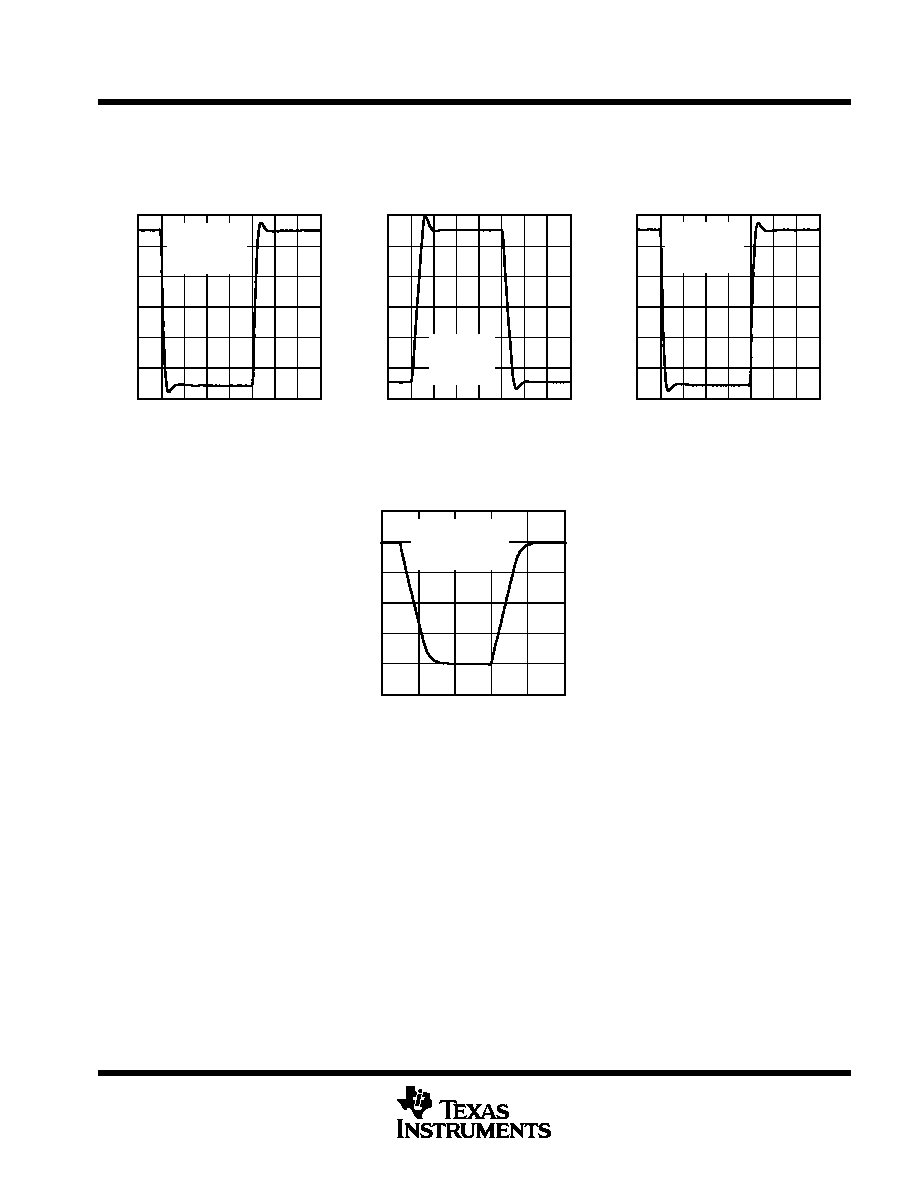
Figure 54
Package With
JA < = 120
∞
C/W
SO-8 Package
JA = 167
∞
C/W
Low-K Test PCB
VCC =
±
5 V
Tj = 150
∞
C
TA = 50
∞
C
100
80
40
0
0
1
2
3
≠ Maximum RMS Output Current ≠ mA
140
180
200
4
5
160
120
60
20
| VO | ≠ RMS Output Voltage ≠ V
I O||
Maximum Output
Current Limit Line
THS4051
MAXIMUM RMS OUTPUT CURRENT
vs
RMS OUTPUT VOLTAGE DUE TO THERMAL LIMITS
Safe Operating
Area
Figure 55
100
10
0
3
6
9
1000
12
15
Maximum Output
Current Limit Line
SO-8 Package
JA = 167
∞
C/W
Low-K Test PCB
SO-8 Package
JA = 98
∞
C/W
High-K Test PCB
TJ = 150
∞
C
TA = 50
∞
C
| VO | ≠ RMS Output Voltage ≠ V
≠ Maximum RMS Output Current ≠ mA
I O||
VCC =
±
15 V
DGN Package
JA = 58.4
∞
C/W
THS4051
MAXIMUM RMS OUTPUT CURRENT
vs
RMS OUTPUT VOLTAGE DUE TO THERMAL LIMITS
Safe Operating
Area

THS4051, THS4052
70-MHz HIGH-SPEED AMPLIFIERS
SLOS238C≠ MAY 1999 ≠ REVISED MAY 2000
24
POST OFFICE BOX 655303
∑
DALLAS, TEXAS 75265
APPLICATION INFORMATION
general PowerPAD
TM
design considerations (continued)
Figure 56
Package With
JA
60
∞
C/W
SO-8 Package
JA = 98
∞
C/W
High-K Test PCB
VCC =
±
5 V
TJ = 150
∞
C
TA = 50
∞
C
Both Channels
100
80
40
0
0
1
2
3
≠ Maximum RMS Output Current ≠ mA
140
180
200
4
5
160
120
60
20
| VO | ≠ RMS Output Voltage ≠ V
I O||
Maximum Output
Current Limit Line
THS4052
MAXIMUM RMS OUTPUT CURRENT
vs
RMS OUTPUT VOLTAGE DUE TO THERMAL LIMITS
SO-8 Package
JA = 167
∞
C/W
Low-K Test PCB
Safe Operating Area
Figure 57
100
10
0
3
6
9
1000
12
15
Maximum Output
Current Limit Line
| VO | ≠ RMS Output Voltage ≠ V
≠ Maximum RMS Output Current ≠ mA
I O||
VCC =
±
15 V
TJ = 150
∞
C
TA = 50
∞
C
Both Channels
THS4052
MAXIMUM RMS OUTPUT CURRENT
vs
RMS OUTPUT VOLTAGE DUE TO THERMAL LIMITS
1
SO-8 Package
JA = 167
∞
C/W
Low-K Test PCB
DGN Package
JA = 58.4
∞
C/W
Safe Operating Area
SO-8 Package
JA = 98
∞
C/W
High-K Test PCB

THS4051, THS4052
70-MHz HIGH-SPEED AMPLIFIERS
SLOS238C≠ MAY 1999 ≠ REVISED MAY 2000
25
POST OFFICE BOX 655303
∑
DALLAS, TEXAS 75265
APPLICATION INFORMATION
evaluation board
An evaluation board is available for the THS4051 (literature number SLOP220) and THS4052 (literature number
SLOP234). This board has been configured for very low parasitic capacitance in order to realize the full
performance of the amplifier. A schematic of the evaluation board is shown in Figure 58. The circuitry has been
designed so that the amplifier may be used in either an inverting or noninverting configuration. For more
information, please refer to the
THS4051 EVM User's Guide or the THS4052 EVM User's Guide. To order the
evaluation board, contact your local TI sales office or distributor.
_
+
THS4051
VCC ≠
VCC+
C1
6.8
µ
F
C4
0.1
µ
F
C2
6.8
µ
F
C5
0.1
µ
F
R4
2 k
R2
2 k
R3
49.9
R5
49.9
R1
49.9
IN ≠
IN +
NULL
OUT
NULL
+
+
Figure 58. THS4051 Evaluation Board

THS4051, THS4052
70-MHz HIGH-SPEED AMPLIFIERS
SLOS238C≠ MAY 1999 ≠ REVISED MAY 2000
26
POST OFFICE BOX 655303
∑
DALLAS, TEXAS 75265
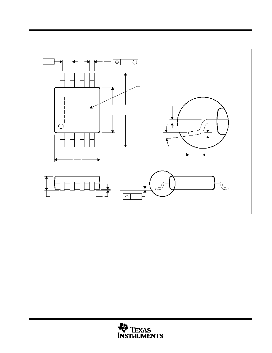
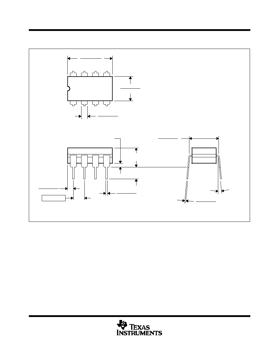
MECHANICAL INFORMATION
D (R-PDSO-G**)
PLASTIC SMALL-OUTLINE PACKAGE
14 PIN SHOWN
4040047 / D 10/96
0.228 (5,80)
0.244 (6,20)
0.069 (1,75) MAX
0.010 (0,25)
0.004 (0,10)
1
14
0.014 (0,35)
0.020 (0,51)
A
0.157 (4,00)
0.150 (3,81)
7
8
0.044 (1,12)
0.016 (0,40)
Seating Plane
0.010 (0,25)
PINS **
0.008 (0,20) NOM
A MIN
A MAX
DIM
Gage Plane
0.189
(4,80)
(5,00)
0.197
8
(8,55)
(8,75)
0.337
14
0.344
(9,80)
16
0.394
(10,00)
0.386
0.004 (0,10)
M
0.010 (0,25)
0.050 (1,27)
0
∞
≠ 8
∞
NOTES: A. All linear dimensions are in inches (millimeters).
B. This drawing is subject to change without notice.
C. Body dimensions do not include mold flash or protrusion, not to exceed 0.006 (0,15).
D. Falls within JEDEC MS-012
THS4051, THS4052
70-MHz HIGH-SPEED AMPLIFIERS
SLOS238C≠ MAY 1999 ≠ REVISED MAY 2000
27
POST OFFICE BOX 655303
∑
DALLAS, TEXAS 75265
MECHANICAL INFORMATION
DGN (S-PDSO-G8)
PowerPAD
TM
PLASTIC SMALL-OUTLINE PACKAGE
0,69
0,41
0,25
Thermal Pad
(See Note D)
0,15 NOM
Gage Plane
4073271/A 01/98
4,98
0,25
5
3,05
4,78
2,95
8
4
3,05
2,95
1
0,38
0,15
0,05
1,07 MAX
Seating Plane
0,10
0,65
M
0,25
0
∞
≠ 6
∞
NOTES: A. All linear dimensions are in millimeters.
B. This drawing is subject to change without notice.
C. Body dimensions include mold flash or protrusions.
D. The package thermal performance may be enhanced by attaching an external heat sink to the thermal pad. This pad is electrically
and thermally connected to the backside of the die and possibly selected leads.
E. Falls within JEDEC MO-187
PowerPAD is a trademark of Texas Instruments.
THS4051, THS4052
70-MHz HIGH-SPEED AMPLIFIERS
SLOS238C≠ MAY 1999 ≠ REVISED MAY 2000
28
POST OFFICE BOX 655303
∑
DALLAS, TEXAS 75265
MECHANICAL INFORMATION
FK (S-CQCC-N**)
LEADLESS CERAMIC CHIP CARRIER
4040140 / D 10/96
28 TERMINAL SHOWN
B
0.358
(9,09)
MAX
(11,63)
0.560
(14,22)
0.560
0.458
0.858
(21,8)
1.063
(27,0)
(14,22)
A
NO. OF
MIN
MAX
0.358
0.660
0.761
0.458
0.342
(8,69)
MIN
(11,23)
(16,26)
0.640
0.739
0.442
(9,09)
(11,63)
(16,76)
0.962
1.165
(23,83)
0.938
(28,99)
1.141
(24,43)
(29,59)
(19,32)
(18,78)
**
20
28
52
44
68
84
0.020 (0,51)
TERMINALS
0.080 (2,03)
0.064 (1,63)
(7,80)
0.307
(10,31)
0.406
(12,58)
0.495
(12,58)
0.495
(21,6)
0.850
(26,6)
1.047
0.045 (1,14)
0.045 (1,14)
0.035 (0,89)
0.035 (0,89)
0.010 (0,25)
12
13
14
15
16
18
17
11
10
8
9
7
5
4
3
2
0.020 (0,51)
0.010 (0,25)
6
1
28
26
27
19
21
B SQ
A SQ
22
23
24
25
20
0.055 (1,40)
0.045 (1,14)
0.028 (0,71)
0.022 (0,54)
0.050 (1,27)
NOTES: A. All linear dimensions are in inches (millimeters).
B. This drawing is subject to change without notice.
C. This package can be hermetically sealed with a metal lid.
D. The terminals are gold plated.
E. Falls within JEDEC MS-004
THS4051, THS4052
70-MHz HIGH-SPEED AMPLIFIERS
SLOS238C≠ MAY 1999 ≠ REVISED MAY 2000
29
POST OFFICE BOX 655303
∑
DALLAS, TEXAS 75265
MECHANICAL INFORMATION
JG (R-GDIP-T8)
CERAMIC DUAL-IN-LINE PACKAGE
0.310 (7,87)
0.290 (7,37)
0.014 (0,36)
0.008 (0,20)
Seating Plane
4040107/C 08/96
5
4
0.065 (1,65)
0.045 (1,14)
8
1
0.020 (0,51) MIN
0.400 (10,20)
0.355 (9,00)
0.015 (0,38)
0.023 (0,58)
0.063 (1,60)
0.015 (0,38)
0.200 (5,08) MAX
0.130 (3,30) MIN
0.245 (6,22)
0.280 (7,11)
0.100 (2,54)
0
∞
≠15
∞
NOTES: A. All linear dimensions are in inches (millimeters).
B. This drawing is subject to change without notice.
C. This package can be hermetically sealed with a ceramic lid using glass frit.
D. Index point is provided on cap for terminal identification only on press ceramic glass frit seal only.
E. Falls within MIL-STD-1835 GDIP1-T8

IMPORTANT NOTICE
Texas Instruments and its subsidiaries (TI) reserve the right to make changes to their products or to discontinue
any product or service without notice, and advise customers to obtain the latest version of relevant information
to verify, before placing orders, that information being relied on is current and complete. All products are sold
subject to the terms and conditions of sale supplied at the time of order acknowledgment, including those
pertaining to warranty, patent infringement, and limitation of liability.
TI warrants performance of its semiconductor products to the specifications applicable at the time of sale in
accordance with TI's standard warranty. Testing and other quality control techniques are utilized to the extent
TI deems necessary to support this warranty. Specific testing of all parameters of each device is not necessarily
performed, except those mandated by government requirements.
Customers are responsible for their applications using TI components.
In order to minimize risks associated with the customer's applications, adequate design and operating
safeguards must be provided by the customer to minimize inherent or procedural hazards.
TI assumes no liability for applications assistance or customer product design. TI does not warrant or represent
that any license, either express or implied, is granted under any patent right, copyright, mask work right, or other
intellectual property right of TI covering or relating to any combination, machine, or process in which such
semiconductor products or services might be or are used. TI's publication of information regarding any third
party's products or services does not constitute TI's approval, warranty or endorsement thereof.
Copyright
©
2000, Texas Instruments Incorporated