 | –≠–ª–µ–∫—Ç—Ä–æ–Ω–Ω—ã–π –∫–æ–º–ø–æ–Ω–µ–Ω—Ç: 65HVD05 | –°–∫–∞—á–∞—Ç—å:  PDF PDF  ZIP ZIP |
Document Outline
- FEATURES
- APPLICATIONS
- DESCRIPTION
- ORDERING INFORMATION
- PACKAGE DISSIPATION RATINGS (SEE FIGURE 12 AND FIGURE 13)
- ABSOLUTE MAXIMUM RATINGS
- RECOMMENDED OPERATING CONDITIONS
- DRIVER ELECTRICAL CHARACTERISTICS
- DRIVER SWITCHING CHARACTERISTICS NIL
- RECEIVER ELECTRICAL CHARACTERISTICS
- RECEIVER SWITCHING CHARACTERISTICS
- PARAMETER MEASUREMENT INFORMATION
- EQUIVALENT INPUT AND OUTPUT SCHEMATIC DIAGRAMS
- TYPICAL CHARACTERISTICS
- APPLICATION INFORMATION

SN65HVD05, SN65HVD06, SN65HVD07
SN75HVD05, SN75HVD06, SN75HVD07
SLLS533B ≠ MAY 2002 ≠ REVISED MAY 2003
HIGH OUTPUT RS-485 TRANSCEIVERS
FEATURES
D
Minimum Differential Output Voltage of 2.5 V
Into a 54-
Load
D
Open-Circuit, Short-Circuit, and Idle-Bus
Failsafe Receiver
D
1/8
th
Unit-Load Option Available (Up to 256
Nodes on the Bus)
D
Bus-Pin ESD Protection Exceeds 16 kV HBM
D
Driver Output Slew Rate Control Options
D
Electrically Compatible With ANSI
TIA/EIA-485-A Standard
D
Low-Current Standby Mode . . . 1
µ
A Typical
D
Glitch-Free Power-Up and Power-Down
Protection for Hot-Plugging Applications
D
Pin Compatible With Industry Standard
SN75176
APPLICATIONS
D
Data Transmission Over Long or Lossy Lines
or Electrically Noisy Environments
D
Profibus Line Interface
D
Industrial Process Control Networks
D
Point-of-Sale (POS) Networks
D
Electric Utility Metering
D
Building Automation
D
Digital Motor Control
DESCRIPTION
The SN65HVD05, SN75HVD05, SN65HVD06,
SN75HVD06, SN65HVD07, and SN75HVD07 combine
a 3-state differential line driver and differential line
receiver. They are designed for balanced data
transmission and interoperate with ANSI
TIA/EIA-485-A and ISO 8482E standard-compliant
devices. The driver is designed to provide a differential
output voltage greater than that required by these
standards for increased noise margin. The drivers and
receivers have active-high and active-low enables
respectively, which can be externally connected
together to function as direction control.
The driver differential outputs and receiver differential
inputs connect internally to form a differential input/
output (I/O) bus port that is designed to offer minimum
loading to the bus whenever the driver is disabled or not
powered. These devices feature wide positive and
negative common-mode voltage ranges, making them
suitable for party-line applications.
1
2
3
4
8
7
6
5
R
RE
DE
D
V
CC
B
A
GND
D OR P PACKAGE
(TOP VIEW)
0
0.5
1
1.5
2
2.5
3
3.5
4
4.5
5
0
20
40
60
80
100
120
≠ Differential Output V
oltage
≠
V
DIFFERENTIAL OUTPUT VOLTAGE
vs
DIFFERENTIAL OUTPUT CURRENT
V
O
IOD ≠ Differential Output Current ≠ mA
60
Load
Line
30
Load
Line
TA = 25
∞
C
DE at VCC
D at VCC
VCC = 5 V
1
2
3
4
6
7
A
B
R
RE
DE
D
LOGIC DIAGRAM
(POSITIVE LOGIC)
PRODUCTION DATA information is current as of publication date. Products
conform to specifications per the terms of Texas Instruments standard warranty.
Production processing does not necessarily include testing of all parameters.
Please be aware that an important notice concerning availability, standard warranty, and use in critical applications of Texas Instruments
semiconductor products and disclaimers thereto appears at the end of this data sheet.
www.ti.com
Copyright
2002≠2003, Texas Instruments Incorporated
SN65HVD05, SN65HVD06, SN65HVD07
SN75HVD05, SN75HVD06, SN75HVD07
SLLS533B ≠ MAY 2002 ≠ REVISED MAY 2003
www.ti.com
2
These devices have limited built-in ESD protection. The leads should be shorted together or the device placed in conductive foam during
storage or handling to prevent electrostatic damage to the MOS gates.
ORDERING INFORMATION
(1)
MARKED AS
SIGNALING
RATE
UNIT
LOAD
DRIVER
OUTPUT SLOPE
CONTROL
TA
PART NUMBER(2)
PLASTIC
DUAL-IN-LINE
PACKAGE
(PDIP)
SMALL OUTLINE
IC (SOIC)
PACKAGE
40 Mbps
1/2
No
SN65HVD05D
SN65HVD05P
65HVD05
VP05
10 Mbps
1/8
Yes
≠40
∞
C to 85
∞
C
SN65HVD06D
SN65HVD06P
65HVD06
VP06
1 Mbps
1/8
Yes
40 C to 85 C
SN65HVD07D
SN65HVD07P
65HVD07
VP07
40 Mbps
1/2
No
SN75HVD05D
SN75HVD05P
75HVD05
VN05
10 Mbps
1/8
Yes
≠0
∞
C to 70
∞
C
SN75HVD06D
SN75HVD06P
75HVD06
VN06
1 Mbps
1/8
Yes
0 C to 70 C
SN75HVD07D
SN75HVD07P
75HVD07
VN07
(1) For the most current specification and package information, refer to our web site at www.ti.com.
(2) The D package is available taped and reeled. Add an R suffix to the device type (i.e., SN65HVD05DR).
PACKAGE DISSIPATION RATINGS (SEE FIGURE 12 AND FIGURE 13)
PACKAGE
TA
25
∞
C
POWER RATING
DERATING FACTOR(1)
ABOVE TA = 25
∞
C
TA = 70
∞
C
POWER RATING
TA = 85
∞
C POWER
RATING
D(2)
710 mW
5.7 mW/
∞
C
455 mW
369 mW
D(3)
1282 mW
10.3 mW/
∞
C
821 mW
667 mW
P
1000 mW
8.0 mW/
∞
C
640 mW
520 mW
(1) This is the inverse of the junction-to-ambient thermal resistance when board-mounted and with no air flow.
(2) Tested in accordance with the Low-K thermal metric definitions of EIA/JESD51-3
(3) Tested in accordance with the High-K thermal metric definitions of EIA/JESD51-7
ABSOLUTE MAXIMUM RATINGS
over operating free-air temperature range unless otherwise noted(1) (2)
SN65HVD05, SN65HVD06, SN65HVD07
SN75HVD05, SN75HVD06, SN75HVD07
Supply voltage range, VCC
≠0.3 V to 6 V
Voltage range at A or B
≠9 V to 14 V
Input voltage range at D, DE, R or RE
≠0.5 V to VCC + 0.5 V
Voltage input range, transient pulse, A and B, through 100
(see Figure 11)
≠50 V to 50 V
Human body model(3)
A, B, and GND
16 kV
Electrostatic discharge
Human body model(3)
All pins
4 kV
Electrostatic discharge
Charged-device model(4)
All pins
1 kV
Continuous total power dissipation
See Dissipation Rating Table
Storage temperature range, Tstg
≠65
∞
C to 150
∞
C
Lead temperature 1,6 mm (1/16 inch) from case for 10 seconds
260
∞
C
(1) Stresses beyond those listed under "absolute maximum ratings" may cause permanent damage to the device. These are stress ratings only, and
functional operation of the device at these or any other conditions beyond those indicated under "recommended operating conditions" is not
implied. Exposure to absolute-maximum-rated conditions for extended periods may affect device reliability.
(2) All voltage values, except differential I/O bus voltages, are with respect to network ground terminal.
(3) Tested in accordance with JEDEC Standard 22, Test Method A114-A.
(4) Tested in accordance with JEDEC Standard 22, Test Method C101.

SN65HVD05, SN65HVD06, SN65HVD07
SN75HVD05, SN75HVD06, SN75HVD07
SLLS533B ≠ MAY 2002 ≠ REVISED MAY 2003
www.ti.com
3
RECOMMENDED OPERATING CONDITIONS
MIN
NOM
MAX
UNIT
Supply voltage, VCC
4.5
5.5
V
Voltage at any bus terminal (separately or common mode) VI or VIC
≠7(1)
12
V
High-level input voltage, VIH
D, DE, RE
2
V
Low-level input voltage, VIL
D, DE, RE
0.8
V
Differential input voltage, VID (see Figure 7)
≠12
12
V
High level output current I
Driver
≠100
mA
High-level output current, IOH
Receiver
≠8
mA
Low level output current I
Driver
100
mA
Low-level output current, IOL
Receiver
8
mA
SN65HVD05
SN65HVD06
≠40
85
∞
C
Operating free air temperature T
SN65HVD07
40
85
C
Operating free-air temperature, TA
SN75HVD05
SN75HVD06
0
70
∞
C
SN75HVD07
0
70
C
(1) The algebraic convention, in which the least positive (most negative) limit is designated as minimum is used in this data sheet.
DRIVER ELECTRICAL CHARACTERISTICS
over operating free-air temperature range unless otherwise noted(1)
PARAMETER
TEST CONDITIONS
MIN
TYP(1)
MAX
UNIT
VIK
Input clamp voltage
II = ≠18 mA
≠1.5
V
No Load
VCC
|VOD|
Differential output voltage
RL = 54
, See Figure 1
2.5
V
|VOD|
Differential out ut voltage
Vtest = ≠7 V to 12 V, See Figure 2
2.2
V
|VOD|
Change in magnitude of differential
output voltage
See Figure 1 and Figure 2
≠0.2
0.2
V
VOC(SS)
Steady-state common-mode output
voltage
See Figure 3
2.2
3.3
V
VOC(SS)
Change in steady-state
common-mode output voltage
See Figure 3
≠0.1
0.1
V
Peak to peakcommon
HVD05
600
VOC(PP)
Peak-to-peak common-
mode output voltage
HVD06
See Figure 3
500
mV
VOC(PP)
mode output voltage
HVD07
See Figure 3
900
mV
IOZ
High-impedance output current
See receiver input currents
II
Input current
D
≠100
0
µ
A
II
Input current
DE
0
100
µ
A
IOS
Short-circuit output current
≠7 V
VO
12 V
≠250
250
mA
C(diff)
Differential output capacitance
VID = 0.4 sin (4E6
t) + 0.5 V, DE at 0 V
16
pF
RE at VCC,
D & DE at VCC, No load
Receiver disabled and
driver enabled
9
15
mA
ICC
Supply current
RE at VCC, D at VCC
DE at 0 V, No load
Receiver disabled and
driver disabled
(standby)
1
5
µ
A
RE at 0 V,
D & DE at VCC, No load
Receiver enabled and
driver enabled
9
15
mA
(1) All typical values are at 25
∞
C and with a 5-V supply.

SN65HVD05, SN65HVD06, SN65HVD07
SN75HVD05, SN75HVD06, SN75HVD07
SLLS533B ≠ MAY 2002 ≠ REVISED MAY 2003
www.ti.com
4
DRIVER SWITCHING CHARACTERISTICS NIL
over operating free-air temperature range unless otherwise noted
PARAMETER
TEST
CONDITIONS
MIN
TYP(1)
MAX
UNIT
HVD05
6.5
11
tPLH
Propagation delay time, low-to-high-level output
HVD06
27
40
ns
tPLH
Pro agation delay time, low to high level out ut
HVD07
250
400
ns
HVD05
6.5
11
tPHL
Propagation delay time, high-to-low-level output
HVD06
27
40
ns
tPHL
Pro agation delay time, high to low level out ut
HVD07
250
400
ns
HVD05
RL = 54
,
2.7
3.6
6
tr
Differential output signal rise time
HVD06
RL = 54
,
CL = 50 pF,
18
28
55
ns
tr
Differential out ut signal rise time
HVD07
CL 50 F,
See Figure 4
150
300
450
ns
HVD05
2.7
3.6
6
tf
Differential output signal fall time
HVD06
18
28
55
ns
tf
Differential out ut signal fall time
HVD07
150
300
450
ns
HVD05
2
tsk(p)
Pulse skew (|tPHL ≠ tPLH|)
HVD06
2.5
ns
tsk( )
Pulse skew (|tPHL tPLH|)
HVD07
10
ns
HVD05
3.5
tsk(pp)(2)
Part-to-part skew
HVD06
14
ns
tsk( )(2)
Part to art skew
HVD07
100
ns
HVD05
25
tPZH1
Propagation delay time, high-impedance-to-high-level output
HVD06
45
ns
tPZH1
Pro agation delay time, high im edance to high level out ut
HVD07
RE at 0 V,
RL 110
250
ns
HVD05
RL = 110
,
See Figure 5
25
tPHZ
Propagation delay time, high-level-to-high-impedance output
HVD06
See Figure 5
60
ns
tPHZ
Pro agation delay time, high level to high im edance out ut
HVD07
250
ns
HVD05
15
tPZL1
Propagation delay time, high-impedance-to-low-level output
HVD06
45
ns
tPZL1
Pro agation delay time, high im edance to low level out ut
HVD07
RE at 0 V,
RL 110
200
ns
HVD05
RL = 110
,
See Figure 6
14
tPLZ
Propagation delay time, low-level-to-high-impedance output
HVD06
See Figure 6
90
ns
tPLZ
Pro agation delay time, low level to high im edance out ut
HVD07
550
ns
tPZH2
Propagation delay time, standby-to-high-level output
RL = 110
,
RE at 3 V,
See Figure 5
6
µ
s
tPZL2
Propagation delay time, standby-to-low-level output
RL = 110
,
RE at 3 V,
See Figure 6
6
µ
s
(1) All typical values are at 25
∞
C and with a 5-V supply.
(2) tsk(pp) is the magnitude of the difference in propagation delay times between any specified terminals of two devices when both devices operate
with the same supply voltages, at the same temperature, and have identical packages and test circuits.
SN65HVD05, SN65HVD06, SN65HVD07
SN75HVD05, SN75HVD06, SN75HVD07
SLLS533B ≠ MAY 2002 ≠ REVISED MAY 2003
www.ti.com
5
RECEIVER ELECTRICAL CHARACTERISTICS
over operating free-air temperature range unless otherwise noted
PARAMETER
TEST CONDITIONS
MIN
TYP(1)
MAX
UNIT
VIT+
Positive-going input threshold
voltage
IO = ≠8 mA
≠0.01
V
VIT≠
Negative-going input threshold
voltage
IO = 8 mA
≠0.2
V
Vhys
Hysteresis voltage (VIT+ ≠ VIT≠)
35
mV
VIK
Enable-input clamp voltage
II = ≠18 mA
≠1.5
V
VOH
High-level output voltage
VID = 200 mV,
IOH = ≠8 mA,
See Figure 7
4
V
VOL
Low-level output voltage
VID = ≠200 mV,
IOL = 8 mA,
See Figure 7
0.4
V
IOZ
High-impedance-state output
current
VO = 0 or VCC
RE at VCC
≠1
1
µ
A
VA or VB = 12 V
0.23
0.5
HVD05
Other input
VA or VB = 12 V,
VCC = 0 V
0.3
0.5
mA
HVD05
Other in ut
at 0 V
VA or VB = ≠7 V
≠0.4
≠0.13
mA
II
Bus input current
VA or VB = ≠7 V,
VCC = 0 V
≠0.4
≠0.15
II
Bus input current
VA or VB = 12 V
0.06
0.1
HVD06,
Other input
VA or VB = 12 V,
VCC = 0 V
0.08
0.13
mA
HVD06,
HVD07
Other in ut
at 0 V
VA or VB = ≠7 V
≠0.1
≠0.05
mA
VA or VB = ≠7 V,
VCC = 0 V
≠0.05
≠0.03
IIH
High-level input current, RE
VIH = 2 V
≠60
≠26.4
µ
A
IIL
Low-level input current, RE
VIL = 0.8 V
≠60
≠27.4
µ
A
C(diff)
Differential input capacitance
VI = 0.4 sin (4E6
t) + 0.5 V,
DE at 0 V
16
pF
RE at 0 V,
D & DE at 0 V,
No load
Receiver enabled and driver disabled
5
10
mA
ICC
Supply current
RE at VCC,
DE at 0 V,
D at VCC,
No load
Receiver disabled and driver disabled
(standby)
1
5
µ
A
RE at 0 V,
D & DE at VCC,
No load
Receiver enabled and driver enabled
9
15
mA
(1) All typical values are at 25
∞
C and with a 5-V supply.

SN65HVD05, SN65HVD06, SN65HVD07
SN75HVD05, SN75HVD06, SN75HVD07
SLLS533B ≠ MAY 2002 ≠ REVISED MAY 2003
www.ti.com
6
RECEIVER SWITCHING CHARACTERISTICS
over operating free-air temperature range unless otherwise noted
PARAMETER
TEST CONDITIONS
MIN
TYP(1)
MAX
UNIT
tPLH
Propagation delay time, low-to-high-level output 1/2 UL
HVD05
14.6
25
ns
tPHL
Propagation delay time, high-to-low-level output 1/2 UL
HVD05
14.6
25
ns
t
Propagation delay time low to high level output 1/8 UL
HVD06
55
70
ns
tPLH
Propagation delay time, low-to-high-level output 1/8 UL
HVD07
VID = ≠1.5 V to 1.5 V,
55
70
ns
t
Propagation delay time high to low level output 1/8 UL
HVD06
VID = ≠1.5 V to 1.5 V,
CL = 15 pF,
55
70
ns
tPHL
Propagation delay time, high-to-low-level output 1/8 UL
HVD07
CL 15 F,
See Figure 8
55
70
ns
HVD05
2
tsk(p)
Pulse skew (|tPHL ≠ tPLH|)
HVD06
4.5
ns
tsk( )
Pulse skew (|tPHL tPLH|)
HVD07
4.5
ns
HVD05
6.5
tsk(pp)(2)
Part-to-part skew
HVD06
14
ns
tsk( )( )
Part to art skew
HVD07
14
ns
tr
Output signal rise time
CL = 15 pF,
2
3
ns
tf
Output signal fall time
CL = 15 F,
See Figure 8
2
3
ns
tPZH1
Output enable time to high level
10
tPZL1
Output enable time to low level
CL = 15 pF,
DE at 3 V
10
ns
tPHZ
Output disable time from high level
DE at 3 V,
See Figure 9
15
ns
tPLZ
Output disable time from low level
See Figure 9
15
tPZH2
Propagation delay time, standby-to-high-level output
CL = 15 pF
,
DE at 0,
6
s
tPZL2
Propagation delay time, standby-to-low-level output
CL = 15 F
,
DE at 0,
See Figure 10
6
µ
s
(1) All typical values are at 25
∞
C and with a 5-V supply.
(2) tsk(pp) is the magnitude of the difference in propagation delay times between any specified terminals of two devices when both devices operate
with the same supply voltages, at the same temperature, and have identical packages and test circuits.

SN65HVD05, SN65HVD06, SN65HVD07
SN75HVD05, SN75HVD06, SN75HVD07
SLLS533B ≠ MAY 2002 ≠ REVISED MAY 2003
www.ti.com
7
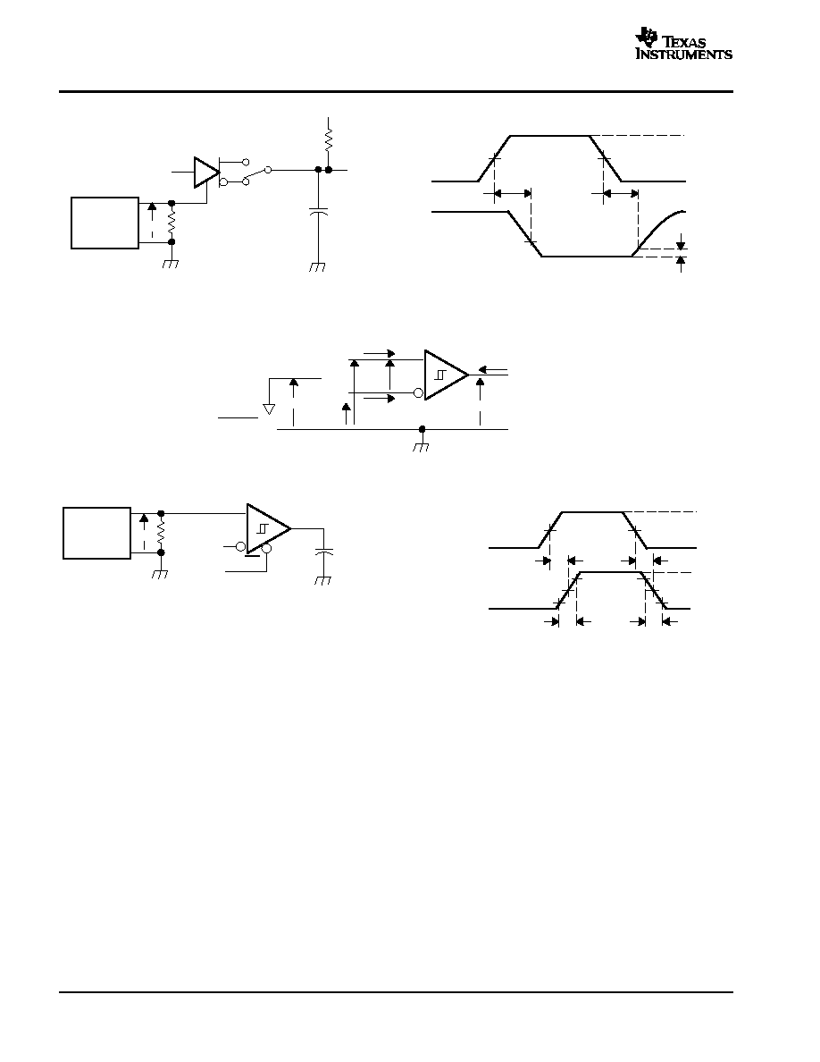
PARAMETER MEASUREMENT INFORMATION
IOA
VOD
54
±
1%
0 or 3 V
VOA
VOB
IOB
DE
VCC
II
VI
A
B
Figure 1. Driver V
OD
Test Circuit
and Voltage and Current
Definitions
60
±
1%
VOD
0 or 3 V
_
+ ≠7 V < V(test)
< 12 V
DE
VCC
A
B
D
375
±
1%
375
±
1%
Figure 2. Driver V
OD
With Common-Mode
Loading Test Circuit
VOC
27
±
1%
Input
A
B
VA
VB
VOC(PP)
VOC(SS)
VOC
27
±
1%
CL = 50 pF
±
20%
D
A
B
DE
VCC
Input: PRR = 500 kHz, 50% Duty Cycle,tr<6ns, tf<6ns, ZO = 50
CL Includes Fixture and
Instrumentation Capacitance
Figure 3. Test Circuit and Definitions for the Driver Common-Mode Output Voltage
VOD
RL = 54
±
1%
50
Generator: PRR = 500 kHz, 50% Duty Cycle, tr <6 ns, tf <6 ns, Zo = 50
tPLH
tPHL
1.5 V
1.5 V
3 V
2 V
≠2 V
90%
10%
0 V
VI
VOD
tr
tf
CL = 50 pF
±
20%
CL Includes Fixture
and Instrumentation
Capacitance
D
A
B
DE
VCC
VI
Input
Generator
90%
0 V
10%
0 V
Figure 4. Driver Switching Test Circuit and Voltage Waveforms
RL = 110
±
1%
Input
Generator
50
Generator: PRR = 100 kHz, 50% Duty Cycle, tr <6 ns, tf <6 ns, Zo = 50
3 V
S1
0.5 V
3 V
0 V
VOH
0 V
tPHZ
tPZH(1 & 2)
1.5 V
1.5 V
VI
VO
CL = 50 pF
±
20%
CL Includes Fixture
and Instrumentation
Capacitance
D
A
B
DE
VO
VI
2.3 V
Figure 5. Driver High-Level Enable and Disable Time Test Circuit and Voltage Waveforms
SN65HVD05, SN65HVD06, SN65HVD07
SN75HVD05, SN75HVD06, SN75HVD07
SLLS533B ≠ MAY 2002 ≠ REVISED MAY 2003
www.ti.com
8
Input
Generator
50
3 V
VO
S1
1.5 V
1.5 V
tPLZ
2.3 V
0.5 V
3 V
0 V
VOL
VI
VO
Generator: PRR = 100 kHz, 50% Duty Cycle, tr <6 ns, tf <6 ns, Zo = 50
RL = 110
±
1%
CL = 50 pF
±
20%
CL Includes Fixture
and Instrumentation
Capacitance
D
A
B
DE
VI
tPZL(1 & 2)
VCC
VCC
Figure 6. Driver Low-Level Output Enable and Disable Time Test Circuit and Voltage Waveforms
VID
VA
VB
IO
A
B
IB
VO
R
IA
VIC
VA + VB
2
Figure 7. Receiver Voltage and Current Definitions
Input
Generator
50
Generator: PRR = 100 kHz, 50% Duty Cycle, tr <6 ns, tf <6 ns, Zo = 50
VO
1.5 V
0 V
1.5 V
1.5 V
3 V
VOH
VOL
1.5 V
10%
1.5 V
tPLH
tPHL
tr
tf
90%
VI
VO
CL = 15 pF
±
20%
CL Includes Fixture
and Instrumentation
Capacitance
A
B
RE
VI
R
0 V
90%
10%
Figure 8. Receiver Switching Test Circuit and Voltage Waveforms

SN65HVD05, SN65HVD06, SN65HVD07
SN75HVD05, SN75HVD06, SN75HVD07
SLLS533B ≠ MAY 2002 ≠ REVISED MAY 2003
www.ti.com
9
50
Generator: PRR = 100 kHz,
50% Duty Cycle,
tr <6 ns, tf <6 ns, Zo = 50
VO
RE
VCC
0 V or 3 V
1.5 V
1.5 V
tPZH(1)
tPHZ
1.5 V
VOH ≠0.5 V
3 V
0 V
VOH
0 V
VO
CL = 15 pF
±
20%
CL Includes Fixture and
Instrumentation Capacitance
VI
DE
D
1 k
±
1%
VI
A
B
S1
D at 3 V
S1 to B
tPZL(1)
tPLZ
1.5 V
VOL +0.5 V
VOL
VO
D at 0 V
S1 to A
Input
Generator
R
3 V
A
B
VCC
Figure 9. Receiver Enable and Disable Time Test Circuit and Voltage Waveforms With Drivers Enabled

SN65HVD05, SN65HVD06, SN65HVD07
SN75HVD05, SN75HVD06, SN75HVD07
SLLS533B ≠ MAY 2002 ≠ REVISED MAY 2003
www.ti.com
10
1.5 V
tPZH(2)
1.5 V
3 V
0 V
VOH
GND
VI
VO
0 V or 1.5 V
1.5 V or 0 V
A at 1.5 V
B at 0 V
S1 to B
tPZL(2)
1.5 V
VOL
VO
A at 0 V
B at 1.5 V
S1 to A
50
Generator: PRR = 100 kHz,
50% Duty Cycle,
tr <6 ns, tf <6 ns, Zo = 50
VO
RE
CL = 15 pF
±
20%
CL Includes Fixture and
Instrumentation Capacitance
VI
DE
1 k
±
1%
A
B
S1
Input
Generator
R
0 V
A
B
VCC
VCC
Figure 10. Receiver Enable Time From Standby (Driver Disabled)
Pulse Generator,
15
µ
s Duration,
1% Duty Cycle
tr, tf
100 ns
100
±
1%
_
+
A
B
R
D
DE
RE
0 V or 3 V
NOTE: This test is conducted to test survivability only. Data stability at the R output is not specified.
3 V or 0 V
Figure 11. Test Circuit, Transient Over Voltage Test

SN65HVD05, SN65HVD06, SN65HVD07
SN75HVD05, SN75HVD06, SN75HVD07
SLLS533B ≠ MAY 2002 ≠ REVISED MAY 2003
www.ti.com
11
FUNCTION TABLES
DRIVER
INPUT
ENABLE
OUTPUTS
D
DE
A
B
H
L
X
Open
X
H
H
L
H
Open
H
L
Z
H
Z
L
H
Z
L
Z
RECEIVER
DIFFERENTIAL INPUTS
ENABLE
OUTPUT
VID = VA ≠ VB
RE
R
VID
≠0.2 V
≠0.2 V < VID < ≠0.01 V
≠0.01 V
VID
X
Open Circuit
Short Circuit
X
L
L
L
H
L
L
Open
L
?
H
Z
H
H
Z
H = high level; L = low level; Z = high impedance; X = irrelevant;
? = indeterminate
SN65HVD05, SN65HVD06, SN65HVD07
SN75HVD05, SN75HVD06, SN75HVD07
SLLS533B ≠ MAY 2002 ≠ REVISED MAY 2003
www.ti.com
12
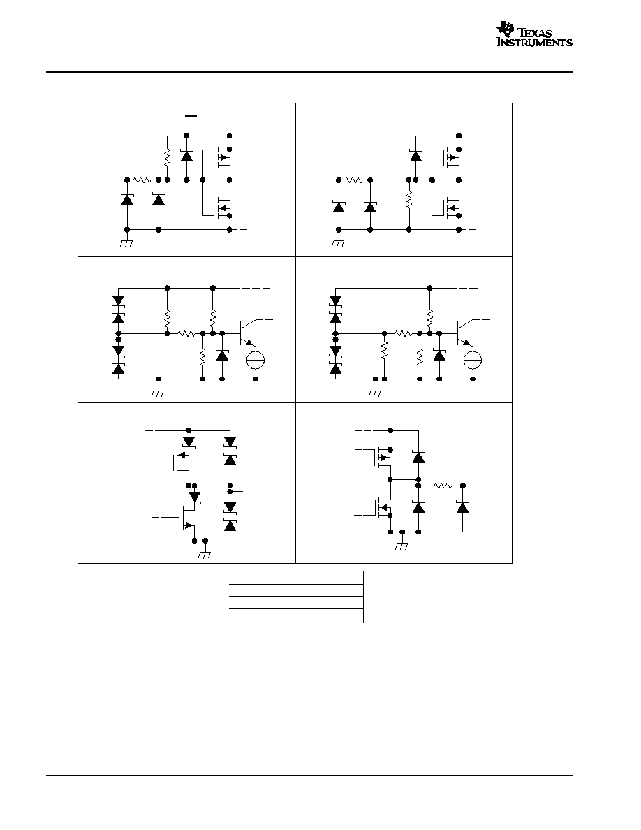
EQUIVALENT INPUT AND OUTPUT SCHEMATIC DIAGRAMS
9 V
1 k
100 k
Input
VCC
D and RE Inputs
9 V
1 k
100 k
Input
VCC
DE Input
16 V
16 V
100 k
R3
R1
R2
Input
A Input
16 V
16 V
100 k
R3
R1
R2
Input
B Input
16 V
16 V
VCC
A and B Outputs
9 V
VCC
R Output
5
Output
VCC
SN65HVD05
SN65HVD06
SN65HVD07
R1/R2
9 k
36 k
36 k
R3
45 k
180 k
180 k
VCC
Output
SN65HVD05, SN65HVD06, SN65HVD07
SN75HVD05, SN75HVD06, SN75HVD07
SLLS533B ≠ MAY 2002 ≠ REVISED MAY 2003
www.ti.com
13
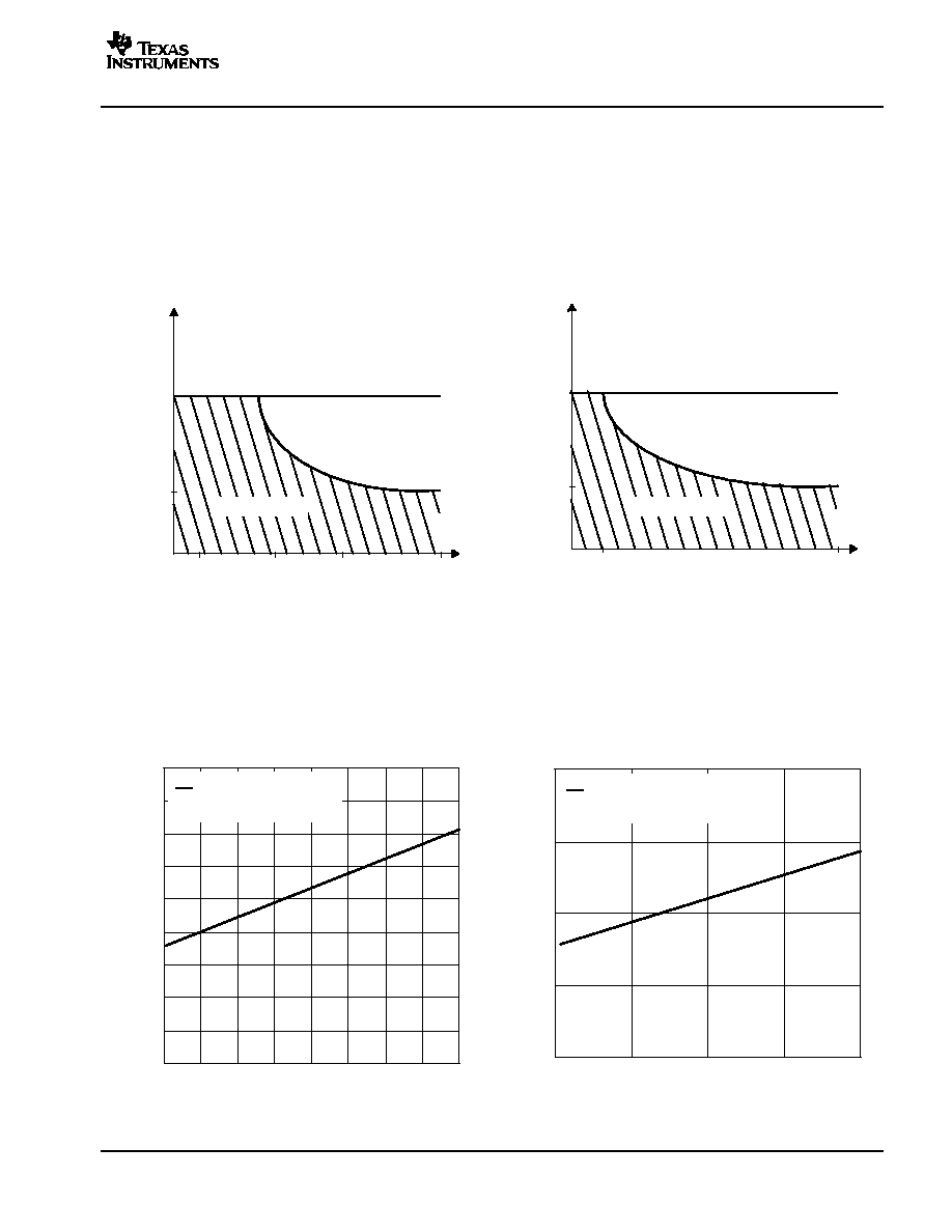
TYPICAL CHARACTERISTICS
HVD05
MAXIMUM RECOMMENDED STILL-AIR
OPERATING TEMPERATURE
vs
SIGNALING RATE
(D ≠ PACKAGE)
””””””””””””
””””””””””””
””””””””””””
””””””””””””
””””””””””””
””””””””””””
””””””””””””
””””””””””””
85
25
1
10
40
Maximum Recommended Still-Air
Operating T
emperature
≠
T
A
(
∞
C
Signaling Rate ≠ Mbps
)
High K Board
Low K Board
HVD06
MAXIMUM RECOMMENDED STILL-AIR
OPERATING TEMPERATURE
vs
SIGNALING RATE
(D ≠ PACKAGE)
”””””””””””””
”””””””””””””
”””””””””””””
”””””””””””””
”””””””””””””
”””””””””””””
”””””””””””””
85
25
1
10
Maximum Recommended Still-Air
Operating T
emperature
≠
T
A
Signaling Rate ≠ Mbps
(
∞
C)
High K Board
Low K Board
Figure 12
Figure 13
30
40
50
60
70
80
90
100
110
120
0
5
10
15
20
25
30
35
40
HVD05
RMS SUPPLY CURRENT
vs
SIGNALING RATE
I CC
≠
RMS Supply Current
≠
mA
TA = 25
∞
C
RE at VCC
DE at VCC
RL = 54
CL = 50 pF
VCC = 5 V
Signaling Rate ≠ Mbps
40
60
80
100
120
0
2.5
5
7.5
10
Signaling Rate ≠ Mbps
HVD06
RMS SUPPLY CURRENT
vs
SIGNALING RATE
I CC
≠
RMS Supply Current
≠
mA
TA = 25
∞
C
RE at VCC
DE at VCC
RL = 54
CL = 50 pF
VCC = 5 V
Figure 14
Figure 15

SN65HVD05, SN65HVD06, SN65HVD07
SN75HVD05, SN75HVD06, SN75HVD07
SLLS533B ≠ MAY 2002 ≠ REVISED MAY 2003
www.ti.com
14
40
50
60
70
80
90
100
110
100
400
700
1000
HVD07
RMS SUPPLY CURRENT
vs
SIGNALING RATE
I CC
≠
RMS Supply Current
≠
mA
TA = 25
∞
C
RE at VCC
DE at VCC
RL = 54
CL = 50 pF
VCC = 5 V
Signaling Rate ≠ kbps
≠7 ≠6≠5 ≠4≠3 ≠2≠1 0 1 2 3 4 5 6 7 8 9 10 11 12
≠
Bus Input Current
≠
BUS INPUT CURRENT
vs
BUS INPUT VOLTAGE
I I
A
µ
VI ≠ Bus Input Voltage ≠ V
TA = 25
∞
C
DE at 0 V
VCC = 5 V
≠200
≠150
≠100
≠50
0
50
100
150
200
250
HVD05
HVD06
HVD07
Figure 16
Figure 17
≠160
≠140
≠120
≠100
≠80
≠60
≠40
≠20
0
0
0.5
1
1.5
2
4.5
2.5
3
3.5
4
≠
Driver High-Level Output Current
≠
mA
DRIVER HIGH-LEVEL OUTPUT CURRENT
vs
HIGH-LEVEL OUTPUT VOLTAGE
I OH
VO ≠ High-Level Output Voltage ≠ V
5
TA = 25
∞
C
DE at VCC
D at VCC
VCC = 5 V
0
0.5
1
1.5
2
2.5
3
3.5
4
4.5
5
≠
Driver Low-Level Output Current
≠
mA
DRIVER LOW-LEVEL OUTPUT CURRENT
vs
LOW-LEVEL OUTPUT VOLTAGE
I OL
VO ≠ Low-Level Output Voltage ≠ V
0
20
40
60
80
100
120
140
160
TA = 25
∞
C
DE at VCC
D at 0 V
VCC = 5 V
Figure 18
Figure 19

SN65HVD05, SN65HVD06, SN65HVD07
SN75HVD05, SN75HVD06, SN75HVD07
SLLS533B ≠ MAY 2002 ≠ REVISED MAY 2003
www.ti.com
15
2
2.2
2.4
2.6
2.8
3
3.2
3.4
3.6
3.8
4
≠40
≠15
10
35
60
85
DIFFERENTIAL OUTPUT VOLTAGE
vs
FREE-AIR TEMPERATURE
V
OD
≠
Differential Output V
oltage
≠
V
TA ≠ Free-Air Temperature ≠
∞
C
DE at VCC
D at VCC
VCC = 5 V
RL = 54
0
0.6
1.2
1.8
2.4
3
3.6
4.2
4.8
5.4
0
10
20
30
40
50
60
70
I O
≠
Driver Output Current
≠
mA
DRIVER OUTPUT CURRENT
vs
SUPPLY VOLTAGE
VCC ≠ Supply Voltage ≠ V
TA = 25
∞
C
DE at VCC
D at VCC
RL = 54
Figure 20
Figure 21
0
0.5
1
1.5
2
2.5
3
3.5
4
4.5
5
0
20
40
60
80
100
120
≠
Differential Output V
oltage
≠
V
DIFFERENTIAL OUTPUT VOLTAGE
vs
DIFFERENTIAL OUTPUT CURRENT
V
O
IOD ≠ Differential Output Current ≠ mA
60
Load
Line
30
Load
Line
TA = 25
∞
C
DE at VCC
D at VCC
VCC = 5 V
Figure 22

SN65HVD05, SN65HVD06, SN65HVD07
SN75HVD05, SN75HVD06, SN75HVD07
SLLS533B ≠ MAY 2002 ≠ REVISED MAY 2003
www.ti.com
16
APPLICATION INFORMATION
RT
RT
Device
HVD05
HVD06
HVD07
Number of Devices on Bus
64
256
256
NOTE: The line should be terminated at both ends with its characteristic impedance (RT = ZO). Stub lengths off the main line should be kept as short
as possible.
Figure 23. Typical Application Circuit

MECHANICAL DATA
MPDI001A ≠ JANUARY 1995 ≠ REVISED JUNE 1999
POST OFFICE BOX 655303
∑
DALLAS, TEXAS 75265
P (R-PDIP-T8)
PLASTIC DUAL-IN-LINE
8
4
0.015 (0,38)
Gage Plane
0.325 (8,26)
0.300 (7,62)
0.010 (0,25) NOM
MAX
0.430 (10,92)
4040082/D 05/98
0.200 (5,08) MAX
0.125 (3,18) MIN
5
0.355 (9,02)
0.020 (0,51) MIN
0.070 (1,78) MAX
0.240 (6,10)
0.260 (6,60)
0.400 (10,60)
1
0.015 (0,38)
0.021 (0,53)
Seating Plane
M
0.010 (0,25)
0.100 (2,54)
NOTES: A. All linear dimensions are in inches (millimeters).
B. This drawing is subject to change without notice.
C. Falls within JEDEC MS-001
For the latest package information, go to http://www.ti.com/sc/docs/package/pkg_info.htm


IMPORTANT NOTICE
Texas Instruments Incorporated and its subsidiaries (TI) reserve the right to make corrections, modifications,
enhancements, improvements, and other changes to its products and services at any time and to discontinue
any product or service without notice. Customers should obtain the latest relevant information before placing
orders and should verify that such information is current and complete. All products are sold subject to TI's terms
and conditions of sale supplied at the time of order acknowledgment.
TI warrants performance of its hardware products to the specifications applicable at the time of sale in
accordance with TI's standard warranty. Testing and other quality control techniques are used to the extent TI
deems necessary to support this warranty. Except where mandated by government requirements, testing of all
parameters of each product is not necessarily performed.
TI assumes no liability for applications assistance or customer product design. Customers are responsible for
their products and applications using TI components. To minimize the risks associated with customer products
and applications, customers should provide adequate design and operating safeguards.
TI does not warrant or represent that any license, either express or implied, is granted under any TI patent right,
copyright, mask work right, or other TI intellectual property right relating to any combination, machine, or process
in which TI products or services are used. Information published by TI regarding third-party products or services
does not constitute a license from TI to use such products or services or a warranty or endorsement thereof.
Use of such information may require a license from a third party under the patents or other intellectual property
of the third party, or a license from TI under the patents or other intellectual property of TI.
Reproduction of information in TI data books or data sheets is permissible only if reproduction is without
alteration and is accompanied by all associated warranties, conditions, limitations, and notices. Reproduction
of this information with alteration is an unfair and deceptive business practice. TI is not responsible or liable for
such altered documentation.
Resale of TI products or services with statements different from or beyond the parameters stated by TI for that
product or service voids all express and any implied warranties for the associated TI product or service and
is an unfair and deceptive business practice. TI is not responsible or liable for any such statements.
Following are URLs where you can obtain information on other Texas Instruments products and application
solutions:
Products
Applications
Amplifiers
amplifier.ti.com
Audio
www.ti.com/audio
Data Converters
dataconverter.ti.com
Automotive
www.ti.com/automotive
DSP
dsp.ti.com
Broadband
www.ti.com/broadband
Interface
interface.ti.com
Digital Control
www.ti.com/digitalcontrol
Logic
logic.ti.com
Military
www.ti.com/military
Power Mgmt
power.ti.com
Optical Networking
www.ti.com/opticalnetwork
Microcontrollers
microcontroller.ti.com
Security
www.ti.com/security
Telephony
www.ti.com/telephony
Video & Imaging
www.ti.com/video
Wireless
www.ti.com/wireless
Mailing Address:
Texas Instruments
Post Office Box 655303 Dallas, Texas 75265
Copyright
2004, Texas Instruments Incorporated