SN54ABT16952, SN74ABT16952
16-BIT REGISTERED TRANSCEIVERS
WITH 3-STATE OUTPUTS
SCBS082C ≠ FEBRUARY 1991 ≠ REVISED JANUARY 1997
1
POST OFFICE BOX 655303
∑
DALLAS, TEXAS 75265
D
Members of the Texas Instruments
Widebus
TM
Family
D
State-of-the-Art
EPIC-
B
TM
BiCMOS Design
Significantly Reduces Power Dissipation
D
Latch-Up Performance Exceeds 500 mA Per
JEDEC Standard JESD-17
D
Typical V
OLP
(Output Ground Bounce) < 1 V
at V
CC
= 5 V, T
A
= 25
∞
C
D
Distributed V
CC
and GND Pin Configuration
Minimizes High-Speed Switching Noise
D
Flow-Through Architecture Optimizes PCB
Layout
D
High-Drive Outputs (≠32-mA I
OH
, 64-mA I
OL
)
D
Package Options Include Plastic 300-mil
Shrink Small-Outline (DL) and Thin Shrink
Small-Outline (DGG) Packages and 380-mil
Fine-Pitch Ceramic Flat (WD) Package
Using 25-mil Center-to-Center Spacings
description
The 'ABT16952 are 16-bit registered transceivers
that contain two sets of D-type flip-flops for
temporary storage of data flowing in either
direction. The 'ABT16952 can be used as two 8-bit
transceivers or one 16-bit transceiver. Data on the
A or B bus is stored in the registers on the
low-to-high transition of the clock (CLKAB or
CLKBA) input provided that the clock-enable
(CLKENAB or CLKENBA) input is low. Taking the
output-enable (OEAB or OEBA) input low
accesses the data on either port.
To ensure the high-impedance state during power up or power down, OE should be tied to V
CC
through a pullup
resistor; the minimum value of the resistor is determined by the current-sinking capability of the driver.
The SN54ABT16952 is characterized for operation over the full military temperature range of ≠55
∞
C to 125
∞
C.
The SN74ABT16952 is characterized for operation from ≠40
∞
C to 85
∞
C.
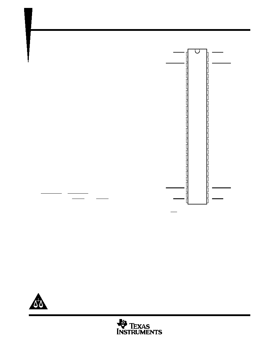
SN54ABT16952 . . . WD PACKAGE
SN74ABT16952 . . . DGG OR DL PACKAGE
(TOP VIEW)
1
2
3
4
5
6
7
8
9
10
11
12
13
14
15
16
17
18
19
20
21
22
23
24
25
26
27
28
56
55
54
53
52
51
50
49
48
47
46
45
44
43
42
41
40
39
38
37
36
35
34
33
32
31
30
29
1OEAB
1CLKAB
1CLKENAB
GND
1A1
1A2
V
CC
1A3
1A4
1A5
GND
1A6
1A7
1A8
2A1
2A2
2A3
GND
2A4
2A5
2A6
V
CC
2A7
2A8
GND
2CLKENAB
2CLKAB
2OEAB
1OEBA
1CLKBA
1CLKENBA
GND
1B1
1B2
V
CC
1B3
1B4
1B5
GND
1B6
1B7
1B8
2B1
2B2
2B3
GND
2B4
2B5
2B6
V
CC
2B7
2B8
GND
2CLKENBA
2CLKBA
2OEBA
Copyright
©
1997, Texas Instruments Incorporated
UNLESS OTHERWISE NOTED this document contains PRODUCTION
DATA information current as of publication date. Products conform to
specifications per the terms of Texas Instruments standard warranty.
Production processing does not necessarily include testing of all
parameters.
Widebus and EPIC-
B are trademarks of Texas Instruments Incorporated.
Please be aware that an important notice concerning availability, standard warranty, and use in critical applications of
Texas Instruments semiconductor products and disclaimers thereto appears at the end of this data sheet.
SN54ABT16952, SN74ABT16952
16-BIT REGISTERED TRANSCEIVERS
WITH 3-STATE OUTPUTS
SCBS082C ≠ FEBRUARY 1991 ≠ REVISED JANUARY 1997
2
POST OFFICE BOX 655303
∑
DALLAS, TEXAS 75265
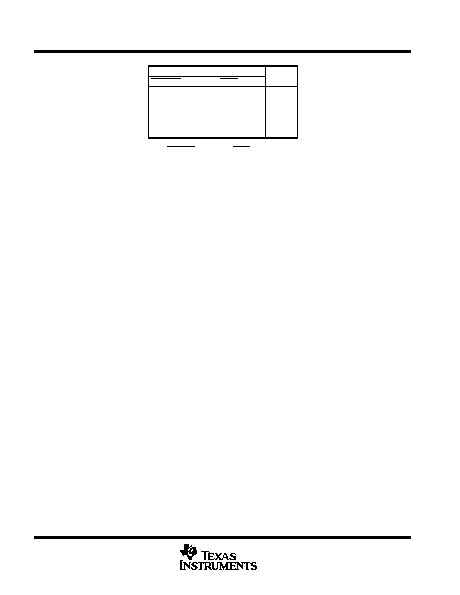
FUNCTION TABLE
INPUTS
OUTPUT
CLKENAB
CLKAB
OEAB
A
B
H
X
L
X
B0
X
L
L
X
B0
L
L
L
L
L
L
H
H
X
X
H
X
Z
A-to-B data flow is shown; B-to-A data flow is similar, but
uses CLKENBA, CLKBA, and OEBA.
Level of B before the indicated steady-state input
conditions were established
SN54ABT16952, SN74ABT16952
16-BIT REGISTERED TRANSCEIVERS
WITH 3-STATE OUTPUTS
SCBS082C ≠ FEBRUARY 1991 ≠ REVISED JANUARY 1997
3
POST OFFICE BOX 655303
∑
DALLAS, TEXAS 75265
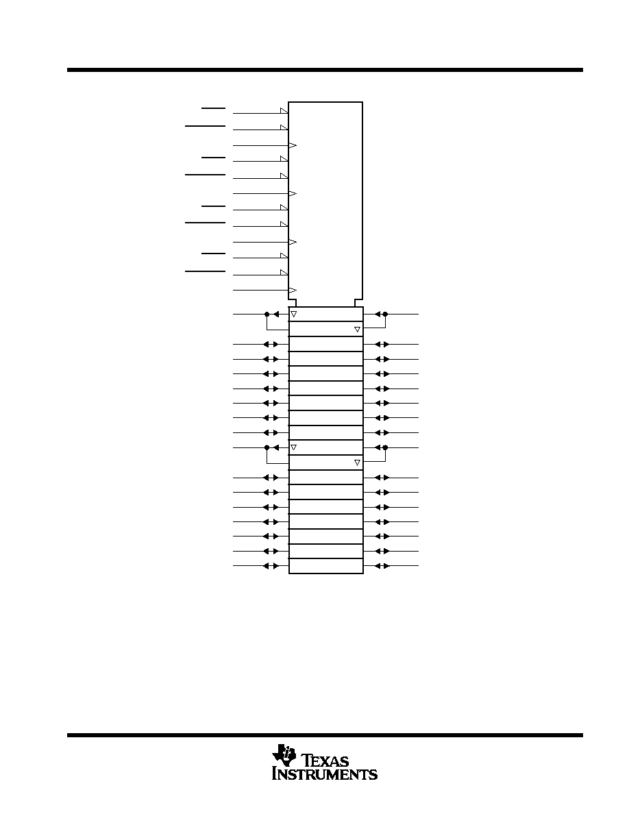
logic symbol
1OEBA
1CLKENBA
1OEAB
1CLKENAB
2OEBA
2CLKENBA
2OEAB
2CLKENAB
G8
26
27
2CLKAB
8C12
1A1
5
6D
1A2
6
1A3
8
1A4
9
1A5
10
1A6
12
1A7
13
1A8
14
1B1
52
5D
1B6
45
1B7
44
1B8
43
1B2
51
1B3
49
1B4
48
1B5
47
EN10
28
G7
31
30
2CLKBA
7C11
EN9
29
G2
3
2
1CLKAB
2C6
EN4
1
G1
54
55
1CLKBA
1C5
EN3
56
2A1
15
12D
2A2
16
2A3
17
2A4
19
2A5
20
2A6
21
2A7
23
2A8
24
2B1
42
11D
2B6
36
2B7
34
2B8
33
2B2
41
2B3
40
2B4
38
2B5
37
This symbol is in accordance with ANSI/IEEE Std 91-1984 and IEC Publication 617-12.
4
10
9
3
SN54ABT16952, SN74ABT16952
16-BIT REGISTERED TRANSCEIVERS
WITH 3-STATE OUTPUTS
SCBS082C ≠ FEBRUARY 1991 ≠ REVISED JANUARY 1997
4
POST OFFICE BOX 655303
∑
DALLAS, TEXAS 75265
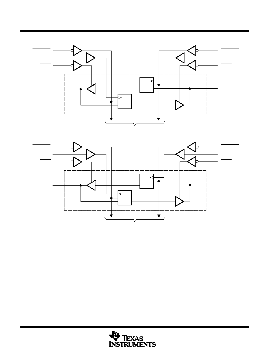
logic diagram (positive logic)
One of Eight
Channels
1A1
One of Eight
Channels
To Seven Other Channels
1CLKAB
1CLKBA
1OEBA
1OEAB
1B1
1CLKENAB
1CLKENBA
To Seven Other Channels
2CLKAB
2CLKBA
2OEBA
2OEAB
2A1
2B1
2CLKENAB
2CLKENBA
3
2
56
5
26
27
29
15
C1
CE
1D
54
55
1
52
31
30
28
42
C1
CE
1D
C1
CE
1D
C1
CE
1D

SN54ABT16952, SN74ABT16952
16-BIT REGISTERED TRANSCEIVERS
WITH 3-STATE OUTPUTS
SCBS082C ≠ FEBRUARY 1991 ≠ REVISED JANUARY 1997
5
POST OFFICE BOX 655303
∑
DALLAS, TEXAS 75265
absolute maximum ratings over operating free-air temperature range (unless otherwise noted)
Supply voltage range, V
CC
≠0.5 V to 7 V
. . . . . . . . . . . . . . . . . . . . . . . . . . . . . . . . . . . . . . . . . . . . . . . . . . . . . . . . . .
Input voltage range, V
I
(except I/O ports) (see Note 1)
≠0.5 V to 7 V
. . . . . . . . . . . . . . . . . . . . . . . . . . . . . . . . . .
Voltage range applied to any output in the high or power-off state, V
O
≠0.5 V to 5.5 V
. . . . . . . . . . . . . . . . . . . .
Current into any output in the low state, I
O
: SN54ABT16952 96
mA
. . . . . . . . . . . . . . . . . . . . . . . . . . . . . . . . . .
SN74ABT16952 128
mA
. . . . . . . . . . . . . . . . . . . . . . . . . . . . . . . . .
Input clamp current, I
IK
(V
I
< 0)
≠18 mA
. . . . . . . . . . . . . . . . . . . . . . . . . . . . . . . . . . . . . . . . . . . . . . . . . . . . . . . . . . . .
Output clamp current, I
OK
(V
O
< 0)
≠50 mA
. . . . . . . . . . . . . . . . . . . . . . . . . . . . . . . . . . . . . . . . . . . . . . . . . . . . . . . .
Package thermal impedance,
JA
(see Note 2): DGG package
81
∞
C/W
. . . . . . . . . . . . . . . . . . . . . . . . . . . . . . . .
DL package
74
∞
C/W
. . . . . . . . . . . . . . . . . . . . . . . . . . . . . . . . . .
Storage temperature range, T
stg
≠65
∞
C to 150
∞
C
. . . . . . . . . . . . . . . . . . . . . . . . . . . . . . . . . . . . . . . . . . . . . . . . . . . .
Stresses beyond those listed under "absolute maximum ratings" may cause permanent damage to the device. These are stress ratings only, and
functional operation of the device at these or any other conditions beyond those indicated under "recommended operating conditions" is not
implied. Exposure to absolute-maximum-rated conditions for extended periods may affect device reliability.
NOTES:
1. The input and output negative-voltage ratings may be exceeded if the input and output clamp-current ratings are observed.
2. The package thermal impedance is calculated in accordance with EIA/JEDEC Std JESD51.
recommended operating conditions (see Note 3)
SN54ABT16952
SN74ABT16952
UNIT
MIN
MAX
MIN
MAX
UNIT
VCC
Supply voltage
4.5
5.5
4.5
5.5
V
VIH
High-level input voltage
2
2
V
VIL
Low-level input voltage
0.8
0.8
V
VI
Input voltage
0
VCC
0
VCC
V
IOH
High-level output current
≠24
≠32
mA
IOL
Low-level output current
48
64
mA
t/
v
Input transition rise or fall rate
Outputs enabled
10
10
ns/V
TA
Operating free-air temperature
≠55
125
≠40
85
∞
C
NOTE 3: Unused pins (input or I/O) must be held high or low to prevent them from floating.
PRODUCT PREVIEW information concerns products in the formative or
design phase of development. Characteristic data and other
specifications are design goals. Texas Instruments reserves the right to
change or discontinue these products without notice.
SN54ABT16952, SN74ABT16952
16-BIT REGISTERED TRANSCEIVERS
WITH 3-STATE OUTPUTS
SCBS082C ≠ FEBRUARY 1991 ≠ REVISED JANUARY 1997
6
POST OFFICE BOX 655303
∑
DALLAS, TEXAS 75265
electrical characteristics over recommended operating free-air temperature range (unless
otherwise noted)
PARAMETER
TEST CONDITIONS
TA = 25
∞
C
SN54ABT16952
SN74ABT16952
UNIT
PARAMETER
TEST CONDITIONS
MIN
TYP
MAX
MIN
MAX
MIN
MAX
UNIT
VIK
VCC = 4.5 V,
II = ≠18 mA
≠1.2
≠1.2
≠1.2
V
VCC = 4.5 V,
IOH = ≠3 mA
2.5
2.5
2.5
VOH
VCC = 5 V,
IOH = ≠3 mA
3
3
3
V
VOH
VCC = 4 5 V
IOH = ≠24 mA
2
2
V
VCC = 4.5 V
IOH = ≠32 mA
2*
2
VOL
VCC = 4 5 V
IOL = 48 mA
0.55
0.55
V
VOL
VCC = 4.5 V
IOL = 64 mA
0.55*
0.55
V
Vhys
100
mV
II
Control inputs
VCC = 5 5 V
VI = VCC or GND
±
1
±
1
±
1
µ
A
II
A or B ports
VCC = 5.5 V,
VI = VCC or GND
±
100
±
100
±
100
µ
A
IOZH
VCC = 5.5 V,
VO = 2.7 V
50
50
50
µ
A
IOZL
VCC = 5.5 V,
VO = 0.5 V
≠50
≠50
≠50
µ
A
Ioff
VCC = 0,
VI or VO
4.5 V
±
100
±
100
µ
A
ICEX
VCC = 5.5 V,
VO = 5.5 V
Outputs high
50
50
50
µ
A
IOß
VCC = 5.5 V,
VO = 2.5 V
≠50
≠100
≠200
≠50
≠200
≠50
≠200
mA
VCC = 5.5 V,
Outputs high
2
2
2
ICC
A or B ports
VCC = 5.5 V,
IO = 0,
Outputs low
35
35
35
mA
VI = VCC or GND Outputs disabled
2
2
2
ICC∂
VCC = 5.5 V, One input at 3.4 V,
Other inputs at VCC or GND
0.5
0.5
0.5
mA
Ci
Control inputs
VI = 2.5 V or 0.5 V
3
pF
Cio
A or B ports
VO = 2.5 V or 0.5 V
8.5
pF
* On products compliant to MIL-PRF-38535, this parameter does not apply.
All typical values are at VCC = 5 V.
The parameters IOZH and IOZL include the input leakage current.
ß Not more than one output should be tested at a time, and the duration of the test should not exceed one second.
∂ This is the increase in supply current for each input that is at the specified TTL voltage level rather than VCC or GND.
PRODUCT PREVIEW information concerns products in the formative or
design phase of development. Characteristic data and other
specifications are design goals. Texas Instruments reserves the right to
change or discontinue these products without notice.

SN54ABT16952, SN74ABT16952
16-BIT REGISTERED TRANSCEIVERS
WITH 3-STATE OUTPUTS
SCBS082C ≠ FEBRUARY 1991 ≠ REVISED JANUARY 1997
7
POST OFFICE BOX 655303
∑
DALLAS, TEXAS 75265
timing requirements over recommended ranges of supply voltage and operating free-air
temperature (unless otherwise noted) (see Figure 1)
VCC = 5 V,
TA = 25
∞
C
SN54ABT16952
SN74ABT16952
UNIT
MIN
MAX
MIN
MAX
MIN
MAX
fclock
Clock frequency
0
150
0
150
0
150
MHz
tw
Pulse duration, CLKAB or CLKBA high or low
3.3
3.3
3.3
ns
t
Setup time,
A or B
3.5
3.5
3.5
ns
tsu
,
before CLKAB
or CLKBA
CLKENAB or CLKENBA
3
3
3
ns
th
Hold time,
A or B
1
1
1
ns
th
,
after CLKAB
or CLKBA
CLKENAB or CLKENBA
1
1
1
ns
This parameter is warranted, but not production tested.
switching characteristics over recommended ranges of supply voltage and operating free-air
temperature, C
L
= 50 pF (unless otherwise noted) (see Figure 1)
PARAMETER
FROM
(INPUT)
TO
(OUTPUT)
VCC = 5 V,
TA = 25
∞
C
SN54ABT16952
SN74ABT16952
UNIT
(INPUT)
(OUTPUT)
MIN
TYP
MAX
MIN
MAX
MIN
MAX
fmax
150
150
150
MHz
tPLH
CLK
A or B
1
2.6
3.9
1
4.4
1
4.3
ns
tPHL
CLK
A or B
1
2.6
4.2
1
4.6
1
4.5
ns
tPZH
OE
A or B
1
2.5
3.8
1
4.7
1
4.6
ns
tPZL
OE
A or B
1
2.8
5.1
1
6.1
1
6
ns
tPHZ
OE
A or B
1.7
3.4
4.7
1.7
6.1
1.7
5.5
ns
tPLZ
OE
A or B
1.3
3
3.9
1.3
4.8
1.3
4.2
ns
PRODUCT PREVIEW information concerns products in the formative or
design phase of development. Characteristic data and other
specifications are design goals. Texas Instruments reserves the right to
change or discontinue these products without notice.
SN54ABT16952, SN74ABT16952
16-BIT REGISTERED TRANSCEIVERS
WITH 3-STATE OUTPUTS
SCBS082C ≠ FEBRUARY 1991 ≠ REVISED JANUARY 1997
8
POST OFFICE BOX 655303
∑
DALLAS, TEXAS 75265
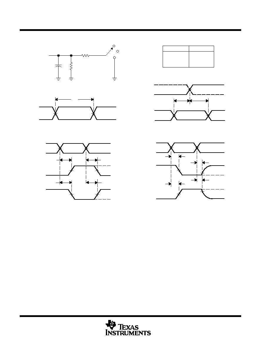
PARAMETER MEASUREMENT INFORMATION
1.5 V
th
tsu
From Output
Under Test
CL = 50 pF
(see Note A)
LOAD CIRCUIT
S1
7 V
Open
GND
500
500
Data Input
Timing Input
1.5 V
3 V
0 V
1.5 V
1.5 V
3 V
0 V
3 V
0 V
1.5 V
tw
Input
VOLTAGE WAVEFORMS
SETUP AND HOLD TIMES
VOLTAGE WAVEFORMS
PROPAGATION DELAY TIMES
INVERTING AND NONINVERTING OUTPUTS
VOLTAGE WAVEFORMS
PULSE DURATION
tPLH
tPHL
tPHL
tPLH
VOH
VOH
VOL
VOL
1.5 V
1.5 V
3 V
0 V
1.5 V
1.5 V
Input
1.5 V
Output
Control
Output
Waveform 1
S1 at 7 V
(see Note B)
Output
Waveform 2
S1 at Open
(see Note B)
VOL
VOH
tPZL
tPZH
tPLZ
tPHZ
1.5 V
1.5 V
3.5 V
0 V
1.5 V
VOL + 0.3 V
1.5 V
VOH ≠ 0.3 V
0 V
3 V
VOLTAGE WAVEFORMS
ENABLE AND DISABLE TIMES
LOW- AND HIGH-LEVEL ENABLING
Output
Output
tPLH/tPHL
tPLZ/tPZL
tPHZ/tPZH
Open
7 V
Open
TEST
S1
Output
Control
NOTES: A. CL includes probe and jig capacitance.
B. Waveform 1 is for an output with internal conditions such that the output is low except when disabled by the output control.
Waveform 2 is for an output with internal conditions such that the output is high except when disabled by the output control.
C. All input pulses are supplied by generators having the following characteristics: PRR
10 MHz, ZO = 50
, tr
2.5 ns, tf
2.5 ns.
D. The outputs are measured one at a time with one transition per measurement.
1.5 V
Figure 1. Load Circuit and Voltage Waveforms
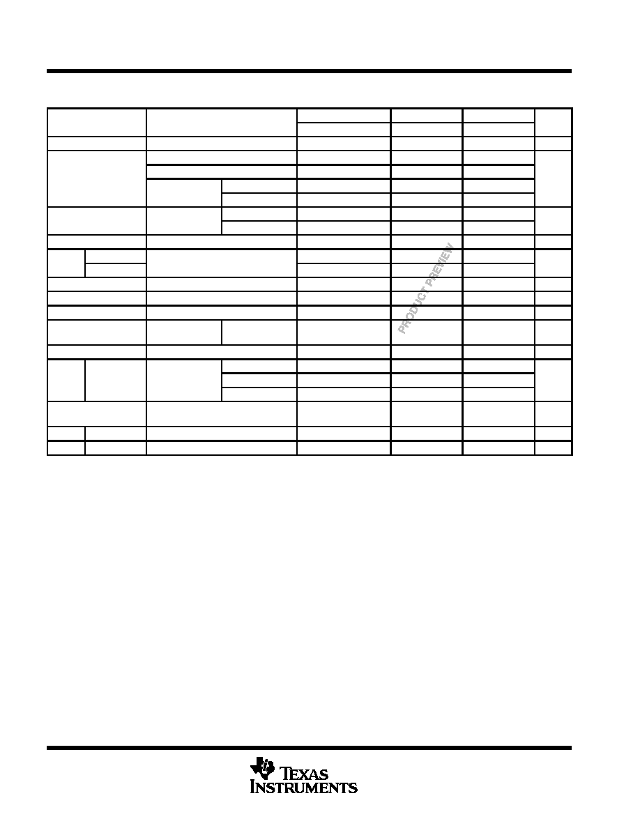
PACKAGING INFORMATION
Orderable Device
Status
(1)
Package
Type
Package
Drawing
Pins Package
Qty
Eco Plan
(2)
Lead/Ball Finish
MSL Peak Temp
(3)
74ABT16952DGGRE4
ACTIVE
TSSOP
DGG
56
2000 Green (RoHS &
no Sb/Br)
CU NIPDAU
Level-1-260C-UNLIM
SN74ABT16952DGGR
ACTIVE
TSSOP
DGG
56
2000 Green (RoHS &
no Sb/Br)
CU NIPDAU
Level-1-260C-UNLIM
SN74ABT16952DL
ACTIVE
SSOP
DL
56
20
Green (RoHS &
no Sb/Br)
CU NIPDAU
Level-1-260C-UNLIM
SN74ABT16952DLR
ACTIVE
SSOP
DL
56
1000 Green (RoHS &
no Sb/Br)
CU NIPDAU
Level-1-260C-UNLIM
SN74ABT16952DLRG4
ACTIVE
SSOP
DL
56
1000 Green (RoHS &
no Sb/Br)
CU NIPDAU
Level-1-260C-UNLIM
(1)
The marketing status values are defined as follows:
ACTIVE: Product device recommended for new designs.
LIFEBUY: TI has announced that the device will be discontinued, and a lifetime-buy period is in effect.
NRND: Not recommended for new designs. Device is in production to support existing customers, but TI does not recommend using this part in
a new design.
PREVIEW: Device has been announced but is not in production. Samples may or may not be available.
OBSOLETE: TI has discontinued the production of the device.
(2)
Eco
Plan
-
The
planned
eco-friendly
classification:
Pb-Free
(RoHS)
or
Green
(RoHS
&
no
Sb/Br)
-
please
check
http://www.ti.com/productcontent
for the latest availability information and additional product content details.
TBD: The Pb-Free/Green conversion plan has not been defined.
Pb-Free (RoHS): TI's terms "Lead-Free" or "Pb-Free" mean semiconductor products that are compatible with the current RoHS requirements
for all 6 substances, including the requirement that lead not exceed 0.1% by weight in homogeneous materials. Where designed to be soldered
at high temperatures, TI Pb-Free products are suitable for use in specified lead-free processes.
Green (RoHS & no Sb/Br): TI defines "Green" to mean Pb-Free (RoHS compatible), and free of Bromine (Br) and Antimony (Sb) based flame
retardants (Br or Sb do not exceed 0.1% by weight in homogeneous material)
(3)
MSL, Peak Temp. -- The Moisture Sensitivity Level rating according to the JEDEC industry standard classifications, and peak solder
temperature.
Important Information and Disclaimer:The information provided on this page represents TI's knowledge and belief as of the date that it is
provided. TI bases its knowledge and belief on information provided by third parties, and makes no representation or warranty as to the
accuracy of such information. Efforts are underway to better integrate information from third parties. TI has taken and continues to take
reasonable steps to provide representative and accurate information but may not have conducted destructive testing or chemical analysis on
incoming materials and chemicals. TI and TI suppliers consider certain information to be proprietary, and thus CAS numbers and other limited
information may not be available for release.
In no event shall TI's liability arising out of such information exceed the total purchase price of the TI part(s) at issue in this document sold by TI
to Customer on an annual basis.
PACKAGE OPTION ADDENDUM
www.ti.com
5-Sep-2005
Addendum-Page 1

IMPORTANT NOTICE
Texas Instruments Incorporated and its subsidiaries (TI) reserve the right to make corrections, modifications,
enhancements, improvements, and other changes to its products and services at any time and to discontinue
any product or service without notice. Customers should obtain the latest relevant information before placing
orders and should verify that such information is current and complete. All products are sold subject to TI's terms
and conditions of sale supplied at the time of order acknowledgment.
TI warrants performance of its hardware products to the specifications applicable at the time of sale in
accordance with TI's standard warranty. Testing and other quality control techniques are used to the extent TI
deems necessary to support this warranty. Except where mandated by government requirements, testing of all
parameters of each product is not necessarily performed.
TI assumes no liability for applications assistance or customer product design. Customers are responsible for
their products and applications using TI components. To minimize the risks associated with customer products
and applications, customers should provide adequate design and operating safeguards.
TI does not warrant or represent that any license, either express or implied, is granted under any TI patent right,
copyright, mask work right, or other TI intellectual property right relating to any combination, machine, or process
in which TI products or services are used. Information published by TI regarding third-party products or services
does not constitute a license from TI to use such products or services or a warranty or endorsement thereof.
Use of such information may require a license from a third party under the patents or other intellectual property
of the third party, or a license from TI under the patents or other intellectual property of TI.
Reproduction of information in TI data books or data sheets is permissible only if reproduction is without
alteration and is accompanied by all associated warranties, conditions, limitations, and notices. Reproduction
of this information with alteration is an unfair and deceptive business practice. TI is not responsible or liable for
such altered documentation.
Resale of TI products or services with statements different from or beyond the parameters stated by TI for that
product or service voids all express and any implied warranties for the associated TI product or service and
is an unfair and deceptive business practice. TI is not responsible or liable for any such statements.
Following are URLs where you can obtain information on other Texas Instruments products and application
solutions:
Products
Applications
Amplifiers
amplifier.ti.com
Audio
www.ti.com/audio
Data Converters
dataconverter.ti.com
Automotive
www.ti.com/automotive
DSP
dsp.ti.com
Broadband
www.ti.com/broadband
Interface
interface.ti.com
Digital Control
www.ti.com/digitalcontrol
Logic
logic.ti.com
Military
www.ti.com/military
Power Mgmt
power.ti.com
Optical Networking
www.ti.com/opticalnetwork
Microcontrollers
microcontroller.ti.com
Security
www.ti.com/security
Telephony
www.ti.com/telephony
Video & Imaging
www.ti.com/video
Wireless
www.ti.com/wireless
Mailing Address:
Texas Instruments
Post Office Box 655303 Dallas, Texas 75265
Copyright
2005, Texas Instruments Incorporated