74ACT11867
SYNCHRONOUS 8-BIT UP/DOWN BINARY COUNTER
WITH ASYNCHRONOUS CLEAR
SCAS178A ≠ DECEMBER 1991 ≠ REVISED FEBRUARY 1998
1
POST OFFICE BOX 655303
∑
DALLAS, TEXAS 75265
D
Inputs Are TTL-Voltage Compatible
D
Asynchronous Clear
D
Fully Independent Clock Circuit Simplifies
Use
D
Flow-Through Architecture Optimizes PCB
Layout
D
Center-Pin V
CC
and GND Configurations
Minimize High-Speed Switching Noise
D
EPIC
TM
(Enhanced-Performance Implanted
CMOS) 1-
µ
m Process
D
500-mA Typical Latch-Up Immunity at
125
∞
C
description
The 74ACT11867 is a synchronous presettable
binary counter featuring an internal carry
look-ahead for cascading in high-speed counting
applications. Synchronous operation is provided
by having all flip-flops clocked simultaneously so
that the outputs change coincident with each other when so instructed by the count-enable inputs and internal
gating. This mode of operation helps eliminate the output counting spikes that are normally associated with
asynchronous (ripple-clock) counters. A buffered clock (CLK) input triggers the eight flip-flops on the rising
(positive-going) edge of the clock waveform.
The counters are fully programmable; that is, the outputs can each be preset to either logic level. The load-mode
circuitry allows parallel loading of the cascaded counters. As loading is synchronous, selecting the load mode
disables the counter and causes the outputs to agree with the data inputs after the next clock rising edge.
The carry look-ahead circuitry is provided for cascading counters for n-bit synchronous applications without
additional gating. This is done with two count-enable inputs and a carry output. Both count-enable (ENP and
ENT) inputs must be low to count. The direction of the count is determined by the levels of the select (S0 and
S1) inputs (see the function table). Input ENT is fed forward to enable the ripple-carry (RCO) output. RCO then
produces a low-level pulse while the count is zero (all outputs low) when counting down or 255 during counting
up (all outputs high). This low-level overflow carry pulse can be used to enable successive cascaded stages.
Transitions at ENP and ENT are allowed regardless of the level of the clock input.
These counters feature a fully independent clock circuit. Whenever ENP and/or ENT is taken high, RCO either
goes high or remains high. The function of the counter (whether enabled, disabled, loading, or counting) is
dictated solely by the conditions meeting the stable setup and hold times.
The 74ACT11867 is characterized for operation from ≠40
∞
C to 85
∞
C.
Copyright
©
1998, Texas Instruments Incorporated
PRODUCTION DATA information is current as of publication date.
Products conform to specifications per the terms of Texas Instruments
standard warranty. Production processing does not necessarily include
testing of all parameters.
EPIC is a trademark of Texas Instruments Incorporated.
Please be aware that an important notice concerning availability, standard warranty, and use in critical applications of
Texas Instruments semiconductor products and disclaimers thereto appears at the end of this data sheet.
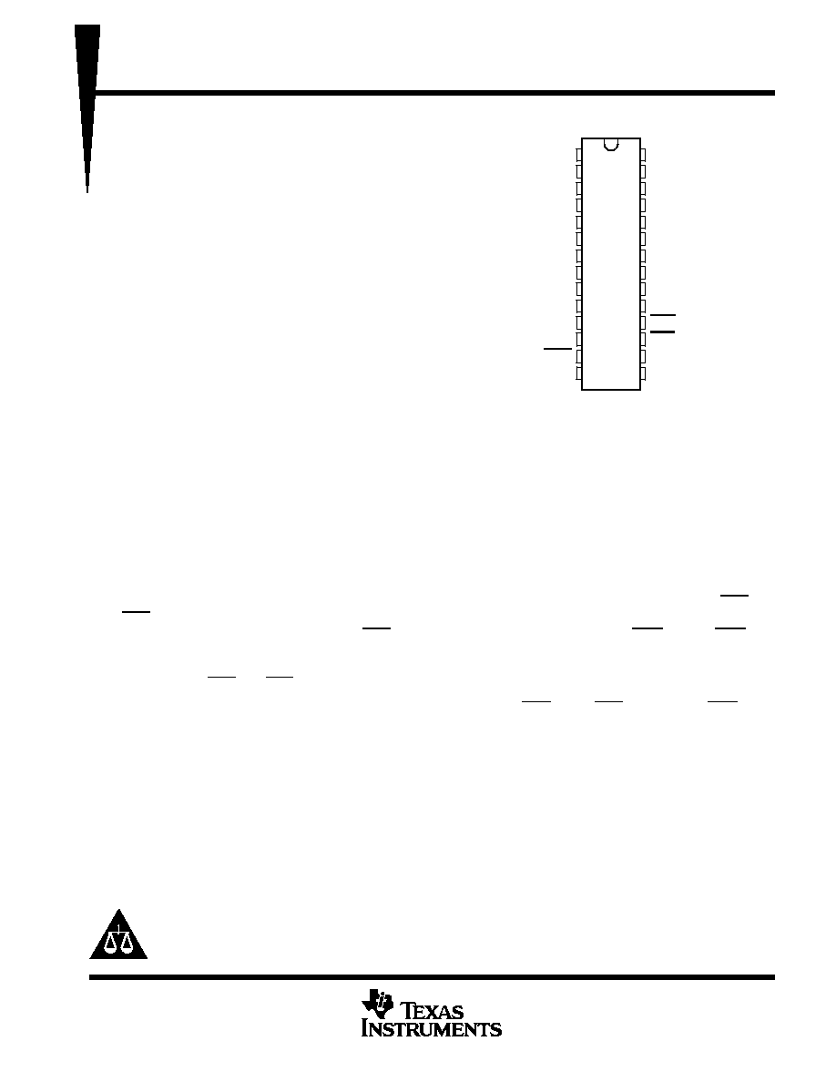
Q
A
Q
B
Q
C
Q
D
Q
E
GND
GND
GND
GND
Q
F
Q
G
Q
H
RCO
CLK
DW PACKAGE
(TOP VIEW)
1
2
3
4
5
6
7
8
9
10
11
12
13
14
28
27
26
25
24
23
22
21
20
19
18
17
16
15
A
B
C
D
E
F
V
CC
V
CC
G
H
ENP
ENT
S0
S1

74ACT11867
SYNCHRONOUS 8-BIT UP/DOWN BINARY COUNTER
WITH ASYNCHRONOUS CLEAR
SCAS178A ≠ DECEMBER 1991 ≠ REVISED FEBRUARY 1998
2
POST OFFICE BOX 655303
∑
DALLAS, TEXAS 75265
MODE FUNCTION TABLE
S1
S0
FUNCTION
L
L
Clear
L
H
Count down
H
L
Load
H
H
Count up
logic symbol
2,6D
28
A
27
B
26
C
25
D
1
2
3
4
ENT
CTRDIV256
0
16
S0
G4
17
C6/1,4,5≠/3,4,5+
13
1,4,5CT = 0
3,4,5CT = 255
24
E
23
F
20
G
19
H
5
10
11
12
1
15
S1
G5
18
14
CLK
ENP
RCO
0
3
M
0R
0
QA
QB
QC
QD
QE
QF
QG
QH
This symbol is in accordance with ANSI/IEEE Std 91-1984 and IEC Publication 617-12.
74ACT11867
SYNCHRONOUS 8-BIT UP/DOWN BINARY COUNTER
WITH ASYNCHRONOUS CLEAR
SCAS178A ≠ DECEMBER 1991 ≠ REVISED FEBRUARY 1998
3
POST OFFICE BOX 655303
∑
DALLAS, TEXAS 75265
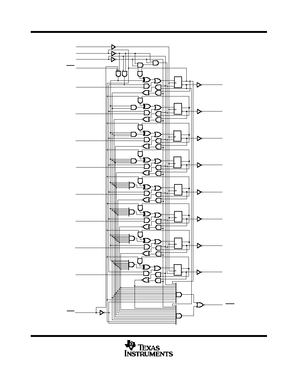
logic diagram (positive logic)
RCO
ENT
ENP
1D
C1
R
CLK
S0
S1
A
B
C
D
E
F
G
H
17
19
20
23
24
25
26
27
28
18
15
16
14
1
2
3
4
5
10
11
12
13
Q
Q
Q
Q
Q
Q
Q
Q
H
G
F
E
D
C
B
A
1D
C1
R
1D
C1
R
1D
C1
R
1D
C1
R
1D
C1
R
1D
C1
R
1D
C1
R
74ACT11867
SYNCHRONOUS 8-BIT UP/DOWN BINARY COUNTER
WITH ASYNCHRONOUS CLEAR
SCAS178A ≠ DECEMBER 1991 ≠ REVISED FEBRUARY 1998
4
POST OFFICE BOX 655303
∑
DALLAS, TEXAS 75265
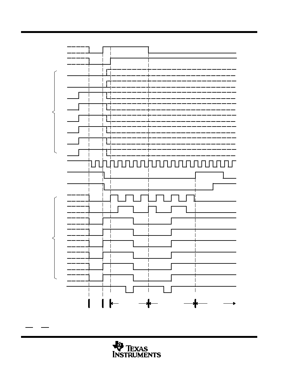
output sequence
Count Up
C
Async
Clear
Inhibit
0
1
2
D
E
F
CLK
ENP
ENT
QA
QB
QC
QD
RCO
Data
Inputs
Outputs
QE
QF
QG
QH
Count Down
1
0
255 254 253 252
255
254
253
G
H
B
A
S1
S0
Preset
Outputs
to 252
ENT and ENP must both be low for counting to occur.

74ACT11867
SYNCHRONOUS 8-BIT UP/DOWN BINARY COUNTER
WITH ASYNCHRONOUS CLEAR
SCAS178A ≠ DECEMBER 1991 ≠ REVISED FEBRUARY 1998
5
POST OFFICE BOX 655303
∑
DALLAS, TEXAS 75265
absolute maximum ratings over operating free-air temperature range (unless otherwise noted)
Supply voltage range, V
CC
≠0.5 V to 7 V
. . . . . . . . . . . . . . . . . . . . . . . . . . . . . . . . . . . . . . . . . . . . . . . . . . . . . . . . . .
Input voltage range, V
I
(see Note 1)
≠0.5 V to V
CC
+ 0.5 V
. . . . . . . . . . . . . . . . . . . . . . . . . . . . . . . . . . . . . . . . . . .
Output voltage range, V
O
(see Note 1)
≠0.5 V to V
CC
+ 0.5 V
. . . . . . . . . . . . . . . . . . . . . . . . . . . . . . . . . . . . . . . .
Input clamp current, I
IK
(V
I
< 0 or V
I
> V
CC
)
±
20 mA
. . . . . . . . . . . . . . . . . . . . . . . . . . . . . . . . . . . . . . . . . . . . . . . .
Output clamp current, I
OK
(V
O
< 0 or V
O
> V
CC
)
±
50 mA
. . . . . . . . . . . . . . . . . . . . . . . . . . . . . . . . . . . . . . . . . . . .
Continuous output current, I
O
(V
O
= 0 to V
CC
)
±
50 mA
. . . . . . . . . . . . . . . . . . . . . . . . . . . . . . . . . . . . . . . . . . . . . .
Continuous current through V
CC
or GND
±
225 mA
. . . . . . . . . . . . . . . . . . . . . . . . . . . . . . . . . . . . . . . . . . . . . . . . . .
Package thermal impedance,
JA
(see Note 2): DW package
78
∞
C/W
. . . . . . . . . . . . . . . . . . . . . . . . . . . . . . . . .
Storage temperature range, T
stg
≠65
∞
C to 150
∞
C
. . . . . . . . . . . . . . . . . . . . . . . . . . . . . . . . . . . . . . . . . . . . . . . . . .
Stresses beyond those listed under "absolute maximum ratings" may cause permanent damage to the device. These are stress ratings only, and
functional operation of the device at these or any other conditions beyond those indicated under "recommended operating conditions" is not
implied. Exposure to absolute-maximum-rated conditions for extended periods may affect device reliability.
NOTES:
1. The input and output voltage ratings may be exceeded if the input and output clamp-current ratings are observed.
2. The package thermal impedance is calculated in accordance with JESD 51.
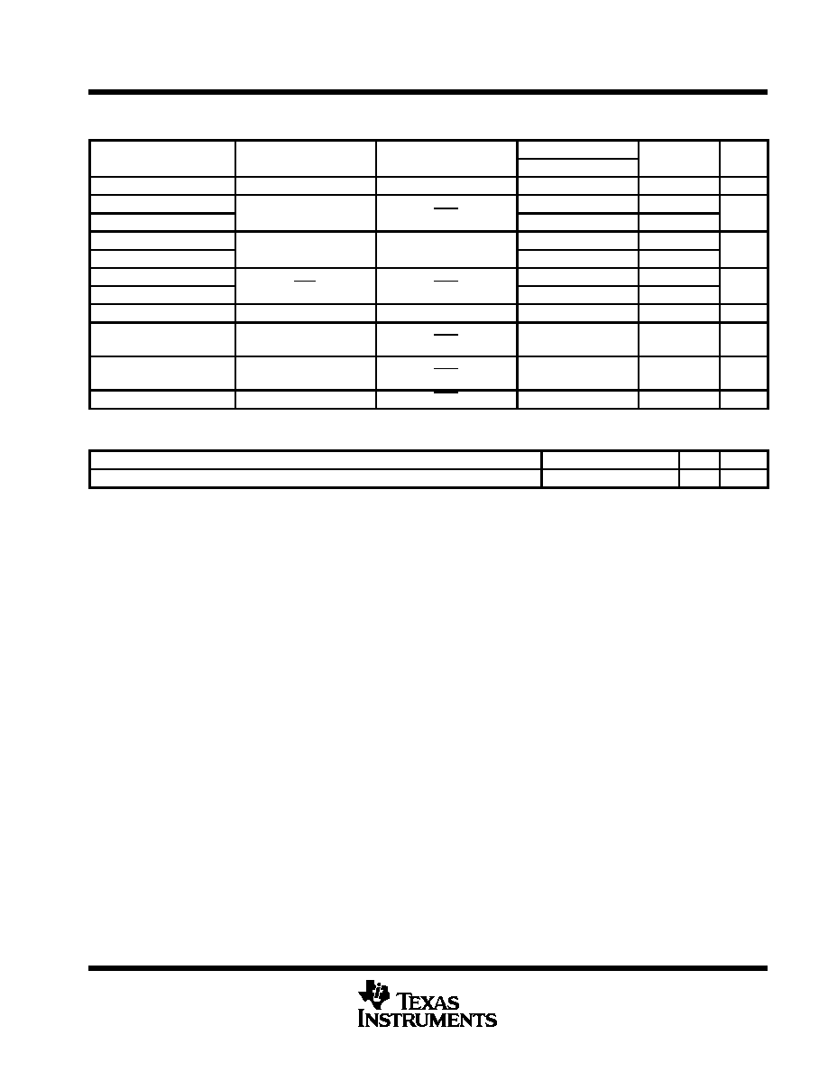
recommended operating conditions (see Note 3)
MIN
NOM
MAX
UNIT
VCC
Supply voltage
4.5
5
5.5
V
VIH
High-level input voltage
2
V
VIL
Low-level input voltage
0.8
V
VI
Input voltage
0
VCC
V
VO
Output voltage
0
VCC
V
IOH
High-level output current
≠24
mA
IOL
Low-level output current
24
mA
t/
v
Input transition rise or fall rate
0
10
ns/V
TA
Operating free-air temperature
≠40
85
∞
C
NOTE 3: All unused inputs of the device must be held at VCC or GND to ensure proper device operation. Refer to the TI application report,
Implications of Slow or Floating CMOS Inputs, literature number SCBA004.

74ACT11867
SYNCHRONOUS 8-BIT UP/DOWN BINARY COUNTER
WITH ASYNCHRONOUS CLEAR
SCAS178A ≠ DECEMBER 1991 ≠ REVISED FEBRUARY 1998
6
POST OFFICE BOX 655303
∑
DALLAS, TEXAS 75265
electrical characteristics over recommended operating free-air temperature range (unless
otherwise noted)
PARAMETER
TEST CONDITIONS
VCC
TA = 25
∞
C
MIN
MAX
UNIT
PARAMETER
TEST CONDITIONS
VCC
MIN
TYP
MAX
MIN
MAX
UNIT
IOH = 50
µ
A
4.5 V
4.4
4.4
IOH = ≠50
µ
A
5.5 V
5.4
5.4
VOH
IOH = ≠24 mA
4.5 V
3.94
3.8
V
OH
5.5 V
4.94
4.8
IOH = ≠75 mA
5.5 V
3.85
IOL = 50
µ
A
4.5 V
0.1
0.1
IOL = 50
µ
A
5.5 V
0.1
0.1
VOL
IOL = 24 mA
4.5 V
0.36
0.44
V
IOL = 24 mA
5.5 V
0.36
0.44
IOL = 75 mA
5.5 V
1.65
II
VI = VCC or GND
5.5 V
±
0.1
±
1
µ
A
ICC
VI = VCC or GND,
IO = 0
5.5 V
8
80
µ
A
ICC
One input at 3.4 V,
Other inputs at VCC or GND
5.5 V
0.9
1
mA
Ci
VI = VCC or GND
5 V
4.5
pF
Not more than one output should be tested at a time, and the duration of the test should not exceed 10 ms.
This is the increase in supply current for each input that is at one of the specified TTL voltage levels rather than 0 V or VCC.
timing requirements over recommended operating free-air temperature range, V
CC
= 5 V
±
0.5 V
(unless otherwise noted) (see Figure 1)
TA = 25
∞
C
MIN
MAX
UNIT
MIN
MAX
MIN
MAX
UNIT
fclock
Clock frequency
0
70
0
70
MHz
t
Pulse duration
S0 and S1 low
12
12
ns
tw
Pulse duration
CLK
6.5
6.5
ns
ß
Data
8
8
ß
ENP, ENT
4
4
tsuß
Setup time before CLK
S0, S1 (load)
11
11
ns
S0, S1 (count down)
11
11
S0, S1 (count up)
11
11
th
Hold time after CLK
Data
1
1
ns
tskew
Skew time between S0 and S1 to avoid inadvertent clear∂
S0 and S1 low
0
0
ns
ß This setup time is required to ensure stable data.
∂ This is the maximum time for which S0 and S1 can be low simultaneously when the device transitions between the load (S1 = H, S0 = L) and
count-down (S1 = L, S0 = H) modes.
74ACT11867
SYNCHRONOUS 8-BIT UP/DOWN BINARY COUNTER
WITH ASYNCHRONOUS CLEAR
SCAS178A ≠ DECEMBER 1991 ≠ REVISED FEBRUARY 1998
7
POST OFFICE BOX 655303
∑
DALLAS, TEXAS 75265
switching characteristics over recommended operating free-air temperature range,
V
CC
= 5 V
±
0.5 V (unless otherwise noted) (see Figure 1)
PARAMETER
FROM
TO
TA = 25
∞
C
MIN
MAX
UNIT
PARAMETER
(INPUT)
(OUTPUT)
MIN
TYP
MAX
MIN
MAX
UNIT
fmax
70
70
MHz
tPLH
CLK
RCO
6
9.9
12.7
6
14.6
ns
tPHL
CLK
RCO
6.4
10.9
14.2
6.4
16.3
ns
tPLH
CLK
Q
5
8.9
11.9
5
13.6
ns
tPHL
CLK
Q
4.9
9
12.2
4.9
14
ns
tPLH
ENT
RCO
3.9
6.8
9.1
3.9
10.5
ns
tPHL
ENT
RCO
3.1
7
10.2
3.1
11.5
ns
tPHL
Clear (S0, S1 low)
Q
6.3
11.9
16.6
6.3
19.1
ns
tPLH
S0, S1
RCO
5 5
10 4
15 6
5 5
17 8
ns
tPLH
,
(count up/down)
RCO
5.5
10.4
15.6
5.5
17.8
ns
tPHL
S0, S1
RCO
5 6
10 1
14 8
5 6
17 2
ns
tPHL
,
(count up/down)
RCO
5.6
10.1
14.8
5.6
17.2
ns
tPHL
Clear (S0, S1 low)
RCO
6.2
11.3
15.6
6.2
17.8
ns
operating characteristics, V
CC
= 5 V, T
A
= 25
∞
C
PARAMETER
TEST CONDITIONS
TYP
UNIT
Cpd
Power dissipation capacitance
CL = 50 pF,
f = 1 MHz
62
pF
74ACT11867
SYNCHRONOUS 8-BIT UP/DOWN BINARY COUNTER
WITH ASYNCHRONOUS CLEAR
SCAS178A ≠ DECEMBER 1991 ≠ REVISED FEBRUARY 1998
8
POST OFFICE BOX 655303
∑
DALLAS, TEXAS 75265
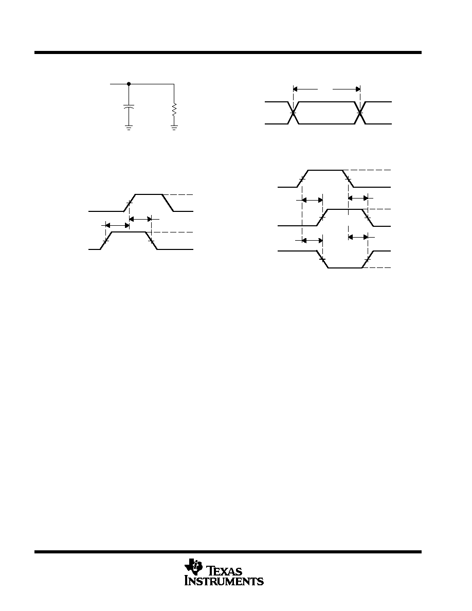
PARAMETER MEASUREMENT INFORMATION
50% VCC
1.5 V
1.5 V
1.5 V
3 V
3 V
0 V
0 V
th
tsu
VOLTAGE WAVEFORMS
Data Input
tPLH
tPHL
tPHL
tPLH
VOH
VOL
VOL
1.5 V
1.5 V
3 V
0 V
50% VCC
50% VCC
Input
(see Note B)
Out-of-Phase
Output
In-Phase
Output
Timing Input
(see Note B)
VOLTAGE WAVEFORMS
3 V
0 V
1.5 V
1.5 V
tw
VOLTAGE WAVEFORMS
Input
LOAD CIRCUIT
From Output
Under Test
CL = 50 pF
(see Note A)
500
NOTES: A. CL includes probe and jig capacitance.
B. All input pulses are supplied by generators having the following characteristics: PRR
10 MHz, ZO = 50
, tr = 3 ns, tf = 3 ns.
C. The outputs are measured one at a time with one input transition per measurement.
50% VCC
VOH
Figure 1. Load Circuit and Voltage Waveforms

IMPORTANT NOTICE
Texas Instruments and its subsidiaries (TI) reserve the right to make changes to their products or to discontinue
any product or service without notice, and advise customers to obtain the latest version of relevant information
to verify, before placing orders, that information being relied on is current and complete. All products are sold
subject to the terms and conditions of sale supplied at the time of order acknowledgement, including those
pertaining to warranty, patent infringement, and limitation of liability.
TI warrants performance of its semiconductor products to the specifications applicable at the time of sale in
accordance with TI's standard warranty. Testing and other quality control techniques are utilized to the extent
TI deems necessary to support this warranty. Specific testing of all parameters of each device is not necessarily
performed, except those mandated by government requirements.
CERTAIN APPLICATIONS USING SEMICONDUCTOR PRODUCTS MAY INVOLVE POTENTIAL RISKS OF
DEATH, PERSONAL INJURY, OR SEVERE PROPERTY OR ENVIRONMENTAL DAMAGE ("CRITICAL
APPLICATIONS"). TI SEMICONDUCTOR PRODUCTS ARE NOT DESIGNED, AUTHORIZED, OR
WARRANTED TO BE SUITABLE FOR USE IN LIFE-SUPPORT DEVICES OR SYSTEMS OR OTHER
CRITICAL APPLICATIONS. INCLUSION OF TI PRODUCTS IN SUCH APPLICATIONS IS UNDERSTOOD TO
BE FULLY AT THE CUSTOMER'S RISK.
In order to minimize risks associated with the customer's applications, adequate design and operating
safeguards must be provided by the customer to minimize inherent or procedural hazards.
TI assumes no liability for applications assistance or customer product design. TI does not warrant or represent
that any license, either express or implied, is granted under any patent right, copyright, mask work right, or other
intellectual property right of TI covering or relating to any combination, machine, or process in which such
semiconductor products or services might be or are used. TI's publication of information regarding any third
party's products or services does not constitute TI's approval, warranty or endorsement thereof.
Copyright
©
1998, Texas Instruments Incorporated