SN74ALVCH16835
18 BIT UNIVERSAL BUS DRIVER
WITH 3 STATE OUTPUTS
SCES053I - SEPTEMBER 1995 - REVISED AUGUST 2003
1
POST OFFICE BOX 655303
∑
DALLAS, TEXAS 75265
D
Member of the Texas Instruments
Widebus
Family
D
Operates From 1.65 V to 3.6 V
D
Max t
pd
of 3.6 ns at 3.3 V
D
±
24-mA Output Drive at 3.3 V
D
Bus Hold on Data Inputs Eliminates the
Need for External Pullup/Pulldown
Resistors
D
Latch-Up Performance Exceeds 250 mA Per
JESD 17
D
ESD Protection Exceeds JESD 22
- 2000-V Human-Body Model (A114-A)
- 200-V Machine Model (A115-A)
description/ordering information
This 18-bit universal bus driver is designed for
1.65-V to 3.6-V V
CC
operation.
Data flow from A to Y is controlled by the
output-enable (OE) input. The device operates in
the transparent mode when the latch-enable (LE)
input is high. The A data is latched if the clock
(CLK) input is held at a high or low logic level. If LE
is low, the A data is stored in the latch/flip-flop on
the low-to-high transition of CLK. When OE is
high, the outputs are in the high-impedance state.
To ensure the high-impedance state during power
up or power down, OE should be tied to V
CC
through a pullup resistor; the minimum value of
the resistor is determined by the current-sinking
capability of the driver.
Active bus-hold circuitry holds unused or undriven inputs at a valid logic state. Use of pullup or pulldown resistors
with the bus-hold circuitry is not recommended.
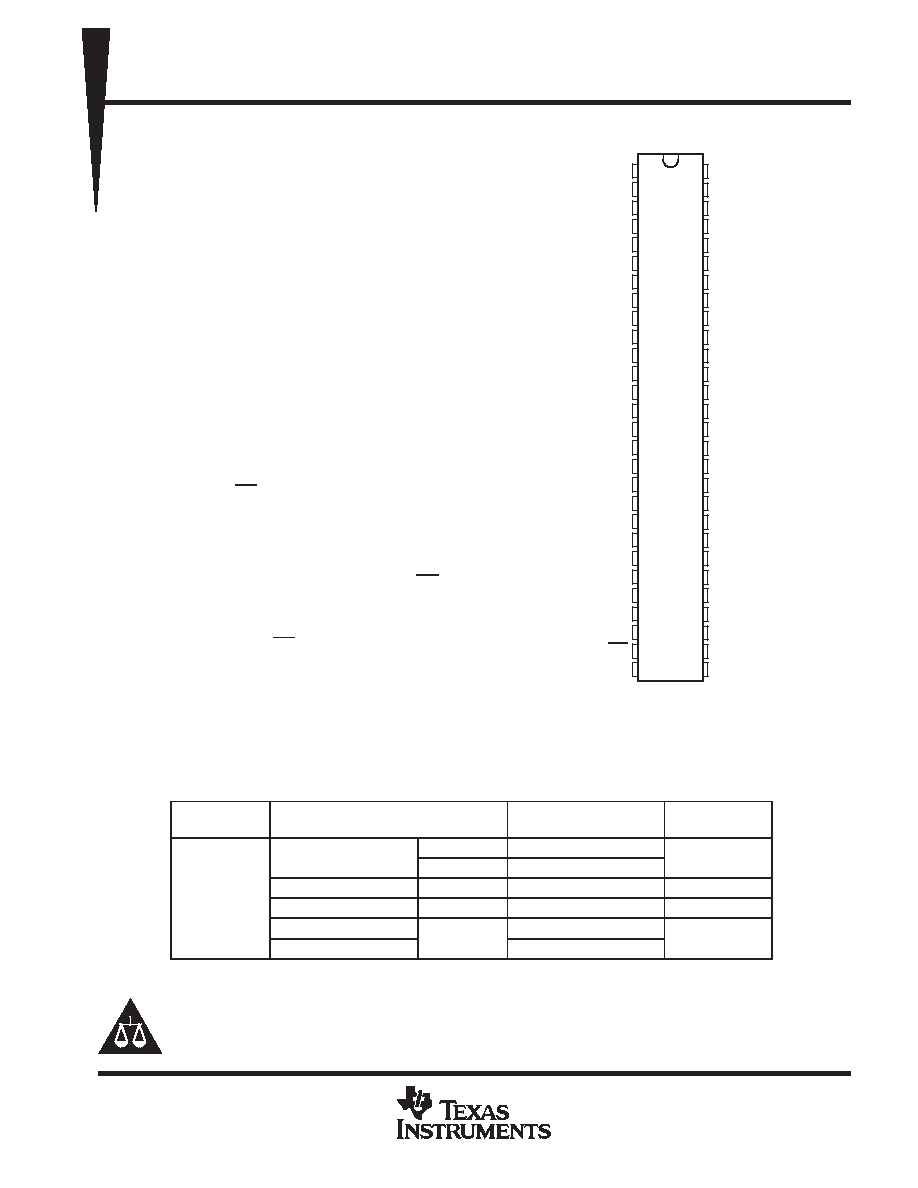
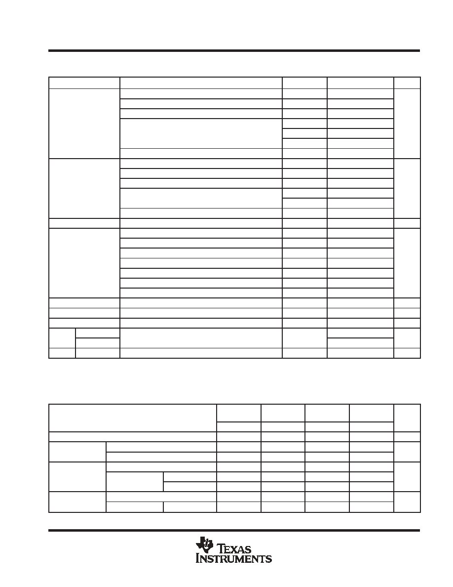
ORDERING INFORMATION
TA
PACKAGE
ORDERABLE
PART NUMBER
TOP-SIDE
MARKING
SSOP - DL
Tube
SN74ALVCH16835DL
ALVCH16835
SSOP - DL
Tape and reel
SN74ALVCH16835DLR
ALVCH16835
-40
∞
C to 85
∞
C
TSSOP - DGG
Tape and reel
SN74ALVCH16835DGGR
ALVCH16835
-40
∞
C to 85
∞
C
TVSOP - DGV
Tape and reel
SN74ALVCH16835DGVR
VH835
VFBGA - GQL
Tape and reel
SN74ALVCH16835KR
VH835
VFBGA - ZQL (Pb-free)
Tape and reel
74ALVCH16835ZQLR
VH835
Package drawings, standard packing quantities, thermal data, symbolization, and PCB design guidelines are
available at www.ti.com/sc/package.
Copyright
2003, Texas Instruments Incorporated
PRODUCTION DATA information is current as of publication date.
Products conform to specifications per the terms of Texas Instruments
standard warranty. Production processing does not necessarily include
testing of all parameters.
Please be aware that an important notice concerning availability, standard warranty, and use in critical applications of
Texas Instruments semiconductor products and disclaimers thereto appears at the end of this data sheet.
Widebus is a trademark of Texas Instruments.
1
2
3
4
5
6
7
8
9
10
11
12
13
14
15
16
17
18
19
20
21
22
23
24
25
26
27
28
56
55
54
53
52
51
50
49
48
47
46
45
44
43
42
41
40
39
38
37
36
35
34
33
32
31
30
29
NC
NC
Y1
GND
Y2
Y3
V
CC
Y4
Y5
Y6
GND
Y7
Y8
Y9
Y10
Y11
Y12
GND
Y13
Y14
Y15
V
CC
Y16
Y17
GND
Y18
OE
LE
GND
NC
A1
GND
A2
A3
V
CC
A4
A5
A6
GND
A7
A8
A9
A10
A11
A12
GND
A13
A14
A15
V
CC
A16
A17
GND
A18
CLK
GND
DGG, DGV, OR DL PACKAGE
(TOP VIEW)
NC - No internal connection
SN74ALVCH16835
18 BIT UNIVERSAL BUS DRIVER
WITH 3 STATE OUTPUTS
SCES053I - SEPTEMBER 1995 - REVISED AUGUST 2003
2
POST OFFICE BOX 655303
∑
DALLAS, TEXAS 75265
terminal assignments
1
2
3
4
5
6
A
Y1
NC
NC
GND
NC
A1
B
Y3
Y2
GND
GND
A2
A3
C
Y5
Y4
VCC
VCC
A4
A5
D
Y7
Y6
GND
GND
A6
A7
E
Y9
Y8
A8
A9
F
Y10
Y11
A11
A10
G
Y12
Y13
GND
GND
A13
A12
H
Y14
Y15
VCC
VCC
A15
A14
J
Y16
Y17
GND
GND
A17
A16
K
Y18
OE
LE
GND
CLK
A18
NC - No internal connection
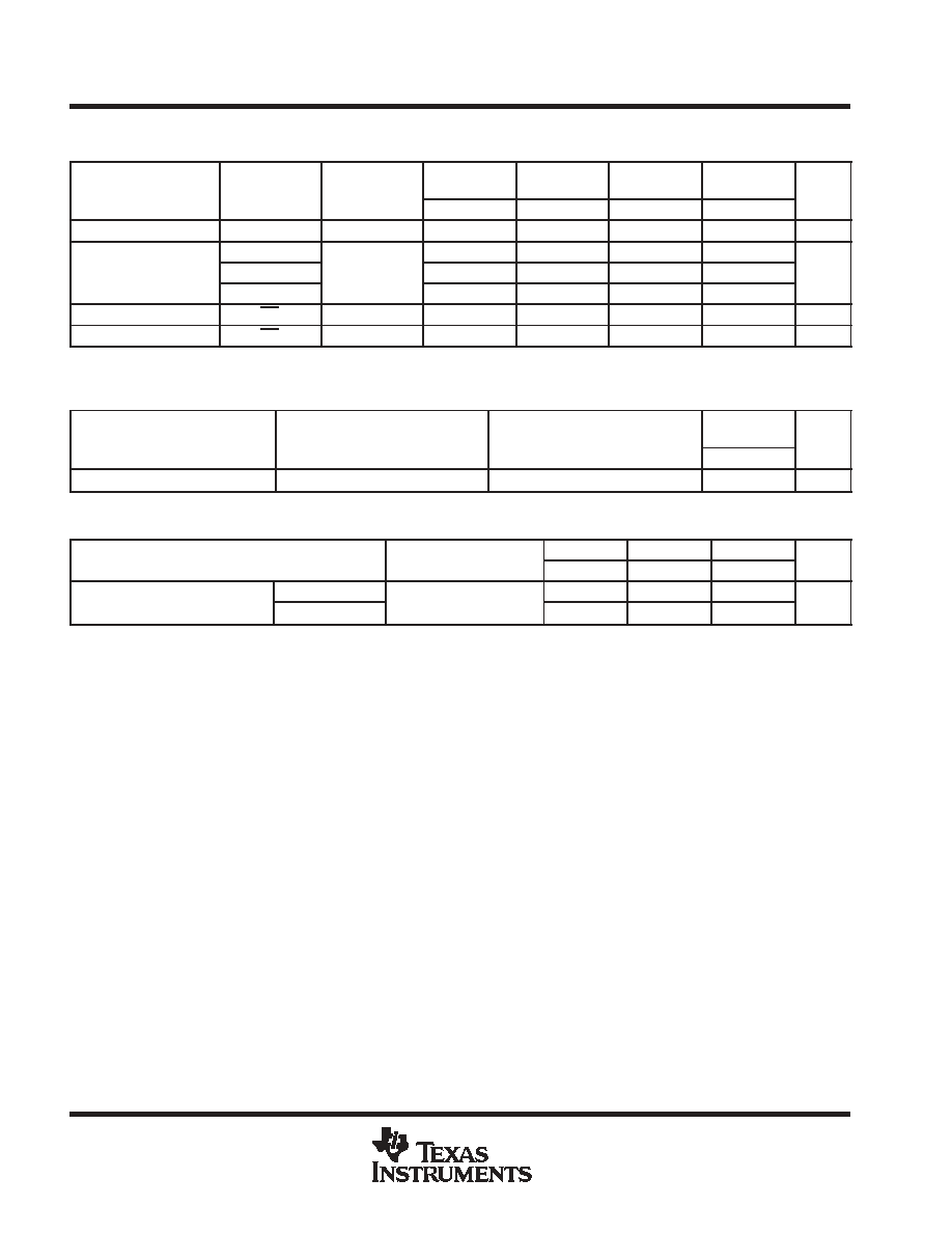
FUNCTION TABLE
INPUTS
OUTPUT
OE
LE
CLK
A
OUTPUT
Y
H
X
X
X
Z
L
H
X
L
L
L
H
X
H
H
L
L
L
L
L
L
H
H
L
L
H
X
Y0
L
L
L
X
Y0
Output level before the indicated steady-state
input conditions were established, provided
that CLK is high before LE goes low
Output level before the indicated steady-state
input conditions were established
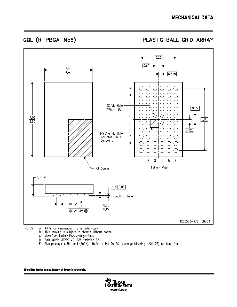
GQL OR ZQL PACKAGE
(TOP VIEW)
J
H
G
F
E
D
C
B
A
2
1
3
4
6
5
K
SN74ALVCH16835
18 BIT UNIVERSAL BUS DRIVER
WITH 3 STATE OUTPUTS
SCES053I - SEPTEMBER 1995 - REVISED AUGUST 2003
3
POST OFFICE BOX 655303
∑
DALLAS, TEXAS 75265
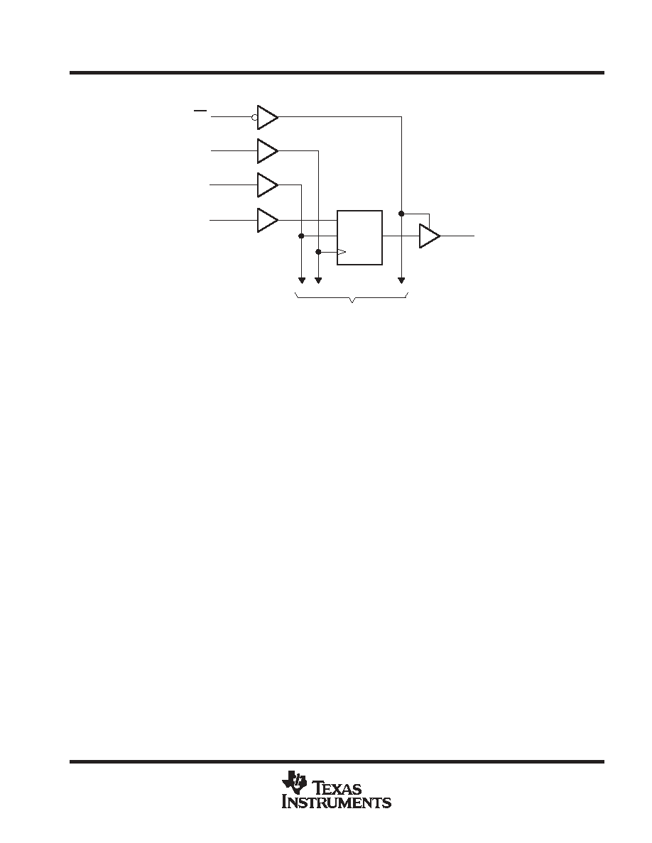
logic diagram (positive logic)
OE
CLK
Y1
1D
C1
CLK
To 17 Other Channels
LE
A1
27
30
28
54
3
Pin numbers shown are for the DGG, DGV, and DL packages.
absolute maximum ratings over operating free-air temperature range (unless otherwise noted)
Supply voltage range, V
CC
-0.5 V to 4.6 V
. . . . . . . . . . . . . . . . . . . . . . . . . . . . . . . . . . . . . . . . . . . . . . . . . . . . . . . . .
Input voltage range, V
I
(see Note 1)
-0.5 V to 4.6 V
. . . . . . . . . . . . . . . . . . . . . . . . . . . . . . . . . . . . . . . . . . . . . . . . .
Output voltage range, V
O
(see Notes 1 and 2)
-0.5 V to V
CC
+ 0.5 V
. . . . . . . . . . . . . . . . . . . . . . . . . . . . . . . . . .
Input clamp current, I
IK
(V
I
< 0)
-50 mA
. . . . . . . . . . . . . . . . . . . . . . . . . . . . . . . . . . . . . . . . . . . . . . . . . . . . . . . . . . .
Output clamp current, I
OK
(V
O
< 0)
-50 mA
. . . . . . . . . . . . . . . . . . . . . . . . . . . . . . . . . . . . . . . . . . . . . . . . . . . . . . . .
Continuous output current, I
O
±
50 mA
. . . . . . . . . . . . . . . . . . . . . . . . . . . . . . . . . . . . . . . . . . . . . . . . . . . . . . . . . . . . .
Continuous current through each V
CC
or GND
±
100 mA
. . . . . . . . . . . . . . . . . . . . . . . . . . . . . . . . . . . . . . . . . . . . .
Package thermal impedance,
JA
(see Note 3): DGG package
64
∞
C/W
. . . . . . . . . . . . . . . . . . . . . . . . . . . . . . .
DGV package
48
∞
C/W
. . . . . . . . . . . . . . . . . . . . . . . . . . . . . . . .
DL package
56
∞
C/W
. . . . . . . . . . . . . . . . . . . . . . . . . . . . . . . . .
GQL/ZQL package
42
∞
C/W
. . . . . . . . . . . . . . . . . . . . . . . . . . .
Storage temperature range, T
stg
-65
∞
C to 150
∞
C
. . . . . . . . . . . . . . . . . . . . . . . . . . . . . . . . . . . . . . . . . . . . . . . . . . .
Stresses beyond those listed under "absolute maximum ratings" may cause permanent damage to the device. These are stress ratings only, and
functional operation of the device at these or any other conditions beyond those indicated under "recommended operating conditions" is not
implied. Exposure to absolute-maximum-rated conditions for extended periods may affect device reliability.
NOTES:
1. The input negative-voltage and output voltage ratings may be exceeded if the input and output current ratings are observed.
2. This value is limited to 4.6 V maximum.
3. The package thermal impedance is calculated in accordance with JESD 51-7.
SN74ALVCH16835
18 BIT UNIVERSAL BUS DRIVER
WITH 3 STATE OUTPUTS
SCES053I - SEPTEMBER 1995 - REVISED AUGUST 2003
4
POST OFFICE BOX 655303
∑
DALLAS, TEXAS 75265
recommended operating conditions (see Note 4)
MIN
MAX
UNIT
VCC
Supply voltage
1.65
3.6
V
VCC = 1.65 V to 1.95 V
0.65
◊
VCC
VIH
High-level input voltage
VCC = 2.3 V to 2.7 V
1.7
V
VIH
High-level input voltage
VCC = 2.7 V to 3.6 V
2
V
VCC = 1.65 V to 1.95 V
0.35
◊
VCC
VIL
Low-level input voltage
VCC = 2.3 V to 2.7 V
0.7
V
VIL
Low-level input voltage
VCC = 2.7 V to 3.6 V
0.8
V
VI
Input voltage
0
VCC
V
VO
Output voltage
0
VCC
V
VCC = 1.65 V
-4
IOH
High-level output current
VCC = 2.3 V
-12
mA
IOH
High-level output current
VCC = 2.7 V
-12
mA
VCC = 3 V
-24
VCC = 1.65 V
4
IOL
Low-level output current
VCC = 2.3 V
12
mA
IOL
Low-level output current
VCC = 2.7 V
12
mA
VCC = 3 V
24
t/
v
Input transition rise or fall rate
10
ns/V
TA
Operating free-air temperature
-40
85
∞
C
NOTE 4: All unused control inputs of the device must be held at VCC or GND to ensure proper device operation. Refer to the TI application report,
Implications of Slow or Floating CMOS Inputs, literature number SCBA004.
SN74ALVCH16835
18 BIT UNIVERSAL BUS DRIVER
WITH 3 STATE OUTPUTS
SCES053I - SEPTEMBER 1995 - REVISED AUGUST 2003
5
POST OFFICE BOX 655303
∑
DALLAS, TEXAS 75265
electrical characteristics over recommended operating free-air temperature range (unless
otherwise noted)
PARAMETER
TEST CONDITIONS
VCC
MIN
TYP
MAX
UNIT
IOH = -100
µ
A
1.65 V to 3.6 V
VCC-0.2
IOH = -4 mA
1.65 V
1.2
IOH = -6 mA
2.3 V
2
VOH
2.3 V
1.7
V
VOH
IOH = -12 mA
2.7 V
2.2
V
IOH = -12 mA
3 V
2.4
IOH = -24 mA
3 V
2
IOL = 100
µ
A
1.65 V to 3.6 V
0.2
IOL = 4 mA
1.65 V
0.45
VOL
IOL = 6 mA
2.3 V
0.4
V
VOL
IOL = 12 mA
2.3 V
0.7
V
IOL = 12 mA
2.7 V
0.4
IOL = 24 mA
3 V
0.55
II
VI = VCC or GND
3.6 V
±
5
µ
A
VI = 0.58 V
1.65 V
25
VI = 1.07 V
1.65 V
-25
VI = 0.7 V
2.3 V
45
II(hold)
VI = 1.7 V
2.3 V
-45
µ
A
II(hold)
VI = 0.8 V
3 V
75
µ
A
VI = 2 V
3 V
-75
VI = 0 to 3.6 V
3.6 V
±
500
IOZ
VO = VCC or GND
3.6 V
±
10
µ
A
ICC
VI = VCC or GND,
IO = 0
3.6 V
40
µ
A
ICC
One input at VCC - 0.6 V,
Other inputs at VCC or GND
3 V to 3.6 V
750
µ
A
Ci
Control inputs
VI = VCC or GND
3.3 V
3.5
pF
Ci
Data inputs
VI = VCC or GND
3.3 V
6
pF
Co
Outputs
VO = VCC or GND
3.3 V
7
pF
All typical values are at VCC = 3.3 V, TA = 25
∞
C.
This is the bus-hold maximum dynamic current. It is the minimum overdrive current required to switch the input from one state to another.
timing requirements over recommended operating free-air temperature range (unless otherwise
noted) (see Figure 1)
VCC = 1.8 V
VCC = 2.5 V
±
0.2 V
VCC = 2.7 V
VCC = 3.3 V
±
0.3 V
UNIT
MIN
TYP
MIN
MAX
MIN
MAX
MIN
MAX
UNIT
fclock
Clock frequency
ß
150
150
150
MHz
tw
Pulse
LE high
ß
3.3
3.3
3.3
ns
tw
Pulse
duration
CLK high or low
ß
3.3
3.3
3.3
ns
Setup
Data before CLK
ß
2.2
2.1
1.7
tsu
Setup
time
Data before LE
CLK high
ß
1.9
1.6
1.5
ns
tsu
time
Data before LE
CLK low
ß
1.3
1.1
1
ns
th
Hold
Data after CLK
ß
0.6
0.6
0.7
ns
th
Hold
time
Data after LE
CLK high or low
ß
1.4
1.7
1.4
ns
ß This information was not available at the time of publication.
SN74ALVCH16835
18 BIT UNIVERSAL BUS DRIVER
WITH 3 STATE OUTPUTS
SCES053I - SEPTEMBER 1995 - REVISED AUGUST 2003
6
POST OFFICE BOX 655303
∑
DALLAS, TEXAS 75265
switching characteristics over recommended operating free-air temperature range (unless
otherwise noted) (see Figure 1)
PARAMETER
FROM
(INPUT)
TO
(OUTPUT)
VCC = 1.8 V
VCC = 2.5 V
±
0.2 V
VCC = 2.7 V
VCC = 3.3 V
±
0.3 V
UNIT
PARAMETER
(INPUT)
(OUTPUT)
MIN
TYP
MIN
MAX
MIN
MAX
MIN
MAX
UNIT
fmax
150
150
150
MHz
A
1
4.2
4.2
1
3.6
tpd
LE
Y
1.3
5
4.9
1.3
4.2
ns
tpd
CLK
Y
1.4
5.5
5.2
1.4
4.5
ns
ten
OE
Y
1.4
5.5
5.6
1.1
4.6
ns
tdis
OE
Y
1
4.5
4.3
1.3
3.9
ns
This information was not available at the time of publication.
switching characteristics from 0
∞
C to 65
∞
C, C
L
= 50 pF
PARAMETER
FROM
(INPUT)
TO
(OUTPUT)
VCC = 3.3 V
±
0.15 V
UNIT
PARAMETER
(INPUT)
(OUTPUT)
MIN
MAX
UNIT
tpd
CLK
Y
1.7
4.5
ns
operating characteristics, T
A
= 25
∞
C
PARAMETER
TEST CONDITIONS
VCC = 1.8 V VCC = 2.5 V VCC = 3.3 V
UNIT
PARAMETER
TEST CONDITIONS
TYP
TYP
TYP
UNIT
Cpd
Power dissipation
Outputs enabled
CL = 50 pF,
f = 10 MHz
26
31
pF
Cpd
Power dissipation
capacitance
Outputs disabled
CL = 50 pF,
f = 10 MHz
12
14
pF
This information was not available at the time of publication.
SN74ALVCH16835
18 BIT UNIVERSAL BUS DRIVER
WITH 3 STATE OUTPUTS
SCES053I - SEPTEMBER 1995 - REVISED AUGUST 2003
7
POST OFFICE BOX 655303
∑
DALLAS, TEXAS 75265
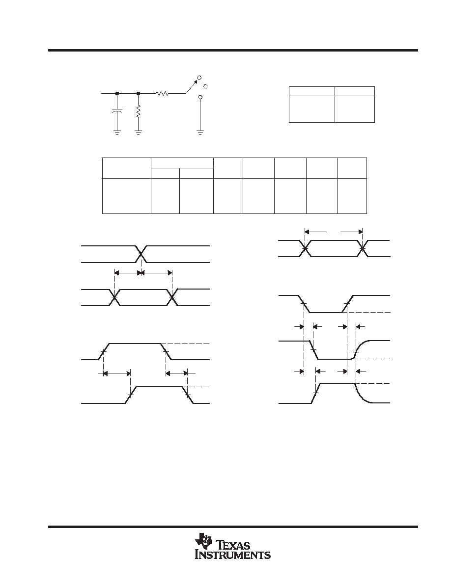
PARAMETER MEASUREMENT INFORMATION
VM
VM
VM
VM
VM
VM
VM
VM
VOH
VOL
th
tsu
From Output
Under Test
CL
(see Note A)
LOAD CIRCUIT
S1
Open
GND
RL
RL
Output
Control
(low-level
enabling)
Output
Waveform 1
S1 at VLOAD
(see Note B)
Output
Waveform 2
S1 at GND
(see Note B)
tPZL
tPZH
tPLZ
tPHZ
0 V
VOL + V
VOH - V
0 V
VI
0 V
0 V
tw
VI
VI
VOLTAGE WAVEFORMS
SETUP AND HOLD TIMES
VOLTAGE WAVEFORMS
PULSE DURATION
VOLTAGE WAVEFORMS
ENABLE AND DISABLE TIMES
Timing
Input
Data
Input
Input
tpd
tPLZ/tPZL
tPHZ/tPZH
Open
VLOAD
GND
TEST
S1
NOTES: A. CL includes probe and jig capacitance.
B. Waveform 1 is for an output with internal conditions such that the output is low except when disabled by the output control.
Waveform 2 is for an output with internal conditions such that the output is high except when disabled by the output control.
C. All input pulses are supplied by generators having the following characteristics: PRR
10 MHz, ZO = 50
.
D. The outputs are measured one at a time with one transition per measurement.
E. tPLZ and tPHZ are the same as tdis.
F. tPZL and tPZH are the same as ten.
G. tPLH and tPHL are the same as tpd.
H. All parameters and waveforms are not applicable to all devices.
0 V
VI
VM
tPHL
VM
VM
VI
0 V
VOH
VOL
Input
Output
VOLTAGE WAVEFORMS
PROPAGATION DELAY TIMES
VM
VM
tPLH
VLOAD
VLOAD/2
1.8 V
2.5 V
±
0.2 V
2.7 V
3 V
±
0.3 V
1 k
500
500
500
VCC
RL
2
◊
VCC
2
◊
VCC
6 V
6 V
VLOAD
CL
30 pF
30 pF
50 pF
50 pF
0.15 V
0.15 V
0.3 V
0.3 V
V
VCC
VCC
2.7 V
2.7 V
VI
VCC/2
VCC/2
1.5 V
1.5 V
VM
tr/tf
2 ns
2 ns
2.5 ns
2.5 ns
INPUT
Figure 1. Load Circuit and Voltage Waveforms
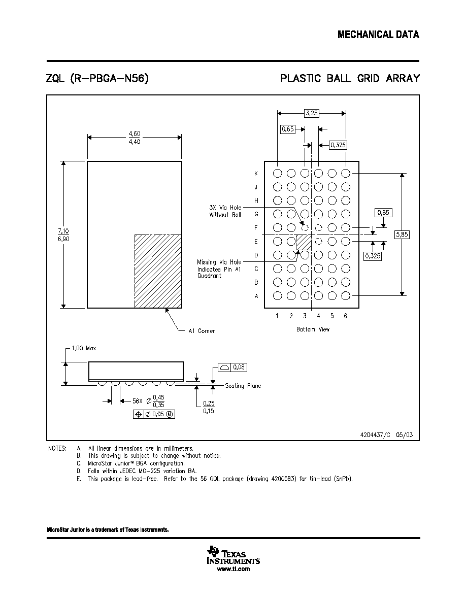
MECHANICAL DATA
MPDS006C ≠ FEBRUARY 1996 ≠ REVISED AUGUST 2000
POST OFFICE BOX 655303
∑
DALLAS, TEXAS 75265
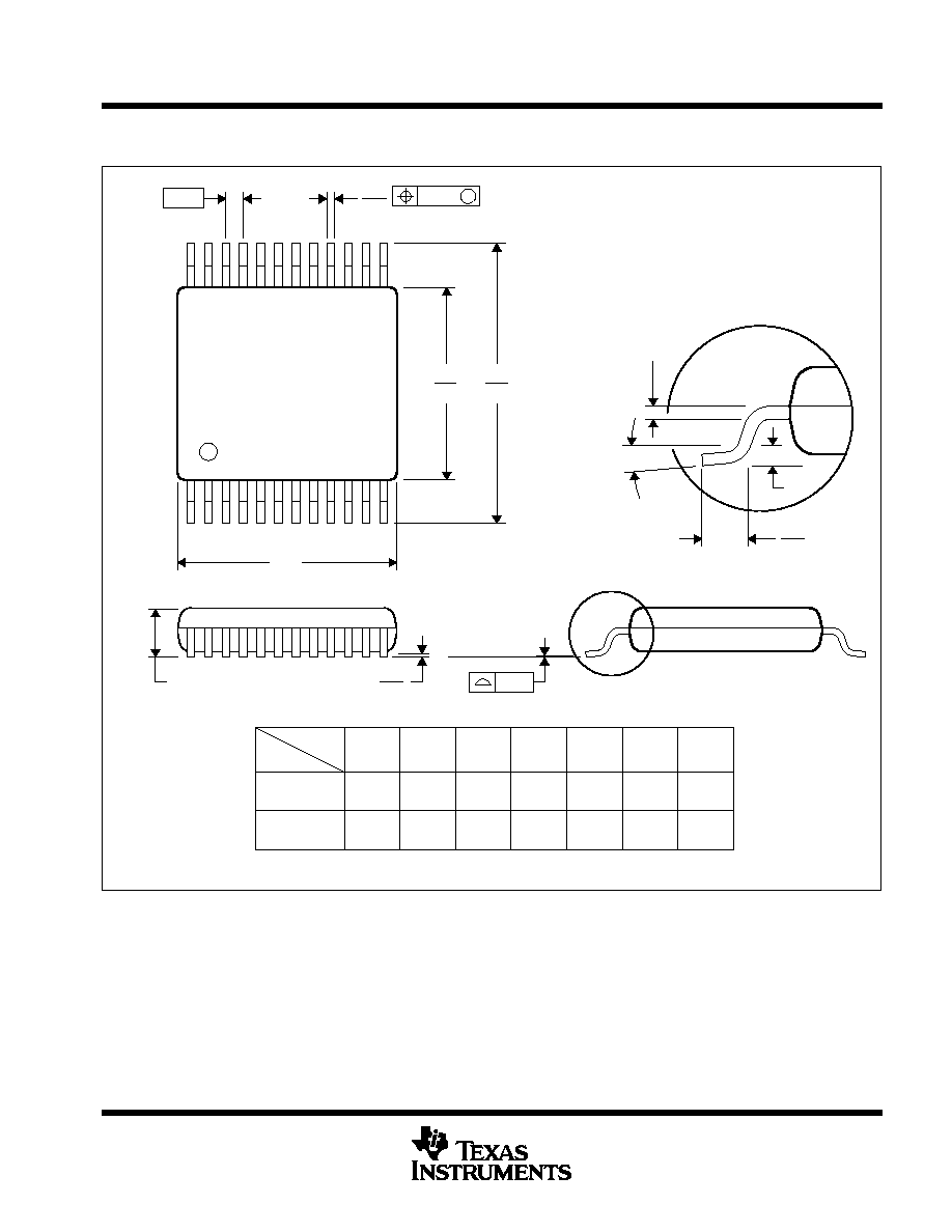
DGV (R-PDSO-G**)
PLASTIC SMALL-OUTLINE
24 PINS SHOWN
14
3,70
3,50
4,90
5,10
20
DIM
PINS **
4073251/E 08/00
1,20 MAX
Seating Plane
0,05
0,15
0,25
0,50
0,75
0,23
0,13
1
12
24
13
4,30
4,50
0,16 NOM
Gage Plane
A
7,90
7,70
38
24
16
4,90
5,10
3,70
3,50
A MAX
A MIN
6,60
6,20
11,20
11,40
56
9,60
9,80
48
0,08
M
0,07
0,40
0
∞
≠ 8
∞
NOTES: A. All linear dimensions are in millimeters.
B. This drawing is subject to change without notice.
C. Body dimensions do not include mold flash or protrusion, not to exceed 0,15 per side.
D. Falls within JEDEC: 24/48 Pins ≠ MO-153
14/16/20/56 Pins ≠ MO-194
MECHANICAL DATA
MSSO001C ≠ JANUARY 1995 ≠ REVISED DECEMBER 2001
POST OFFICE BOX 655303
∑
DALLAS, TEXAS 75265
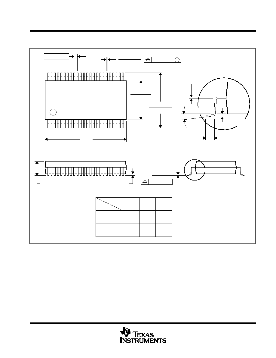
DL (R-PDSO-G**)
PLASTIC SMALL-OUTLINE PACKAGE
4040048 / E 12/01
48 PINS SHOWN
56
0.730
(18,54)
0.720
(18,29)
48
28
0.370
(9,40)
(9,65)
0.380
Gage Plane
DIM
0.420 (10,67)
0.395 (10,03)
A MIN
A MAX
0.010 (0,25)
PINS **
0.630
(16,00)
(15,75)
0.620
0.010 (0,25)
Seating Plane
0.020 (0,51)
0.040 (1,02)
25
24
0.008 (0,203)
0.0135 (0,343)
48
1
0.008 (0,20) MIN
A
0.110 (2,79) MAX
0.299 (7,59)
0.291 (7,39)
0.004 (0,10)
M
0.005 (0,13)
0.025 (0,635)
0
∞
≠ 8
∞
0.005 (0,13)
NOTES: A. All linear dimensions are in inches (millimeters).
B. This drawing is subject to change without notice.
C. Body dimensions do not include mold flash or protrusion not to exceed 0.006 (0,15).
D. Falls within JEDEC MO-118
MECHANICAL DATA
MTSS003D ≠ JANUARY 1995 ≠ REVISED JANUARY 1998
POST OFFICE BOX 655303
∑
DALLAS, TEXAS 75265
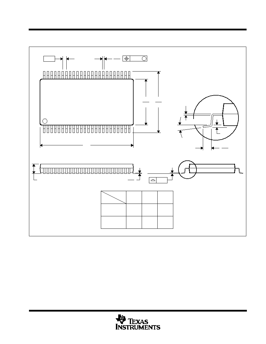
DGG (R-PDSO-G**)
PLASTIC SMALL-OUTLINE PACKAGE
4040078 / F 12/97
48 PINS SHOWN
0,25
0,15 NOM
Gage Plane
6,00
6,20
8,30
7,90
0,75
0,50
Seating Plane
25
0,27
0,17
24
A
48
1
1,20 MAX
M
0,08
0,10
0,50
0
∞
≠ 8
∞
56
14,10
13,90
48
DIM
A MAX
A MIN
PINS **
12,40
12,60
64
17,10
16,90
0,15
0,05
NOTES: A. All linear dimensions are in millimeters.
B. This drawing is subject to change without notice.
C. Body dimensions do not include mold protrusion not to exceed 0,15.
D. Falls within JEDEC MO-153

IMPORTANT NOTICE
Texas Instruments Incorporated and its subsidiaries (TI) reserve the right to make corrections, modifications,
enhancements, improvements, and other changes to its products and services at any time and to discontinue
any product or service without notice. Customers should obtain the latest relevant information before placing
orders and should verify that such information is current and complete. All products are sold subject to TI's terms
and conditions of sale supplied at the time of order acknowledgment.
TI warrants performance of its hardware products to the specifications applicable at the time of sale in
accordance with TI's standard warranty. Testing and other quality control techniques are used to the extent TI
deems necessary to support this warranty. Except where mandated by government requirements, testing of all
parameters of each product is not necessarily performed.
TI assumes no liability for applications assistance or customer product design. Customers are responsible for
their products and applications using TI components. To minimize the risks associated with customer products
and applications, customers should provide adequate design and operating safeguards.
TI does not warrant or represent that any license, either express or implied, is granted under any TI patent right,
copyright, mask work right, or other TI intellectual property right relating to any combination, machine, or process
in which TI products or services are used. Information published by TI regarding third-party products or services
does not constitute a license from TI to use such products or services or a warranty or endorsement thereof.
Use of such information may require a license from a third party under the patents or other intellectual property
of the third party, or a license from TI under the patents or other intellectual property of TI.
Reproduction of information in TI data books or data sheets is permissible only if reproduction is without
alteration and is accompanied by all associated warranties, conditions, limitations, and notices. Reproduction
of this information with alteration is an unfair and deceptive business practice. TI is not responsible or liable for
such altered documentation.
Resale of TI products or services with statements different from or beyond the parameters stated by TI for that
product or service voids all express and any implied warranties for the associated TI product or service and
is an unfair and deceptive business practice. TI is not responsible or liable for any such statements.
Following are URLs where you can obtain information on other Texas Instruments products and application
solutions:
Products
Applications
Amplifiers
amplifier.ti.com
Audio
www.ti.com/audio
Data Converters
dataconverter.ti.com
Automotive
www.ti.com/automotive
DSP
dsp.ti.com
Broadband
www.ti.com/broadband
Interface
interface.ti.com
Digital Control
www.ti.com/digitalcontrol
Logic
logic.ti.com
Military
www.ti.com/military
Power Mgmt
power.ti.com
Optical Networking
www.ti.com/opticalnetwork
Microcontrollers
microcontroller.ti.com
Security
www.ti.com/security
Telephony
www.ti.com/telephony
Video & Imaging
www.ti.com/video
Wireless
www.ti.com/wireless
Mailing Address:
Texas Instruments
Post Office Box 655303 Dallas, Texas 75265
Copyright
2003, Texas Instruments Incorporated