
SN74AVCH8T245
8 BIT DUAL SUPPLY BUS TRANSCEIVER
WITH CONFIGURABLE VOLTAGE TRANSLATION AND 3 STATE OUTPUTS
SCES565F - APRIL 2004 - REVISED APRIL 2005
1
POST OFFICE BOX 655303
∑
DALLAS, TEXAS 75265
D
Control Inputs V
IH
/V
IL
Levels Are
Referenced to V
CCA
Voltage
D
V
CC
Isolation Feature - If Either V
CC
Input
Is at GND, All I/O Ports Are in the
High-Impedance State
D
I
off
Supports Partial-Power-Down Mode
Operation
D
Fully Configurable Dual-Rail Design Allows
Each Port to Operate Over the Full 1.2-V to
3.6-V Power-Supply Range
D
I/Os Are 4.6-V Tolerant
D
Max Data Rates:
- 170 Mbps (1.2 V
3
(V
CCA
or V
CCB
)
3
3.3 V)
- 320 Mbps (1.8 V
3
(V
CCA
or V
CCB
)
3
3.3 V)
D
Bus Hold on Data Inputs Eliminates the
Need for External Pullup/Pulldown
Resistors
D
Latch-Up Performance Exceeds 100 mA Per
JESD 78, Class II
D
ESD Protection Exceeds JESD 22
- 8000-V Human-Body Model (A114-A)
- 200-V Machine Model (A115-A)
- 1000-V Charged-Device Model (C101)
DGV OR PW PACKAGE
(TOP VIEW)
1
2
3
4
5
6
7
8
9
10
11
12
24
23
22
21
20
19
18
17
16
15
14
13
V
CCA
DIR
A1
A2
A3
A4
A5
A6
A7
A8
GND
GND
V
CCB
V
CCB
OE
B1
B2
B3
B4
B5
B6
B7
B8
GND
RHL PACKAGE
(TOP VIEW)
1
24
12
13
2
3
4
5
6
7
8
9
10
11
23
22
21
20
19
18
17
16
15
14
V
CCB
OE
B1
B2
B3
B4
B5
B6
B7
B8
DIR
A1
A2
A3
A4
A5
A6
A7
A8
GND
GND
V
GND
CCB
V
CCA
description/ordering information
This 8-bit noninverting bus transceiver uses two separate configurable power-supply rails. The
SN74AVCH8T245 is optimized to operate with V
CCA
/V
CCB
set at 1.4 V to 3.6 V. It is operational with V
CCA
/V
CCB
as low as 1.2 V. The A port is designed to track V
CCA
. V
CCA
accepts any supply voltage from 1.2 V to 3.6 V. The
B port is designed to track V
CCB
. V
CCB
accepts any supply voltage from 1.2 V to 3.6 V. This allows for universal
low-voltage bidirectional translation between any of the 1.2-V, 1.5-V, 1.8-V, 2.5-V, and 3.3-V voltage nodes.
ORDERING INFORMATION
TA
PACKAGE
ORDERABLE
PART NUMBER
TOP-SIDE
MARKING
QFN - RHL
Tape and reel
SN74AVCH8T245RHLR
WP245
-40
∞
C to 85
∞
C
TSSOP - PW
Tube
SN74AVCH8T245PW
WP245
-40
∞
C to 85
∞
C
TSSOP - PW
Tape and reel
SN74AVCH8T245PWR
WP245
TVSOP - DGV
Tape and reel
SN74AVCH8T245DGVR
WP245
Package drawings, standard packing quantities, thermal data, symbolization, and PCB design guidelines
are available at www.ti.com/sc/package.
Copyright
2005, Texas Instruments Incorporated
Please be aware that an important notice concerning availability, standard warranty, and use in critical applications of
Texas Instruments semiconductor products and disclaimers thereto appears at the end of this data sheet.
PRODUCTION DATA information is current as of publication date.
Products conform to specifications per the terms of Texas Instruments
standard warranty. Production processing does not necessarily include
testing of all parameters.
SN74AVCH8T245
8 BIT DUAL SUPPLY BUS TRANSCEIVER
WITH CONFIGURABLE VOLTAGE TRANSLATION AND 3 STATE OUTPUTS
SCES565F - APRIL 2004 - REVISED APRIL 2005
2
POST OFFICE BOX 655303
∑
DALLAS, TEXAS 75265
description/ordering information (continued)
The SN74AVCH8T245 is designed for asynchronous communication between data buses. The device
transmits data from the A bus to the B bus or from the B bus to the A bus, depending on the logic level at the
direction-control (DIR) input. The output-enable (OE) input can be used to disable the outputs so the buses are
effectively isolated.
The SN74AVCH8T245 is designed so the control pins (DIR and OE) are supplied by V
CCA
.
The SN74AVCH8T245 solution is compatible with a single-supply system and can be replaced later with a '245
function, with minimal printed circuit board redesign.
This device is fully specified for partial-power-down applications using I
off
. The I
off
circuitry disables the outputs,
preventing damaging current backflow through the device when it is powered down.
The V
CC
isolation feature ensures that if either V
CC
input is at GND, both outputs are in the high-impedance
state. The bus-hold circuitry on the powered-up side always stays active.
Active bus-hold circuitry holds unused or undriven inputs at a valid logic state. Use of pullup or pulldown resistors
with the bus-hold circuitry is not recommended.
To ensure the high-impedance state during power up or power down, OE shall be tied to V
CC
through a pullup
resistor; the minimum value of the resistor is determined by the current-sinking capability of the driver.
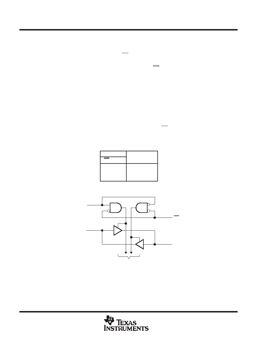
FUNCTION TABLE
(each 8-bit section)
INPUTS
OPERATION
OE
DIR
OPERATION
L
L
B data to A bus
L
H
A data to B bus
H
X
All outputs Hi-Z
logic diagram (positive logic)
DIR
OE
A1
B1
To Seven Other Channels
2
3
22
21

SN74AVCH8T245
8 BIT DUAL SUPPLY BUS TRANSCEIVER
WITH CONFIGURABLE VOLTAGE TRANSLATION AND 3 STATE OUTPUTS
SCES565F - APRIL 2004 - REVISED APRIL 2005
3
POST OFFICE BOX 655303
∑
DALLAS, TEXAS 75265
absolute maximum ratings over operating free-air temperature range (unless otherwise noted)
Supply voltage range, V
CCA
and V
CCB
-0.5 V to 4.6 V
. . . . . . . . . . . . . . . . . . . . . . . . . . . . . . . . . . . . . . . . . . . . . .
Input voltage range, V
I
(see Note 1): I/O ports (A port)
-0.5 V to 4.6 V
. . . . . . . . . . . . . . . . . . . . . . . . . . . . . . . . .
I/O ports (B port)
-0.5 V to 4.6 V
. . . . . . . . . . . . . . . . . . . . . . . . . . . . . . . . .
Control inputs
-0.5 V to 4.6 V
. . . . . . . . . . . . . . . . . . . . . . . . . . . . . . . . . . .
Voltage range applied to any output in the high-impedance or power-off state, V
O
(see Note 1): A port
-0.5 V to 4.6 V
. . . . . . . . . . . . . . . . . . . . . . . . . . . . . . . . . . . . . . . . . . . . . . . . . . . . . . . . . . . .
B port
-0.5 V to 4.6 V
. . . . . . . . . . . . . . . . . . . . . . . . . . . . . . . . . . . . . . . . . . . . . . . . . . . . . . . . . . . .
Voltage range applied to any output in the high or low state, V
O
(see Notes 1 and 2): A port
-0.5 V to V
CCA
+ 0.5 V
. . . . . . . . . . . . . . . . . . . . . . . . . . . . . . . . . . . . . . . . . . . . . .
B port
-0.5 V to V
CCB
+ 0.5 V
. . . . . . . . . . . . . . . . . . . . . . . . . . . . . . . . . . . . . . . . . . . . . .
Input clamp current, I
IK
(V
I
< 0)
-50 mA
. . . . . . . . . . . . . . . . . . . . . . . . . . . . . . . . . . . . . . . . . . . . . . . . . . . . . . . . . . .
Output clamp current, I
OK
(V
O
< 0)
-50 mA
. . . . . . . . . . . . . . . . . . . . . . . . . . . . . . . . . . . . . . . . . . . . . . . . . . . . . . . .
Continuous output current, I
O
±
50 mA
. . . . . . . . . . . . . . . . . . . . . . . . . . . . . . . . . . . . . . . . . . . . . . . . . . . . . . . . . . . . .
Continuous current through V
CCA
, V
CCB
, or GND
±
100 mA
. . . . . . . . . . . . . . . . . . . . . . . . . . . . . . . . . . . . . . . . .
Package thermal impedance,
JA
(see Note 3): DGV package
86
∞
C/W
. . . . . . . . . . . . . . . . . . . . . . . . . . . . . . . .
PW package
88
∞
C/W
. . . . . . . . . . . . . . . . . . . . . . . . . . . . . . . . .
RHL package
43
∞
C/W
. . . . . . . . . . . . . . . . . . . . . . . . . . . . . . . .
Storage temperature range, T
stg
-65
∞
C to 150
∞
C
. . . . . . . . . . . . . . . . . . . . . . . . . . . . . . . . . . . . . . . . . . . . . . . . . . .
Stresses beyond those listed under "absolute maximum ratings" may cause permanent damage to the device. These are stress ratings only, and
functional operation of the device at these or any other conditions beyond those indicated under "recommended operating conditions" is not
implied. Exposure to absolute-maximum-rated conditions for extended periods may affect device reliability.
NOTES:
1. The input voltage and output negative-voltage ratings may be exceeded if the input and output current ratings are observed.
2. The output positive-voltage rating may be exceeded up to 4.6 V maximum if the output current rating is observed.
3. The package thermal impedance is calculated in accordance with JESD 51-7.

SN74AVCH8T245
8 BIT DUAL SUPPLY BUS TRANSCEIVER
WITH CONFIGURABLE VOLTAGE TRANSLATION AND 3 STATE OUTPUTS
SCES565F - APRIL 2004 - REVISED APRIL 2005
4
POST OFFICE BOX 655303
∑
DALLAS, TEXAS 75265
recommended operating conditions (see Notes 4 through 6)
VCCI
VCCO
MIN
MAX
UNIT
VCCA
Supply voltage
1.2
3.6
V
VCCB
Supply voltage
1.2
3.6
V
High-level
1.2 V to 1.95 V
VCCI
◊
0.65
VIH
High-level
input voltage
Data inputs
1.95 V to 2.7 V
1.6
V
VIH
input voltage
Data inputs
2.7 V to 3.6 V
2
V
Low-level
1.2 V to 1.95 V
VCCI
◊
0.35
VIL
Low-level
input voltage
Data inputs
1.95 V to 2.7 V
0.7
V
VIL
input voltage
Data inputs
2.7 V to 3.6 V
0.8
V
High-level
DIR
1.2 V to 1.95 V
VCCA
◊
0.65
VIH
High-level
input voltage
DIR
(referenced to VCCA)
1.95 V to 2.7 V
1.6
V
VIH
input voltage
(referenced to VCCA)
2.7 V to 3.6 V
2
V
Low-level
DIR
1.2 V to 1.95 V
VCCA
◊
0.35
VIL
Low-level
input voltage
DIR
(referenced to VCCA)
1.95 V to 2.7 V
0.7
V
VIL
input voltage
(referenced to VCCA)
2.7 V to 3.6 V
0.8
V
VI
Input voltage
0
3.6
V
VO
Output voltage
Active state
0
VCCO
V
VO
Output voltage
3-state
0
3.6
V
1.2 V
-3
1.4 V to 1.6 V
-6
IOH
High-level output current
1.65 V to 1.95 V
-8
mA
IOH
High-level output current
2.3 V to 2.7 V
-9
mA
3 V to 3.6 V
-12
1.2 V
3
1.4 V to 1.6 V
6
IOL
Low-level output current
1.65 V to 1.95 V
8
mA
IOL
Low-level output current
2.3 V to 2.7 V
9
mA
3 V to 3.6 V
12
t/
v
Input transition rise or fall rate
5
ns/V
TA
Operating free-air temperature
-40
85
∞
C
NOTES:
4. VCCI is the VCC associated with the data input port.
5. VCCO is the VCC associated with the output port.
6. All unused data inputs of the device must be held at VCCI or GND to ensure proper device operation. Refer to the TI application report,
Implications of Slow or Floating CMOS Inputs, literature number SCBA004.

SN74AVCH8T245
8 BIT DUAL SUPPLY BUS TRANSCEIVER
WITH CONFIGURABLE VOLTAGE TRANSLATION AND 3 STATE OUTPUTS
SCES565F - APRIL 2004 - REVISED APRIL 2005
5
POST OFFICE BOX 655303
∑
DALLAS, TEXAS 75265
electrical characteristics over recommended operating free-air temperature range (unless
otherwise noted) (see Note 7)
PARAMETER
TEST CONDITIONS
VCCA
VCCB
TA = 25
∞
C
-40
∞
C to 85
∞
C
UNIT
PARAMETER
TEST CONDITIONS
VCCA
VCCB
MIN
TYP
MAX
MIN
MAX
UNIT
IOH = -100
µ
A
1.2 V to 3.6 V
1.2 V to 3.6 V
VCCO - 0.2 V
IOH = -3 mA
1.2 V
1.2 V
0.95
VOH
IOH = -6 mA
VI = VIH
1.4 V
1.4 V
1.05
V
VOH
IOH = -8 mA
VI = VIH
1.65 V
1.65 V
1.2
V
IOH = -9 mA
2.3 V
2.3 V
1.75
IOH = -12 mA
3 V
3 V
2.3
IOL = 100
µ
A
1.2 V to 3.6 V
1.2 V to 3.6 V
0.2
IOL = 3 mA
1.2 V
1.2 V
0.15
VOL
IOL = 6 mA
VI = VIL
1.4 V
1.4 V
0.35
V
VOL
IOL = 8 mA
VI = VIL
1.65 V
1.65 V
0.45
V
IOL = 9 mA
2.3 V
2.3 V
0.55
IOL = 12 mA
3 V
3 V
0.7
II
Control
inputs
VI = VCCA or GND
1.2 V to 3.6 V
1.2 V to 3.6 V
±
0.025
±
0.25
±
1
µ
A
VI = 0.42 V
1.2 V
1.2 V
25
VI = 0.49 V
1.4 V
1.4 V
15
IBHL
VI = 0.58 V
1.65 V
1.65 V
25
µ
A
IBHL
VI = 0.7 V
2.3 V
2.3 V
45
µ
A
VI = 0.8 V
3.3 V
3.3 V
100
VI = 0.78 V
1.2 V
1.2 V
-25
VI = 0.91 V
1.4 V
1.4 V
-15
IBHH
VI = 1.07 V
1.65 V
1.65 V
-25
µ
A
IBHH
VI = 1.6 V
2.3 V
2.3 V
-45
µ
A
VI = 2 V
3.3 V
3.3 V
-100
1.2 V
1.2 V
50
1.6 V
1.6 V
125
IBHLOß
VI = 0 to VCC
1.95 V
1.95 V
200
µ
A
IBHLOß
VI = 0 to VCC
2.7 V
2.7 V
300
µ
A
3.6 V
3.6 V
500
1.2 V
1.2 V
-50
1.6 V
1.6 V
-125
IBHHO∂
VI = 0 to VCC
1.95 V
1.95 V
-200
µ
A
IBHHO∂
VI = 0 to VCC
2.7 V
2.7 V
-300
µ
A
3.6 V
3.6 V
-500
The bus-hold circuit can sink at least the minimum low sustaining current at VIL max. IBHL should be measured after lowering VIN to GND and
then raising it to VIL max.
The bus-hold circuit can source at least the minimum high sustaining current at VIH min. IBHH should be measured after raising VIN to VCC and
then lowering it to VIH min.
ß An external driver must source at least IBHLO to switch this node from low to high.
∂ An external driver must sink at least IBHHO to switch this node from high to low.
NOTE 7: VCCO is the VCC associated with the output port.

SN74AVCH8T245
8 BIT DUAL SUPPLY BUS TRANSCEIVER
WITH CONFIGURABLE VOLTAGE TRANSLATION AND 3 STATE OUTPUTS
SCES565F - APRIL 2004 - REVISED APRIL 2005
6
POST OFFICE BOX 655303
∑
DALLAS, TEXAS 75265
electrical characteristics over recommended operating free-air temperature range (unless
otherwise noted) (see Notes 8 and 9) (continued)
PARAMETER
TEST CONDITIONS
VCCA
VCCB
TA = 25
∞
C
-40
∞
C to 85
∞
C
UNIT
PARAMETER
TEST CONDITIONS
VCCA
VCCB
MIN
TYP
MAX
MIN
MAX
UNIT
Ioff
A port
VI or VO = 0 to 3.6 V
0 V
0 to 3.6 V
±
0.1
±
1
±
5
A
Ioff
B port
VI or VO = 0 to 3.6 V
0 to 3.6 V
0 V
±
0.1
±
1
±
5
µ
A
I
A or B
port
VO = VCCO or GND,
VI = VCCI or GND
OE = VIH
3.6 V
3.6 V
±
0.5
±
2.5
±
5
µ
A
IOZ
B port
VO = VCCO or GND, OE = don't
0 V
3.6 V
±
5
µ
A
A port
VO = VCCO or GND,
VI = VCCI or GND
OE = don't
care
3.6 V
0 V
±
5
µ
A
1.2 V to 3.6 V
1.2 V to 3.6 V
15
ICCA
VI = VCCI or GND
IO = 0
0 V
3.6 V
-2
µ
A
ICCA
VI = VCCI or GND
IO = 0
3.6 V
0 V
15
µ
A
1.2 V to 3.6 V
1.2 V to 3.6 V
15
ICCB
VI = VCCI or GND
IO = 0
0 V
3.6 V
15
µ
A
ICCB
VI = VCCI or GND
IO = 0
3.6 V
0 V
-2
µ
A
ICCA + ICCB
VI = VCCI or GND
IO = 0
1.2 V to 3.6 V
1.2 V to 3.6 V
25
µ
A
Ci
Control
inputs
VI = 3.3 V or GND
3.3 V
3.3 V
3.5
4.5
pF
Cio
A or B
port
VO = 3.3 V or GND
3.3 V
3.3 V
6
7
pF
For I/O ports, the parameter IOZ includes the input leakage current.
NOTES:
8. VCCO is the VCC associated with the output port.
9. VCCI is the VCC associated with the input port.
switching characteristics over recommended operating free-air temperature range,
V
CCA
= 1.2 V (see Figure 10)
PARAMETER
FROM
TO
VCCB = 1.2 V
VCCB = 1.5 V
VCCB = 1.8 V
VCCB = 2.5 V
VCCB = 3.3 V
UNIT
PARAMETER
FROM
(INPUT)
TO
(OUTPUT)
TYP
TYP
TYP
TYP
TYP
UNIT
tPLH
A
B
3.1
2.6
2.5
3
3.5
ns
tPHL
A
B
3.1
2.6
2.5
3
3.5
ns
tPLH
B
A
3.1
2.7
2.5
2.4
2.3
ns
tPHL
B
A
3.1
2.7
2.5
2.4
2.3
ns
tPZH
OE
A
5.3
5.3
5.3
5.3
5.3
ns
tPZL
OE
A
5.3
5.3
5.3
5.3
5.3
ns
tPZH
OE
B
5.1
4
3.5
3.2
3.1
ns
tPZL
OE
B
5.1
4
3.5
3.2
3.1
ns
tPHZ
OE
A
4.8
4.8
4.8
4.8
4.8
ns
tPLZ
OE
A
4.8
4.8
4.8
4.8
4.8
ns
tPHZ
OE
B
4.7
4
4.1
4.3
5.1
ns
tPLZ
OE
B
4.7
4
4.1
4.3
5.1
ns

SN74AVCH8T245
8 BIT DUAL SUPPLY BUS TRANSCEIVER
WITH CONFIGURABLE VOLTAGE TRANSLATION AND 3 STATE OUTPUTS
SCES565F - APRIL 2004 - REVISED APRIL 2005
7
POST OFFICE BOX 655303
∑
DALLAS, TEXAS 75265
switching characteristics over recommended operating free-air temperature range,
V
CCA
= 1.5 V
±
0.1 V (see Figure 10)
PARAMETER
FROM
(INPUT)
TO
(OUTPUT)
VCCB = 1.2 V
VCCB = 1.5 V
±
0.1 V
VCCB = 1.8 V
±
0.15 V
VCCB = 2.5 V
±
0.2 V
VCCB = 3.3 V
±
0.3 V
UNIT
PARAMETER
(INPUT)
(OUTPUT)
TYP
MIN
MAX
MIN
MAX
MIN
MAX
MIN
MAX
UNIT
tPLH
A
B
2.7
0.5
5.4
0.5
4.6
0.5
4.9
0.5
6.8
ns
tPHL
A
B
2.7
0.5
5.4
0.5
4.6
0.5
4.9
0.5
6.8
ns
tPLH
B
A
2.6
0.5
5.4
0.5
5.1
0.5
4.7
0.5
4.5
ns
tPHL
B
A
2.6
0.5
5.4
0.5
5.1
0.5
4.7
0.5
4.5
ns
tPZH
OE
A
3.7
1.1
8.7
1.1
8.7
1.1
8.7
1.1
8.7
ns
tPZL
OE
A
3.7
1.1
8.7
1.1
8.7
1.1
8.7
1.1
8.7
ns
tPZH
OE
B
4.8
1.1
7.6
1.1
7.1
1
5.6
1
5.2
ns
tPZL
OE
B
4.8
1.1
7.6
1.1
7.1
1
5.6
1
5.2
ns
tPHZ
OE
A
3.1
0.5
8.6
0.5
8.6
0.5
8.6
0.5
8.6
ns
tPLZ
OE
A
3.1
0.5
8.6
0.5
8.6
0.5
8.6
0.5
8.6
ns
tPHZ
OE
B
4.1
0.5
8.4
0.5
7.6
0.5
7.2
0.5
7.8
ns
tPLZ
OE
B
4.1
0.5
8.4
0.5
7.6
0.5
7.2
0.5
7.8
ns
switching characteristics over recommended operating free-air temperature range,
V
CCA
= 1.8 V
±
0.15 V (see Figure 10)
PARAMETER
FROM
(INPUT)
TO
(OUTPUT)
VCCB = 1.2 V
VCCB = 1.5 V
±
0.1 V
VCCB = 1.8 V
±
0.15 V
VCCB = 2.5 V
±
0.2 V
VCCB = 3.3 V
±
0.3 V
UNIT
PARAMETER
(INPUT)
(OUTPUT)
TYP
MIN
MAX
MIN
MAX
MIN
MAX
MIN
MAX
UNIT
tPLH
A
B
2.5
0.5
5.1
0.5
4.4
0.5
4
0.5
3.9
ns
tPHL
A
B
2.5
0.5
5.1
0.5
4.4
0.5
4
0.5
3.9
ns
tPLH
B
A
2.5
0.5
4.6
0.5
4.4
0.5
3.9
0.5
3.7
ns
tPHL
B
A
2.5
0.5
4.6
0.5
4.4
0.5
3.9
0.5
3.7
ns
tPZH
OE
A
3
1
6.8
1
6.8
1
6.8
1
6.8
ns
tPZL
OE
A
3
1
6.8
1
6.8
1
6.8
1
6.8
ns
tPZH
OE
B
4.6
1.1
8.2
1
6.7
0.5
5.1
0.5
4.5
ns
tPZL
OE
B
4.6
1.1
8.2
1
6.7
0.5
5.1
0.5
4.5
ns
tPHZ
OE
A
2.8
0.5
7.1
0.5
7.1
0.5
7.1
0.5
7.1
ns
tPLZ
OE
A
2.8
0.5
7.1
0.5
7.1
0.5
7.1
0.5
7.1
ns
tPHZ
OE
B
3.9
0.5
7.8
0.5
6.9
0.5
6
0.5
5.8
ns
tPLZ
OE
B
3.9
0.5
7.8
0.5
6.9
0.5
6
0.5
5.8
ns

SN74AVCH8T245
8 BIT DUAL SUPPLY BUS TRANSCEIVER
WITH CONFIGURABLE VOLTAGE TRANSLATION AND 3 STATE OUTPUTS
SCES565F - APRIL 2004 - REVISED APRIL 2005
8
POST OFFICE BOX 655303
∑
DALLAS, TEXAS 75265
switching characteristics over recommended operating free-air temperature range,
V
CCA
= 2.5 V
±
0.2 V (see Figure 10)
PARAMETER
FROM
(INPUT)
TO
(OUTPUT)
VCCB = 1.2 V
VCCB = 1.5 V
±
0.1 V
VCCB = 1.8 V
±
0.15 V
VCCB = 2.5 V
±
0.2 V
VCCB = 3.3 V
±
0.3 V
UNIT
PARAMETER
(INPUT)
(OUTPUT)
TYP
MIN
MAX
MIN
MAX
MIN
MAX
MIN
MAX
UNIT
tPLH
A
B
2.4
0.5
4.7
0.5
3.9
0.5
3.1
0.5
2.8
ns
tPHL
A
B
2.4
0.5
4.7
0.5
3.9
0.5
3.1
0.5
2.8
ns
tPLH
B
A
3
0.5
4.9
0.5
4
0.5
3.1
0.5
2.9
ns
tPHL
B
A
3
0.5
4.9
0.5
4
0.5
3.1
0.5
2.9
ns
tPZH
OE
A
2.2
0.5
4.8
0.5
4.8
0.5
4.8
0.5
4.8
ns
tPZL
OE
A
2.2
0.5
4.8
0.5
4.8
0.5
4.8
0.5
4.8
ns
tPZH
OE
B
4.5
1.1
7.9
0.5
6.4
0.5
4.6
0.5
4
ns
tPZL
OE
B
4.5
1.1
7.9
0.5
6.4
0.5
4.6
0.5
4
ns
tPHZ
OE
A
1.8
0.5
5.1
0.5
5.1
0.5
5.1
0.5
5.1
ns
tPLZ
OE
A
1.8
0.5
5.1
0.5
5.1
0.5
5.1
0.5
5.1
ns
tPHZ
OE
B
3.6
0.5
7.1
0.5
6.3
0.5
5.1
0.5
3.9
ns
tPLZ
OE
B
3.6
0.5
7.1
0.5
6.3
0.5
5.1
0.5
3.9
ns
switching characteristics over recommended operating free-air temperature range,
V
CCA
= 3.3 V
±
0.3 V (see Figure 10)
PARAMETER
FROM
(INPUT)
TO
(OUTPUT)
VCCB = 1.2 V
VCCB = 1.5 V
±
0.1 V
VCCB = 1.8 V
±
0.15 V
VCCB = 2.5 V
±
0.2 V
VCCB = 3.3 V
±
0.3 V
UNIT
PARAMETER
(INPUT)
(OUTPUT)
TYP
MIN
MAX
MIN
MAX
MIN
MAX
MIN
MAX
UNIT
tPLH
A
B
2.3
0.5
4.5
0.5
3.7
0.5
2.9
0.5
2.5
ns
tPHL
A
B
2.3
0.5
4.5
0.5
3.7
0.5
2.9
0.5
2.5
ns
tPLH
B
A
3.5
0.5
6.8
0.5
3.9
0.5
2.8
0.5
2.5
ns
tPHL
B
A
3.5
0.5
6.8
0.5
3.9
0.5
2.8
0.5
2.5
ns
tPZH
OE
A
2
0.5
4
0.5
4
0.5
4
0.5
4
ns
tPZL
OE
A
2
0.5
4
0.5
4
0.5
4
0.5
4
ns
tPZH
OE
B
4.5
1.1
7.8
0.5
6.2
0.5
4.5
0.5
3.9
ns
tPZL
OE
B
4.5
1.1
7.8
0.5
6.2
0.5
4.5
0.5
3.9
ns
tPHZ
OE
A
1.7
0.5
4
0.5
4
0.5
4
0.5
4
ns
tPLZ
OE
A
1.7
0.5
4
0.5
4
0.5
4
0.5
4
ns
tPHZ
OE
B
3.4
0.5
6.9
0.5
6
0.5
4.8
0.5
4.2
ns
tPLZ
OE
B
3.4
0.5
6.9
0.5
6
0.5
4.8
0.5
4.2
ns

SN74AVCH8T245
8 BIT DUAL SUPPLY BUS TRANSCEIVER
WITH CONFIGURABLE VOLTAGE TRANSLATION AND 3 STATE OUTPUTS
SCES565F - APRIL 2004 - REVISED APRIL 2005
9
POST OFFICE BOX 655303
∑
DALLAS, TEXAS 75265
operating characteristics, T
A
= 25
∞
C
PARAMETER
TEST
CONDITIONS
VCCA =
VCCB = 1.2 V
VCCA =
VCCB = 1.5 V
VCCA =
VCCB = 1.8 V
VCCA =
VCCB = 2.5 V
VCCA =
VCCB = 3.3 V
UNIT
PARAMETER
CONDITIONS
TYP
TYP
TYP
TYP
TYP
UNIT
A to B
Outputs
enabled
1
1
1
1
1
CpdA
A to B
Outputs
disabled
CL = 0,
f = 10 MHz,
1
1
1
1
1
pF
CpdA
B to A
Outputs
enabled
f = 10 MHz,
tr = tf =1 ns
12
12
12
13
14
pF
B to A
Outputs
disabled
1
1
1
1
1
A to B
Outputs
enabled
12
12
12
13
14
CpdB
A to B
Outputs
disabled
CL = 0,
f = 10 MHz,
1
1
1
1
1
pF
CpdB
B to A
Outputs
enabled
f = 10 MHz,
tr = tf =1 ns
1
1
1
1
1
pF
B to A
Outputs
disabled
1
1
1
1
1
Power-dissipation capacitance per transceiver
typical total static power consumption (I
CCA
+ I
CCB
)
Table 1
VCCB
VCCA
UNIT
VCCB
0 V
1.2 V
1.5 V
1.8 V
2.5 V
3.3 V
UNIT
0 V
0
<
0.5
<
0.5
<
0.5
<
0.5
<
0.5
1.2 V
<
0.5
<
1
<
1
<
1
<
1
1
1.5 V
<
0.5
<
1
<
1
<
1
<
1
1
A
1.8 V
<
0.5
<
1
<
1
<
1
<
1
<
1
µ
A
2.5 V
<
0.5
1
<
1
<
1
<
1
<
1
3.3 V
<
0.5
1
<
1
<
1
<
1
<
1

SN74AVCH8T245
8 BIT DUAL SUPPLY BUS TRANSCEIVER
WITH CONFIGURABLE VOLTAGE TRANSLATION AND 3 STATE OUTPUTS
SCES565F - APRIL 2004 - REVISED APRIL 2005
10
POST OFFICE BOX 655303
∑
DALLAS, TEXAS 75265
TYPICAL CHARACTERISTICS
TYPICAL PROPAGATION DELAY (A to B) vs LOAD CAPACITANCE
T
A
= 25
∞
C, V
CCA
= 1.2 V
0
1
2
3
4
5
6
0
10
20
30
40
50
Figure 1
t PD
- ns
CL - pF
60
VCCB = 1.8 V
VCCB = 2.5 V
VCCB = 3.3 V
VCCB = 1.5 V
VCCB = 1.2 V
TYPICAL PROPAGATION DELAY (A to B) vs LOAD CAPACITANCE
T
A
= 25
∞
C, V
CCA
= 1.5 V
Figure 2
CL - pF
0
1
2
3
4
5
6
VCCB = 1.8 V
VCCB = 2.5 V
VCCB = 3.3 V
VCCB = 1.5 V
VCCB = 1.2 V
0
10
20
30
40
50
60
t PLH
- ns
Figure 3
0
1
2
3
4
5
6
0
10
20
30
40
50
60
t PHL
- ns
CL - pF
VCCB = 1.8 V
VCCB = 2.5 V
VCCB = 3.3 V
VCCB = 1.5 V
VCCB = 1.2 V

SN74AVCH8T245
8 BIT DUAL SUPPLY BUS TRANSCEIVER
WITH CONFIGURABLE VOLTAGE TRANSLATION AND 3 STATE OUTPUTS
SCES565F - APRIL 2004 - REVISED APRIL 2005
11
POST OFFICE BOX 655303
∑
DALLAS, TEXAS 75265
TYPICAL PROPAGATION DELAY (A to B) vs LOAD CAPACITANCE
T
A
= 25
∞
C, V
CCA
= 1.8 V
Figure 4
CL - pF
t PLH
- ns
0
10
20
30
40
50
60
0
1
2
3
4
5
6
VCCB = 1.8 V
VCCB = 2.5 V
VCCB = 3.3 V
VCCB = 1.5 V
VCCB = 1.2 V
Figure 5
0
1
2
3
4
5
6
0
10
20
30
40
50
60
VCCB = 1.8 V
VCCB = 2.5 V
VCCB = 3.3 V
VCCB = 1.5 V
VCCB = 1.2 V
t PHL
- ns
CL - pF
TYPICAL PROPAGATION DELAY (A to B) vs LOAD CAPACITANCE
T
A
= 25
∞
C, V
CCA
= 2.5 V
Figure 6
CL - pF
t PLH
- ns
VCCB = 1.8 V
VCCB = 2.5 V
VCCB = 3.3 V
VCCB = 1.5 V
VCCB = 1.2 V
0
1
2
3
4
5
6
0
10
20
30
40
50
60
Figure 7
0
1
2
3
4
5
6
0
10
20
30
40
50
60
VCCB = 1.8 V
VCCB = 2.5 V
VCCB = 3.3 V
VCCB = 1.5 V
VCCB = 1.2 V
CL - pF
t PHL
- ns

SN74AVCH8T245
8 BIT DUAL SUPPLY BUS TRANSCEIVER
WITH CONFIGURABLE VOLTAGE TRANSLATION AND 3 STATE OUTPUTS
SCES565F - APRIL 2004 - REVISED APRIL 2005
12
POST OFFICE BOX 655303
∑
DALLAS, TEXAS 75265
TYPICAL PROPAGATION DELAY (A to B) vs LOAD CAPACITANCE
T
A
= 25
∞
C, V
CCA
= 3.3 V
Figure 8
t PLH
- ns
0
1
2
3
4
5
6
VCCB = 1.8 V
VCCB = 2.5 V
VCCB = 3.3 V
VCCB = 1.5 V
VCCB = 1.2 V
CL - pF
0
10
20
30
40
50
60
Figure 9
0
1
2
3
4
5
6
0
10
20
30
40
50
60
VCCB = 1.8 V
VCCB = 2.5 V
VCCB = 3.3 V
VCCB = 1.5 V
VCCB = 1.2 V
CL - pF
t PHL
- ns

SN74AVCH8T245
8 BIT DUAL SUPPLY BUS TRANSCEIVER
WITH CONFIGURABLE VOLTAGE TRANSLATION AND 3 STATE OUTPUTS
SCES565F - APRIL 2004 - REVISED APRIL 2005
13
POST OFFICE BOX 655303
∑
DALLAS, TEXAS 75265
PARAMETER MEASUREMENT INFORMATION
VOH
VOL
From Output
Under Test
CL
(see Note A)
LOAD CIRCUIT
S1
2
◊
VCCO
Open
GND
RL
RL
tPLH
tPHL
Output
Control
(low-level
enabling)
Output
Waveform 1
S1 at 2
◊
VCCO
(see Note B)
Output
Waveform 2
S1 at GND
(see Note B)
tPZL
tPZH
tPLZ
tPHZ
VCCA/2
VCCA/2
VCCI/2
VCCI/2
VCCI
0 V
VCCO/2
VCCO/2
VOH
VOL
0 V
VCCO/2
VOL + VTP
VCCO/2
VOH - VTP
0 V
VCCI
0 V
VCCI/2
VCCI/2
tw
Input
VCCA
VCCO
VOLTAGE WAVEFORMS
PROPAGATION DELAY TIMES
VOLTAGE WAVEFORMS
PULSE DURATION
VOLTAGE WAVEFORMS
ENABLE AND DISABLE TIMES
Output
Input
tpd
tPLZ/tPZL
tPHZ/tPZH
Open
2
◊
VCCO
GND
TEST
S1
NOTES: A. CL includes probe and jig capacitance.
B. Waveform 1 is for an output with internal conditions such that the output is low, except when disabled by the output control.
Waveform 2 is for an output with internal conditions such that the output is high, except when disabled by the output control.
C. All input pulses are supplied by generators having the following characteristics: PRR
v
10 MHz, ZO = 50
, dv/dt
1 V/ns.
D. The outputs are measured one at a time, with one transition per measurement.
E. tPLZ and tPHZ are the same as tdis.
F. tPZL and tPZH are the same as ten.
G. tPLH and tPHL are the same as tpd.
H. VCCI is the VCC associated with the input port.
I. VCCO is the VCC associated with the output port.
1.2 V
1.5 V
±
0.1 V
1.8 V
±
0.15 V
2.5 V
±
0.2 V
3.3 V
±
0.3 V
2 k
2 k
2 k
2 k
2 k
VCCO
RL
0.1 V
0.1 V
0.15 V
0.15 V
0.3 V
VTP
CL
15 pF
15 pF
15 pF
15 pF
15 pF
Figure 10. Load Circuit and Voltage Waveforms

SN74AVCH8T245
8 BIT DUAL SUPPLY BUS TRANSCEIVER
WITH CONFIGURABLE VOLTAGE TRANSLATION AND 3 STATE OUTPUTS
SCES565F - APRIL 2004 - REVISED APRIL 2005
14
POST OFFICE BOX 655303
∑
DALLAS, TEXAS 75265

PACKAGING INFORMATION
Orderable Device
Status
(1)
Package
Type
Package
Drawing
Pins Package
Qty
Eco Plan
(2)
Lead/Ball Finish
MSL Peak Temp
(3)
74AVCH8T245DGVRE4
ACTIVE
TVSOP
DGV
24
2000 Green (RoHS &
no Sb/Br)
CU NIPDAU
Level-1-260C-UNLIM
74AVCH8T245PWRE4
ACTIVE
TSSOP
PW
24
2000 Green (RoHS &
no Sb/Br)
CU NIPDAU
Level-1-260C-UNLIM
SN74AVCH8T245DGVR
ACTIVE
TVSOP
DGV
24
2000 Green (RoHS &
no Sb/Br)
CU NIPDAU
Level-1-260C-UNLIM
SN74AVCH8T245PW
ACTIVE
TSSOP
PW
24
60
Green (RoHS &
no Sb/Br)
CU NIPDAU
Level-1-260C-UNLIM
SN74AVCH8T245PWE4
ACTIVE
TSSOP
PW
24
60
Green (RoHS &
no Sb/Br)
CU NIPDAU
Level-1-260C-UNLIM
SN74AVCH8T245PWR
ACTIVE
TSSOP
PW
24
2000 Green (RoHS &
no Sb/Br)
CU NIPDAU
Level-1-260C-UNLIM
SN74AVCH8T245RHLR
ACTIVE
QFN
RHL
24
1000 Green (RoHS &
no Sb/Br)
CU NIPDAU
Level-2-260C-1YEAR
(1)
The marketing status values are defined as follows:
ACTIVE: Product device recommended for new designs.
LIFEBUY: TI has announced that the device will be discontinued, and a lifetime-buy period is in effect.
NRND: Not recommended for new designs. Device is in production to support existing customers, but TI does not recommend using this part in
a new design.
PREVIEW: Device has been announced but is not in production. Samples may or may not be available.
OBSOLETE: TI has discontinued the production of the device.
(2)
Eco
Plan
-
The
planned
eco-friendly
classification:
Pb-Free
(RoHS)
or
Green
(RoHS
&
no
Sb/Br)
-
please
check
http://www.ti.com/productcontent
for the latest availability information and additional product content details.
TBD: The Pb-Free/Green conversion plan has not been defined.
Pb-Free (RoHS): TI's terms "Lead-Free" or "Pb-Free" mean semiconductor products that are compatible with the current RoHS requirements
for all 6 substances, including the requirement that lead not exceed 0.1% by weight in homogeneous materials. Where designed to be soldered
at high temperatures, TI Pb-Free products are suitable for use in specified lead-free processes.
Green (RoHS & no Sb/Br): TI defines "Green" to mean Pb-Free (RoHS compatible), and free of Bromine (Br) and Antimony (Sb) based flame
retardants (Br or Sb do not exceed 0.1% by weight in homogeneous material)
(3)
MSL, Peak Temp. -- The Moisture Sensitivity Level rating according to the JEDEC industry standard classifications, and peak solder
temperature.
Important Information and Disclaimer:The information provided on this page represents TI's knowledge and belief as of the date that it is
provided. TI bases its knowledge and belief on information provided by third parties, and makes no representation or warranty as to the
accuracy of such information. Efforts are underway to better integrate information from third parties. TI has taken and continues to take
reasonable steps to provide representative and accurate information but may not have conducted destructive testing or chemical analysis on
incoming materials and chemicals. TI and TI suppliers consider certain information to be proprietary, and thus CAS numbers and other limited
information may not be available for release.
In no event shall TI's liability arising out of such information exceed the total purchase price of the TI part(s) at issue in this document sold by TI
to Customer on an annual basis.
PACKAGE OPTION ADDENDUM
www.ti.com
9-Aug-2005
Addendum-Page 1

MECHANICAL DATA
MPDS006C ≠ FEBRUARY 1996 ≠ REVISED AUGUST 2000
POST OFFICE BOX 655303
∑
DALLAS, TEXAS 75265
DGV (R-PDSO-G**)
PLASTIC SMALL-OUTLINE
24 PINS SHOWN
14
3,70
3,50
4,90
5,10
20
DIM
PINS **
4073251/E 08/00
1,20 MAX
Seating Plane
0,05
0,15
0,25
0,50
0,75
0,23
0,13
1
12
24
13
4,30
4,50
0,16 NOM
Gage Plane
A
7,90
7,70
38
24
16
4,90
5,10
3,70
3,50
A MAX
A MIN
6,60
6,20
11,20
11,40
56
9,60
9,80
48
0,08
M
0,07
0,40
0
∞
≠ 8
∞
NOTES: A. All linear dimensions are in millimeters.
B. This drawing is subject to change without notice.
C. Body dimensions do not include mold flash or protrusion, not to exceed 0,15 per side.
D. Falls within JEDEC: 24/48 Pins ≠ MO-153
14/16/20/56 Pins ≠ MO-194

MECHANICAL DATA
MTSS001C ≠ JANUARY 1995 ≠ REVISED FEBRUARY 1999
POST OFFICE BOX 655303
∑
DALLAS, TEXAS 75265
PW (R-PDSO-G**)
PLASTIC SMALL-OUTLINE PACKAGE
14 PINS SHOWN
0,65
M
0,10
0,10
0,25
0,50
0,75
0,15 NOM
Gage Plane
28
9,80
9,60
24
7,90
7,70
20
16
6,60
6,40
4040064/F 01/97
0,30
6,60
6,20
8
0,19
4,30
4,50
7
0,15
14
A
1
1,20 MAX
14
5,10
4,90
8
3,10
2,90
A MAX
A MIN
DIM
PINS **
0,05
4,90
5,10
Seating Plane
0
∞
≠ 8
∞
NOTES: A. All linear dimensions are in millimeters.
B. This drawing is subject to change without notice.
C. Body dimensions do not include mold flash or protrusion not to exceed 0,15.
D. Falls within JEDEC MO-153

IMPORTANT NOTICE
Texas Instruments Incorporated and its subsidiaries (TI) reserve the right to make corrections, modifications,
enhancements, improvements, and other changes to its products and services at any time and to discontinue
any product or service without notice. Customers should obtain the latest relevant information before placing
orders and should verify that such information is current and complete. All products are sold subject to TI's terms
and conditions of sale supplied at the time of order acknowledgment.
TI warrants performance of its hardware products to the specifications applicable at the time of sale in
accordance with TI's standard warranty. Testing and other quality control techniques are used to the extent TI
deems necessary to support this warranty. Except where mandated by government requirements, testing of all
parameters of each product is not necessarily performed.
TI assumes no liability for applications assistance or customer product design. Customers are responsible for
their products and applications using TI components. To minimize the risks associated with customer products
and applications, customers should provide adequate design and operating safeguards.
TI does not warrant or represent that any license, either express or implied, is granted under any TI patent right,
copyright, mask work right, or other TI intellectual property right relating to any combination, machine, or process
in which TI products or services are used. Information published by TI regarding third-party products or services
does not constitute a license from TI to use such products or services or a warranty or endorsement thereof.
Use of such information may require a license from a third party under the patents or other intellectual property
of the third party, or a license from TI under the patents or other intellectual property of TI.
Reproduction of information in TI data books or data sheets is permissible only if reproduction is without
alteration and is accompanied by all associated warranties, conditions, limitations, and notices. Reproduction
of this information with alteration is an unfair and deceptive business practice. TI is not responsible or liable for
such altered documentation.
Resale of TI products or services with statements different from or beyond the parameters stated by TI for that
product or service voids all express and any implied warranties for the associated TI product or service and
is an unfair and deceptive business practice. TI is not responsible or liable for any such statements.
Following are URLs where you can obtain information on other Texas Instruments products and application
solutions:
Products
Applications
Amplifiers
amplifier.ti.com
Audio
www.ti.com/audio
Data Converters
dataconverter.ti.com
Automotive
www.ti.com/automotive
DSP
dsp.ti.com
Broadband
www.ti.com/broadband
Interface
interface.ti.com
Digital Control
www.ti.com/digitalcontrol
Logic
logic.ti.com
Military
www.ti.com/military
Power Mgmt
power.ti.com
Optical Networking
www.ti.com/opticalnetwork
Microcontrollers
microcontroller.ti.com
Security
www.ti.com/security
Telephony
www.ti.com/telephony
Video & Imaging
www.ti.com/video
Wireless
www.ti.com/wireless
Mailing Address:
Texas Instruments
Post Office Box 655303 Dallas, Texas 75265
Copyright
2005, Texas Instruments Incorporated