
16-Bit Registers
CY74FCT163374
CY74FCT163H374
SCCS050 - March 1997 - Revised March 2000
Data sheet acquired from Cypress Semiconductor Corporation.
Data sheet modified to remove devices not offered.
Copyright
©
2000, Texas Instruments Incorporated
Features
∑ Low power, pin-compatible replacement for LCX and
LPT families
∑ 5V tolerant inputs and outputs
∑ 24 mA balanced drive outputs
∑ Power-off disable outputs permits live insertion
∑ Edge-rate control circuitry for reduced noise
∑ FCT-C speed at 5.2 ns
∑ Latch-up performance exceeds JEDEC standard no. 17
∑ Typical output skew < 250 ps
∑ Industrial temperature range of ≠40∞C to +85∞C
∑ TSSOP (19.6-mil pitch) or SSOP (25-mil pitch)
∑ Typical Volp (ground bounce) performance exceeds Mil
Std 883D
∑ V
CC
= 2.7V to 3.6V
∑ ESD (HBM) > 2000V
CY74FCT163H374
∑ Bus hold on data inputs
∑ Eliminates the need for external pull-up or pull-down
resistors
∑ Devices with bus hold are not recommended for trans-
lating rail-to-rail CMOS signals to 3.3V logic levels
Functional Description
These devices are 16-bit D-type registers designed for use as
buffered registers in high-speed, low power bus applications.
These devices can be used as two independent 8-bit registers
or as a single 16-bit register by connecting the output Enable
(OE) and Clock (CLK) inputs. The outputs are 24-mA balanced
output drivers with current limiting resistors to reduce the need
for external terminating resistors, and provide for minimal
undershoot and reduced ground bounce. Flow-through pinout
and small shrink packaging aid in simplifying board layout.
The CY74FCT163H374 has "bus hold" on the data inputs,
which retains the input's last state whenever the source driving
the input goes to high impedance. This eliminates the need for
pull-up/down resistors and prevents floating inputs.
The CY74FCT163374 is designed with inputs and outputs
capable of being driven by 5.0V buses, allowing its use in
mixed voltage systems as a translator. The outputs are also
designed with a power off disable feature enabling its use in
applications requiring live insertion.
Lite Drive is a trademark of Cypress Semiconductor Corporation.
Logic Block Diagrams CY74FCT163374, CY74FCT163H374
Pin Configuration
D
C
1
OE
1
CLK
1
D
1
1
O
1
TO 7 OTHER CHANNELS
D
C
2
OE
2
CLK
2
D
1
2
O
1
GND
1
2
3
4
5
6
7
8
9
10
11
12
33
32
31
30
29
25
26
27
28
36
35
1
OE
34
SSOP/TSSOP
Top View
13
14
15
16
17
18
19
20
21
22
23
24
45
44
43
42
41
37
38
39
40
48
47
46
1
O
1
1
O
2
1
O
3
1
O
4
1
D
1
1
D
2
1
D
3
1
D
4
1
CLK
GND
GND
V
CC
1
O
7
1
O
8
1
O
5
1
O
6
1
D
5
1
D
6
1
D
7
1
D
8
V
CC
GND
GND
2
O
3
2
O
4
2
O
1
2
O
2
2
D
1
2
D
2
2
D
3
2
D
4
GND
GND
V
CC
2
O
7
2
O
8
2
O
5
2
O
6
2
D
5
2
D
6
2
D
7
2
D
8
V
CC
GND
2
OE
2
CLK
TO 7 OTHER CHANNELS
CY74FCT163374
CY74FCT163H374
2
Maximum Ratings
[3, 4]
(Above which the useful life may be impaired. For user
guidelines, not tested.)
Storage Temperature
.....................................-
55
∞
C to +125
∞
C
Ambient Temperature with
Power Applied
..................................................-
55
∞
C to +125
∞
C
Supply Voltage Range ..................................... 0.5V to +4.6V
DC Input Voltage
.................................................-
0.5V to +7.0V
DC Output Voltage
..............................................-
0.5V to +7.0V
DC Output Current
(Maximum Sink Current/Pin)
...........................-
60 to +120 mA
Power Dissipation .......................................................... 1.0W
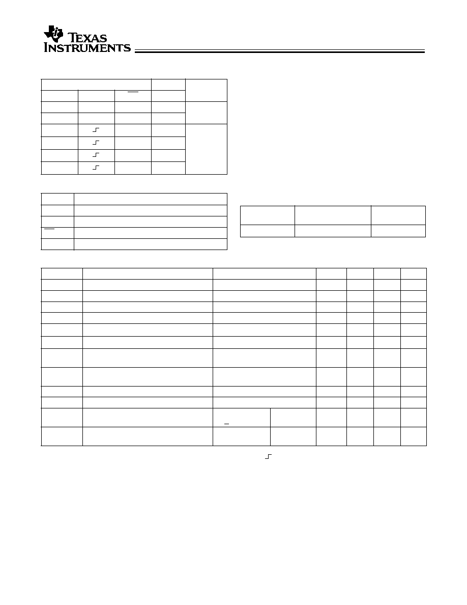
Function Table
[1]
Inputs
Outputs
Function
D
CLK
OE
O
X
L
H
Z
High-Z
X
H
H
Z
L
L
L
Load
Register
H
L
H
L
H
Z
H
H
Z
Pin Description
Name
Description
D
Data Inputs
[2]
CLK
Clock Inputs
OE
Three-State Output Enable Inputs (Active LOW)
O
Three-State Outputs
Operating Range
Range
Ambient
Temperature
V
CC
Industrial
-
40
∞
C to +85
∞
C
2.7V to 3.6V
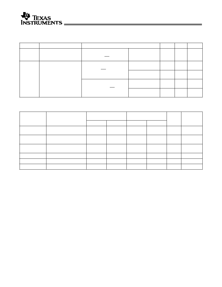
Electrical Characteristics for Non Bus Hold Devices
Over the Operating Range V
CC
=2.7V to 3.6V
Parameter
Description
Test Conditions
Min.
Typ.
[5]
Max.
Unit
V
IH
Input HIGH Voltage
All Inputs
2.0
5.5
V
V
IL
Input LOW Voltage
0.8
V
V
H
Input Hysteresis
[6]
100
mV
V
IK
Input Clamp Diode Voltage
V
CC
=Min., I
IN
=≠18 mA
≠0.7
≠1.2
V
I
IH
Input HIGH Current
V
CC
=Max., V
I
=5.5
±
1
µ
A
I
IL
Input LOW Current
V
CC
=Max., V
I
=GND
±
1
µ
A
I
OZH
High Impedance Output Current
(Three-State Output pins)
V
CC
=Max., V
OUT
=5.5V
±
1
µ
A
I
OZL
High Impedance Output Current
(Three-State Output pins)
V
CC
=Max., V
OUT
=GND
±
1
µ
A
I
OS
Short Circuit Current
[7]
V
CC
=Max., V
OUT
=GND
≠60
≠135
≠240
mA
I
OFF
Power-Off Disable
V
CC
=0V, V
OUT
4.5V
±
100
µ
A
I
CC
Quiescent Power Supply Current
V
IN
0.2V,
V
IN
>V
CC
≠0.2V
V
CC
=Max.
0.1
10
µ
A
I
CC
Quiescent Power Supply Current
(TTL inputs HIGH)
V
IN
=V
CC
≠0.6V
[8]
V
CC
=Max.
2.0
30
µ
A
Notes:
1.
H = HIGH Voltage Level. L = LOW Voltage Level. X = Don't Care. Z = HIGH Impedance.
= LOW-to-HIGH Transition.
2.
On the CY74FCT163H374, these pins have "bus hold."
3.
Operation beyond the limits set forth may impair the useful life of the device. Unless otherwise noted, these limits are over the operating free-air temperature
range.
4.
Unused inputs must always be connected to an appropriate logic voltage level, preferably either V
CC
or ground
5.
Typical values are at V
CC
=3.3V, T
A
= +25∞C ambient.
6.
This parameter is specified but not tested.
7.
Not more than one output should be shorted at a time. Duration of short should not exceed one second. The use of high-speed test apparatus and/or sample
and hold techniques are preferable in order to minimize internal chip heating and more accurately reflect operational values. Otherwise prolonged shorting of
a high output may raise the chip temperature well above normal and thereby cause invalid readings in other parametric tests. In any sequence of parameter
tests, I
OS
tests should be performed last.
8.
Per TTL driven input; all other inputs at V
CC
or GND.

CY74FCT163374
CY74FCT163H374
3
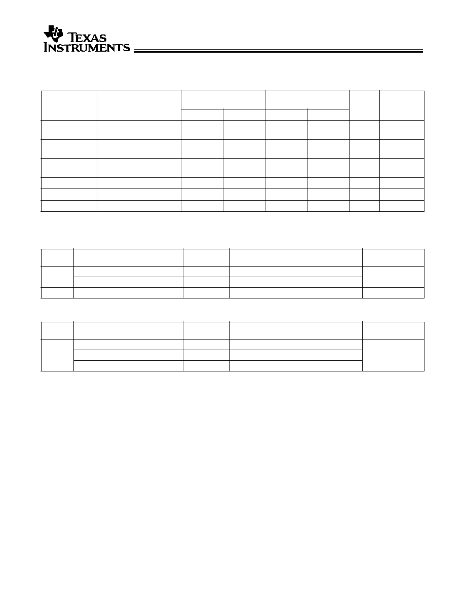
Electrical Characteristics For Bus Hold Devices
Over the Operating Range V
CC
=2.7V to 3.6V
Parameter
Description
Test Conditions
Min.
Typ.
[5]
Max.
Unit
V
IH
Input HIGH Voltage
All Inputs
2.0
V
CC
V
V
IL
Input LOW Voltage
0.8
V
V
H
Input Hysteresis
[6]
100
mV
V
IK
Input Clamp Diode Voltage
V
CC
=Min., I
IN
=≠18 mA
≠0.7
≠ 1.2
V
I
IH
Input HIGH Current
V
CC
=Max., V
I
=V
CC
±
100
µ
A
I
IL
Input LOW Current
±
100
µ
A
I
BBH
I
BBL
Bus Hold Sustain Current on Bus Hold Input
[9]
V
CC
=Min.
V
I
=2.0V
≠50
µ
A
V
I
=0.8V
+50
µ
A
I
BHHO
I
BHLO
Bus Hold Overdrive Current on Bus Hold In-
put
[9]
V
CC
=Max., V
I
=1.5V
±
500
µ
A
I
OZH
High Impedance Output Current
(Three-State Output pins)
V
CC
=Max., V
OUT
=V
CC
±
1
µ
A
I
OZL
High Impedance Output Current
(Three-State Output pins)
V
CC
=Max., V
OUT
=GND
±
1
µ
A
I
OS
Short Circuit Current
[7]
V
CC
=Max., V
OUT
=GND
≠60
≠135
≠240
mA
I
OFF
Power-Off Disable
V
CC
=0V, V
OUT
4.5V
±
100
µ
A
I
CC
Quiescent Power Supply Current
V
IN
<0.2V
V
CC
=Max.
+40
µ
A
ICC
Quiescent Power supply Current
(TTL inputs HIGH)
V
IN
=V
CC
≠0.6V
[8]
V
CC
=Max.
+350
µ
A
Electrical Characteristics For Balanced Drive Devices
Over the Operating Range V
CC
=2.7V to 3.6V
Parameter
Description
Test Conditions
Min.
Typ.
[5]
Max.
Unit
I
ODL
Output LOW Dynamic Current
[7]
V
CC
=3.3V, V
IN
=V
IH
or V
IL
, V
OUT
=1.5V
45
110
mA
I
ODH
Output HIGH Dynamic Current
[7]
V
CC
=3.3V, V
IN
=V
IH
or V
IL
, V
OUT
=1.5V
≠45
≠110
mA
V
OH
Output HIGH Voltage
V
CC
=Min., I
OH
= ≠0.1 mA
V
CC
≠0.2
V
V
CC
=Min., I
OH
= ≠8 mA
2.4
[10]
3.0
V
V
CC
=3.0V, I
OH
= ≠24 mA
2.0
3.0
V
V
OL
Output LOW Voltage
V
CC
=Min., I
OL
= 0.1mA
0.2
V
V
CC
=Min., I
OL
= 24 mA
0.3
0.55
Notes:
9.
Pins with bus hold are described in Pin Description.
10. V
OH
=V
CC
≠0.6V at rated current.
Capacitance
[6]
(T
A
= +25∞C, f = 1.0 MHz)
Parameter
Description
Test Conditions
Typ.
[5]
Max.
Unit
C
IN
Input Capacitance
V
IN
= 0V
4.5
6.0
pF
C
OUT
Output Capacitance
V
OUT
= 0V
5.5
8.0
pF
CY74FCT163374
CY74FCT163H374
4
Power Supply Characteristics
Parameter
Description
Test Conditions
Typ.
[5]
Max.
Unit
I
CCD
Dynamic Power Supply
Current
[11]
V
CC
=Max., One Input Toggling,
50% Duty Cycle,
Outputs Open, OE=GND
V
IN
=V
CC
or
V
IN
=GND
50
75
µ
A/MHz
I
C
Total Power Supply
Current
[12]
V
CC
=Max., f
1
=10 MHz, 50%
Duty Cycle, Outputs Open, One
Bit Toggling, OE=GND
V
IN
=V
CC
or
V
IN
=GND
0.5
0.8
mA
V
IN
=V
CC
≠0.6V or
V
IN
=GND
0.5
0.8
mA
V
CC
=Max., f
1
=2.5 MHz, 50%
Duty Cycle, Outputs Open, Six-
teen Bits Toggling, OE=GND
V
IN
=V
CC
or
V
IN
=GND
2.0
3.0
[13]
mA
V
IN
=V
CC
≠0.6V or
V
IN
=GND
2.0
3.3
[13]
mA
Switching Characteristics
Over the Operating Range V
CC
=3.0V to 3.6V
[14,15]
Parameter
Description
CY74FCT163374A
CY74FCT163H374A
CY74FCT163374C
CY74FCT163H374C
Min.
Max.
Min.
Max.
Unit
Fig. No.
[16]
t
PLH
t
PHL
Propagation Delay Clock to
Output
1.5
6.5
1.5
5.2
ns
1, 3
t
PZH
t
PZL
Output Enable Time
1.5
6.5
1.5
5.5
ns
1, 7, 8
t
PHZ
t
PLZ
Output Disable Time
1.5
5.5
1.5
5.0
ns
1, 7, 8
t
SU
Input Setup time
2.0
2.0
ns
1, 4
t
H
Input Hold time
1.5
-
1.5
-
ns
1. 4
t
SK(O)
Output Skew
[17]
0.5
0.5
ns
--
Notes:
11. This parameter is not directly testable, but is derived for use in Total Power Supply calculations.
12. I
C
= I
QUIESCENT
+ I
INPUTS
+ I
DYNAMIC
I
C
= I
CC
+
I
CC
D
H
N
T
+I
CCD
(f
0
/2 + f
1
N
1
)
I
CC
= Quiescent Current with CMOS input levels
I
CC
= Power Supply Current for a TTL HIGH input (V
IN
=3.4V)
D
H
= Duty Cycle for TTL inputs HIGH
N
T
= Number of TTL inputs at D
H
I
CCD
= Dynamic Current caused by an input transition pair (HLH or LHL)
f
0
= Clock frequency for registered devices, otherwise zero
f
1
= Input signal frequency
N
1
= Number of inputs changing at f
1
All currents are in milliamps and all frequencies are in megahertz.
13. Values for these conditions are examples of the I
CC
formula. These limits are specified but not tested.
14. Minimum limits are specified but not tested on Propagation Delays.
15. For V
CC
=2.7, propagation delay, output enable and output disable times should be degraded by 20%.
16. See "Parameter Measurement Information" in the General Information section.
17. Skew between any two outputs of the same package switching in the same direction. This parameter is ensured by design.
CY74FCT163374
CY74FCT163H374
5
Switching Characteristics
Over the Operating Range V
CC
=3.0V to 3.6V
[14,15]
Parameter
Description
CY74FCT163LD374
[18]
CY74FCT163LDH374
CY74FCT163LD374A
[18]
CY74FCT163LDH374A
Min.
Max.
Min.
Max.
Unit
Fig. No.
[16]
t
PLH
t
PHL
Propagation Delay Clock to
Q Output
1.5
10
1.5
6.5
ns
1, 3
t
PZH
t
PZL
Output Enable Time
1.5
12.5
1.5
6.5
ns
1, 7, 8
t
PHZ
t
PLZ
Output Disable Time
1.5
8.0
1.5
5.5
ns
1, 7, 8
t
SU
Input Setup time
2.0
2.0
ns
1, 4
t
H
Input Hold time
1.5
1.5
ns
1, 4
t
SK(O)
Output Skew
[17]
0.5
0.5
ns
--
Note:
18. For Lite Drive devices the load capacitance is 30 pF. For all others it is 50 pF.
Ordering Information CY74FCT163374
Speed
(ns)
Ordering Code
Package
Name
Package Type
Operating
Range
5.2
CY74FCT163374CPACT
Z48
48-Lead (240-Mil) TSSOP
Industrial
CY74FCT163374CPVC/PVCT
O48
48-Lead (300-Mil) SSOP
6.5
CY74FCT163374APACT
Z48
48-Lead (240-Mil) TSSOP
Industrial
Ordering Information CY74FCT163H374
Speed
(ns)
Ordering Code
Package
Name
Package Type
Operating
Range
5.2
74FCT163H374CPACT
Z48
48-Lead (240-Mil) TSSOP
Industrial
CY74FCT163H374CPVC
O48
48-Lead (300-Mil) SSOP
74FCT163H374CPVCT
O48
48-Lead (300-Mil) SSOP
CY74FCT163374
CY74FCT163H374
6
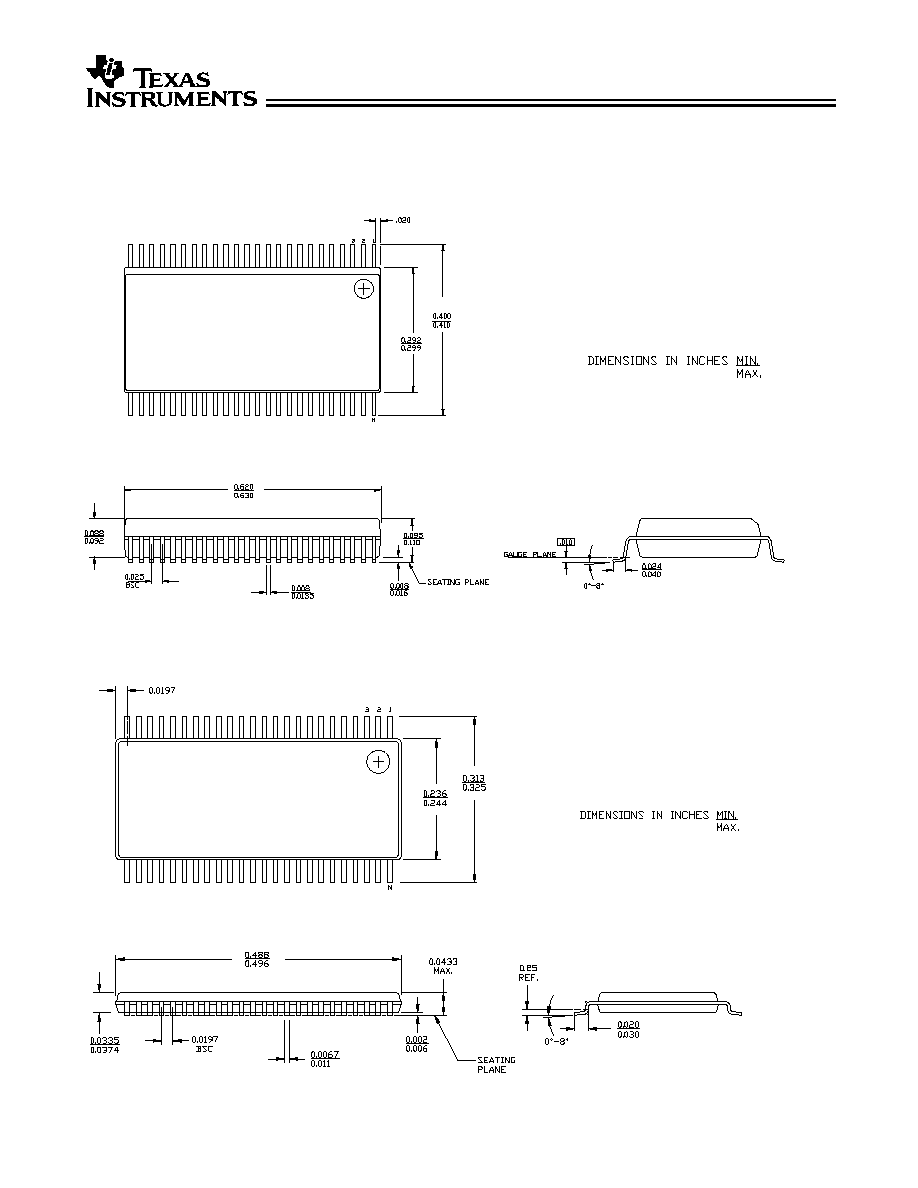
D
Package Diagrams
48-Lead Shrunk Small Outline Package O48
48-Lead Thin Shrunk Small Outline Package Z48

PACKAGING INFORMATION
Orderable Device
Status
(1)
Package
Type
Package
Drawing
Pins Package
Qty
Eco Plan
(2)
Lead/Ball Finish
MSL Peak Temp
(3)
74FCT163H374CPACT
OBSOLETE
TSSOP
DGG
48
TBD
Call TI
Call TI
74FCT163H374CPVCT
OBSOLETE
SSOP
DL
48
TBD
Call TI
Call TI
CY74FCT163374APAC
OBSOLETE
TSSOP
DGG
48
TBD
Call TI
Call TI
CY74FCT163374APACT
OBSOLETE
TSSOP
DGG
48
TBD
Call TI
Call TI
CY74FCT163374CPAC
OBSOLETE
TSSOP
DGG
48
TBD
Call TI
Call TI
CY74FCT163374CPACT
OBSOLETE
TSSOP
DGG
48
TBD
Call TI
Call TI
CY74FCT163374CPVC
OBSOLETE
SSOP
DL
48
TBD
Call TI
Call TI
CY74FCT163374CPVCT
OBSOLETE
SSOP
DL
48
TBD
Call TI
Call TI
CY74FCT163H374CPAC
OBSOLETE
TSSOP
DGG
48
TBD
Call TI
Call TI
CY74FCT163H374CPVC
OBSOLETE
SSOP
DL
48
TBD
Call TI
Call TI
(1)
The marketing status values are defined as follows:
ACTIVE: Product device recommended for new designs.
LIFEBUY: TI has announced that the device will be discontinued, and a lifetime-buy period is in effect.
NRND: Not recommended for new designs. Device is in production to support existing customers, but TI does not recommend using this part in
a new design.
PREVIEW: Device has been announced but is not in production. Samples may or may not be available.
OBSOLETE: TI has discontinued the production of the device.
(2)
Eco
Plan
-
The
planned
eco-friendly
classification:
Pb-Free
(RoHS)
or
Green
(RoHS
&
no
Sb/Br)
-
please
check
http://www.ti.com/productcontent
for the latest availability information and additional product content details.
TBD: The Pb-Free/Green conversion plan has not been defined.
Pb-Free (RoHS): TI's terms "Lead-Free" or "Pb-Free" mean semiconductor products that are compatible with the current RoHS requirements
for all 6 substances, including the requirement that lead not exceed 0.1% by weight in homogeneous materials. Where designed to be soldered
at high temperatures, TI Pb-Free products are suitable for use in specified lead-free processes.
Green (RoHS & no Sb/Br): TI defines "Green" to mean Pb-Free (RoHS compatible), and free of Bromine (Br) and Antimony (Sb) based flame
retardants (Br or Sb do not exceed 0.1% by weight in homogeneous material)
(3)
MSL, Peak Temp. -- The Moisture Sensitivity Level rating according to the JEDEC industry standard classifications, and peak solder
temperature.
Important Information and Disclaimer:The information provided on this page represents TI's knowledge and belief as of the date that it is
provided. TI bases its knowledge and belief on information provided by third parties, and makes no representation or warranty as to the
accuracy of such information. Efforts are underway to better integrate information from third parties. TI has taken and continues to take
reasonable steps to provide representative and accurate information but may not have conducted destructive testing or chemical analysis on
incoming materials and chemicals. TI and TI suppliers consider certain information to be proprietary, and thus CAS numbers and other limited
information may not be available for release.
In no event shall TI's liability arising out of such information exceed the total purchase price of the TI part(s) at issue in this document sold by TI
to Customer on an annual basis.
PACKAGE OPTION ADDENDUM
www.ti.com
30-Mar-2005
Addendum-Page 1
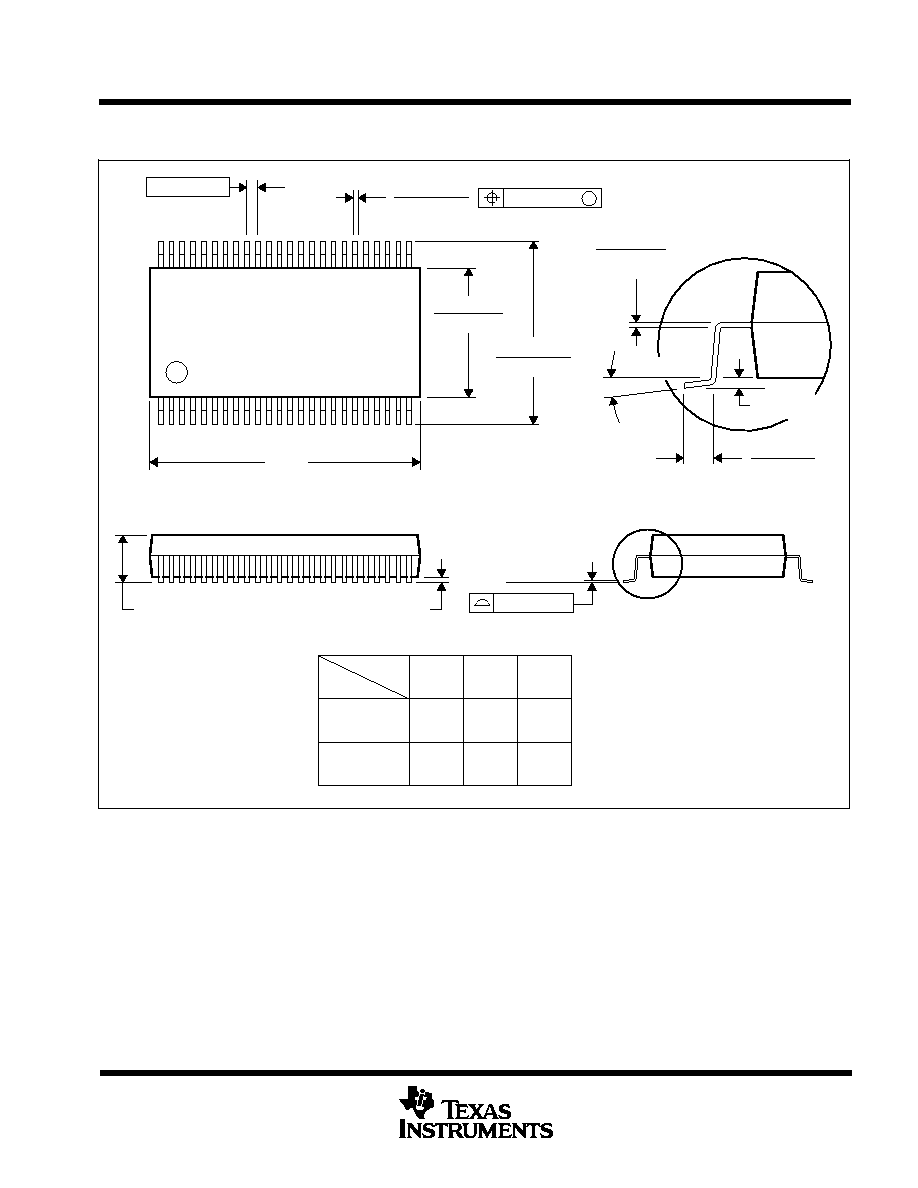
MECHANICAL DATA
MSSO001C ≠ JANUARY 1995 ≠ REVISED DECEMBER 2001
POST OFFICE BOX 655303
∑
DALLAS, TEXAS 75265
DL (R-PDSO-G**)
PLASTIC SMALL-OUTLINE PACKAGE
4040048 / E 12/01
48 PINS SHOWN
56
0.730
(18,54)
0.720
(18,29)
48
28
0.370
(9,40)
(9,65)
0.380
Gage Plane
DIM
0.420 (10,67)
0.395 (10,03)
A MIN
A MAX
0.010 (0,25)
PINS **
0.630
(16,00)
(15,75)
0.620
0.010 (0,25)
Seating Plane
0.020 (0,51)
0.040 (1,02)
25
24
0.008 (0,203)
0.0135 (0,343)
48
1
0.008 (0,20) MIN
A
0.110 (2,79) MAX
0.299 (7,59)
0.291 (7,39)
0.004 (0,10)
M
0.005 (0,13)
0.025 (0,635)
0
∞
≠ 8
∞
0.005 (0,13)
NOTES: A. All linear dimensions are in inches (millimeters).
B. This drawing is subject to change without notice.
C. Body dimensions do not include mold flash or protrusion not to exceed 0.006 (0,15).
D. Falls within JEDEC MO-118
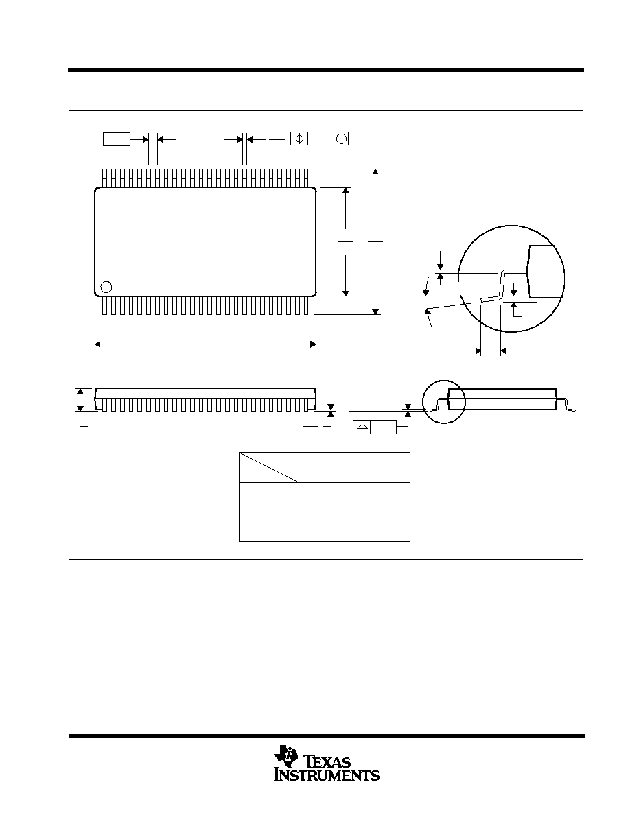
MECHANICAL DATA
MTSS003D ≠ JANUARY 1995 ≠ REVISED JANUARY 1998
POST OFFICE BOX 655303
∑
DALLAS, TEXAS 75265
DGG (R-PDSO-G**)
PLASTIC SMALL-OUTLINE PACKAGE
4040078 / F 12/97
48 PINS SHOWN
0,25
0,15 NOM
Gage Plane
6,00
6,20
8,30
7,90
0,75
0,50
Seating Plane
25
0,27
0,17
24
A
48
1
1,20 MAX
M
0,08
0,10
0,50
0
∞
≠ 8
∞
56
14,10
13,90
48
DIM
A MAX
A MIN
PINS **
12,40
12,60
64
17,10
16,90
0,15
0,05
NOTES: A. All linear dimensions are in millimeters.
B. This drawing is subject to change without notice.
C. Body dimensions do not include mold protrusion not to exceed 0,15.
D. Falls within JEDEC MO-153

IMPORTANT NOTICE
Texas Instruments Incorporated and its subsidiaries (TI) reserve the right to make corrections, modifications,
enhancements, improvements, and other changes to its products and services at any time and to discontinue
any product or service without notice. Customers should obtain the latest relevant information before placing
orders and should verify that such information is current and complete. All products are sold subject to TI's terms
and conditions of sale supplied at the time of order acknowledgment.
TI warrants performance of its hardware products to the specifications applicable at the time of sale in
accordance with TI's standard warranty. Testing and other quality control techniques are used to the extent TI
deems necessary to support this warranty. Except where mandated by government requirements, testing of all
parameters of each product is not necessarily performed.
TI assumes no liability for applications assistance or customer product design. Customers are responsible for
their products and applications using TI components. To minimize the risks associated with customer products
and applications, customers should provide adequate design and operating safeguards.
TI does not warrant or represent that any license, either express or implied, is granted under any TI patent right,
copyright, mask work right, or other TI intellectual property right relating to any combination, machine, or process
in which TI products or services are used. Information published by TI regarding third-party products or services
does not constitute a license from TI to use such products or services or a warranty or endorsement thereof.
Use of such information may require a license from a third party under the patents or other intellectual property
of the third party, or a license from TI under the patents or other intellectual property of TI.
Reproduction of information in TI data books or data sheets is permissible only if reproduction is without
alteration and is accompanied by all associated warranties, conditions, limitations, and notices. Reproduction
of this information with alteration is an unfair and deceptive business practice. TI is not responsible or liable for
such altered documentation.
Resale of TI products or services with statements different from or beyond the parameters stated by TI for that
product or service voids all express and any implied warranties for the associated TI product or service and
is an unfair and deceptive business practice. TI is not responsible or liable for any such statements.
Following are URLs where you can obtain information on other Texas Instruments products and application
solutions:
Products
Applications
Amplifiers
amplifier.ti.com
Audio
www.ti.com/audio
Data Converters
dataconverter.ti.com
Automotive
www.ti.com/automotive
DSP
dsp.ti.com
Broadband
www.ti.com/broadband
Interface
interface.ti.com
Digital Control
www.ti.com/digitalcontrol
Logic
logic.ti.com
Military
www.ti.com/military
Power Mgmt
power.ti.com
Optical Networking
www.ti.com/opticalnetwork
Microcontrollers
microcontroller.ti.com
Security
www.ti.com/security
Telephony
www.ti.com/telephony
Video & Imaging
www.ti.com/video
Wireless
www.ti.com/wireless
Mailing Address:
Texas Instruments
Post Office Box 655303 Dallas, Texas 75265
Copyright
2005, Texas Instruments Incorporated