 | –≠–ª–µ–∫—Ç—Ä–æ–Ω–Ω—ã–π –∫–æ–º–ø–æ–Ω–µ–Ω—Ç: 74LVC244 | –°–∫–∞—á–∞—Ç—å:  PDF PDF  ZIP ZIP |
SN74LVC244A
OCTAL BUFFER/DRIVER
WITH 3-STATE OUTPUTS
SCAS414L ≠ NOVEMBER 1992 ≠ REVISED APRIL 1999
1
POST OFFICE BOX 655303
∑
DALLAS, TEXAS 75265
D
EPIC
TM
(Enhanced-Performance Implanted
CMOS) Submicron Process
D
Typical V
OLP
(Output Ground Bounce)
<0.8 V at V
CC
= 3.3 V, T
A
= 25
∞
C
D
Typical V
OHV
(Output V
OH
Undershoot) >2 V
at V
CC
= 3.3 V, T
A
= 25
∞
C
D
Power Off Disables Outputs, Permitting
Live Insertion
D
Supports Mixed-Mode Signal Operation on
All Ports (5-V Input/Output Voltage With
3.3-V V
CC
)
D
ESD Protection Exceeds 2000 V Per
MIL-STD-883, Method 3015; Exceeds 200 V
Using Machine Model (C = 200 pF, R = 0)
D
Latch-Up Performance Exceeds 250 mA Per
JESD 17
D
Package Options Include Shrink
Small-Outline (DB), Plastic Small-Outline
(DW), and Thin Shrink Small-Outline (PW)
Packages
description
This octal buffer/line driver is operational at 1.5-V to 3.6-V V
CC
, but designed specifically for 1.65-V to 3.6-V V
CC
operation.
The SN74LVC244A is organized as two 4-bit line drivers with separate output-enable (OE) inputs. When OE
is low, the device passes data from the A inputs to the Y outputs. When OE is high, the outputs are in the
high-impedance state.
Inputs can be driven from either 3.3-V or 5-V devices. This feature allows the use of these devices as translators
in a mixed 3.3-V/5-V system environment.
To ensure the high-impedance state during power up or power down, OE should be tied to V
CC
through a pullup
resistor; the minimum value of the resistor is determined by the current-sinking capability of the driver.
The SN74LVC244A is characterized for operation from ≠40
∞
C to 85
∞
C.
FUNCTION TABLE
(each buffer)
INPUTS
OUTPUT
OE
A
Y
L
H
H
L
L
L
H
X
Z
Copyright
©
1999, Texas Instruments Incorporated
PRODUCTION DATA information is current as of publication date.
Products conform to specifications per the terms of Texas Instruments
standard warranty. Production processing does not necessarily include
testing of all parameters.
Please be aware that an important notice concerning availability, standard warranty, and use in critical applications of
Texas Instruments semiconductor products and disclaimers thereto appears at the end of this data sheet.
EPIC is a trademark of Texas Instruments Incorporated.
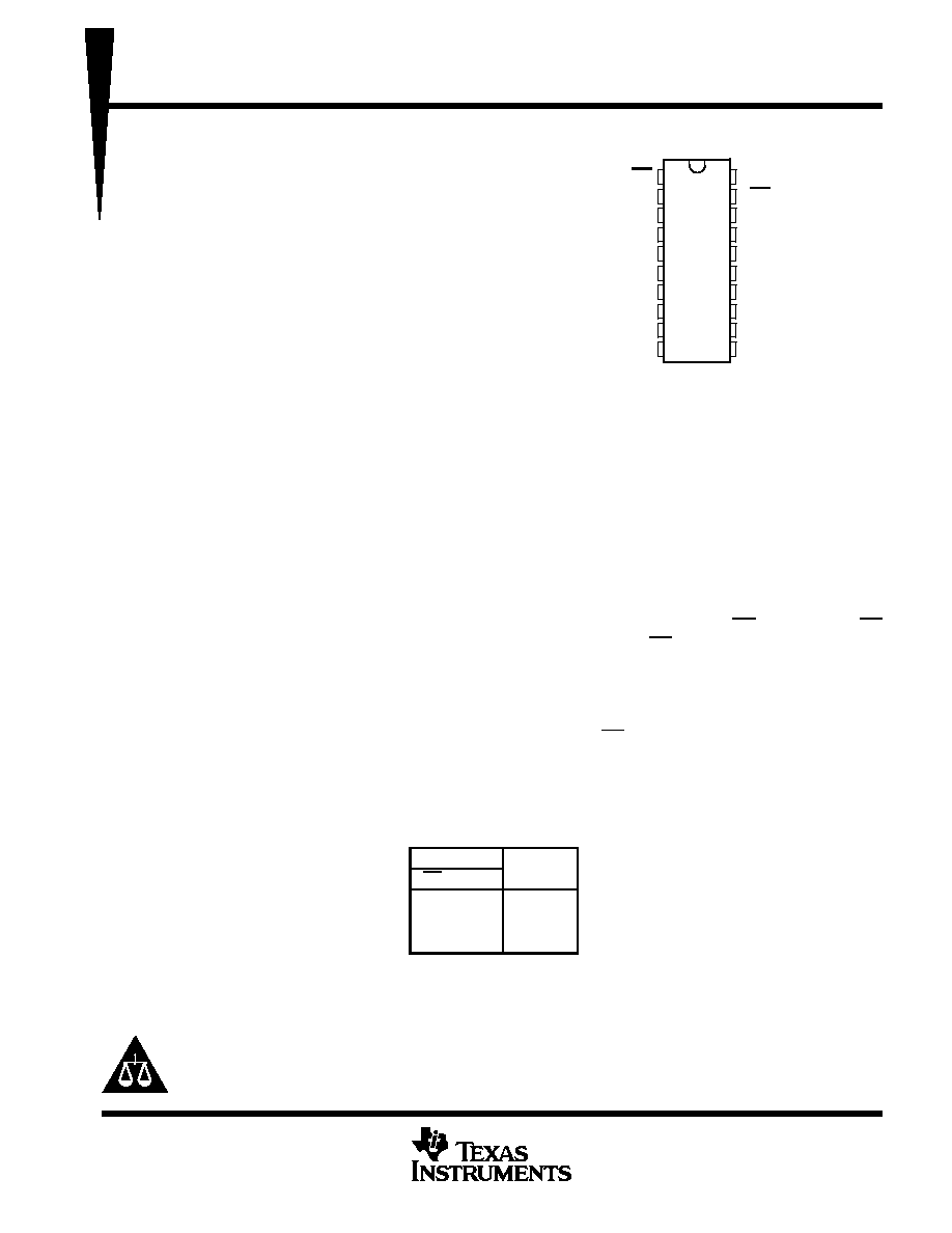
1
2
3
4
5
6
7
8
9
10
20
19
18
17
16
15
14
13
12
11
1OE
1A1
2Y4
1A2
2Y3
1A3
2Y2
1A4
2Y1
GND
V
CC
2OE
1Y1
2A4
1Y2
2A3
1Y3
2A2
1Y4
2A1
DB, DW, OR PW PACKAGE
(TOP VIEW)
SN74LVC244A
OCTAL BUFFER/DRIVER
WITH 3-STATE OUTPUTS
SCAS414L ≠ NOVEMBER 1992 ≠ REVISED APRIL 1999
2
POST OFFICE BOX 655303
∑
DALLAS, TEXAS 75265
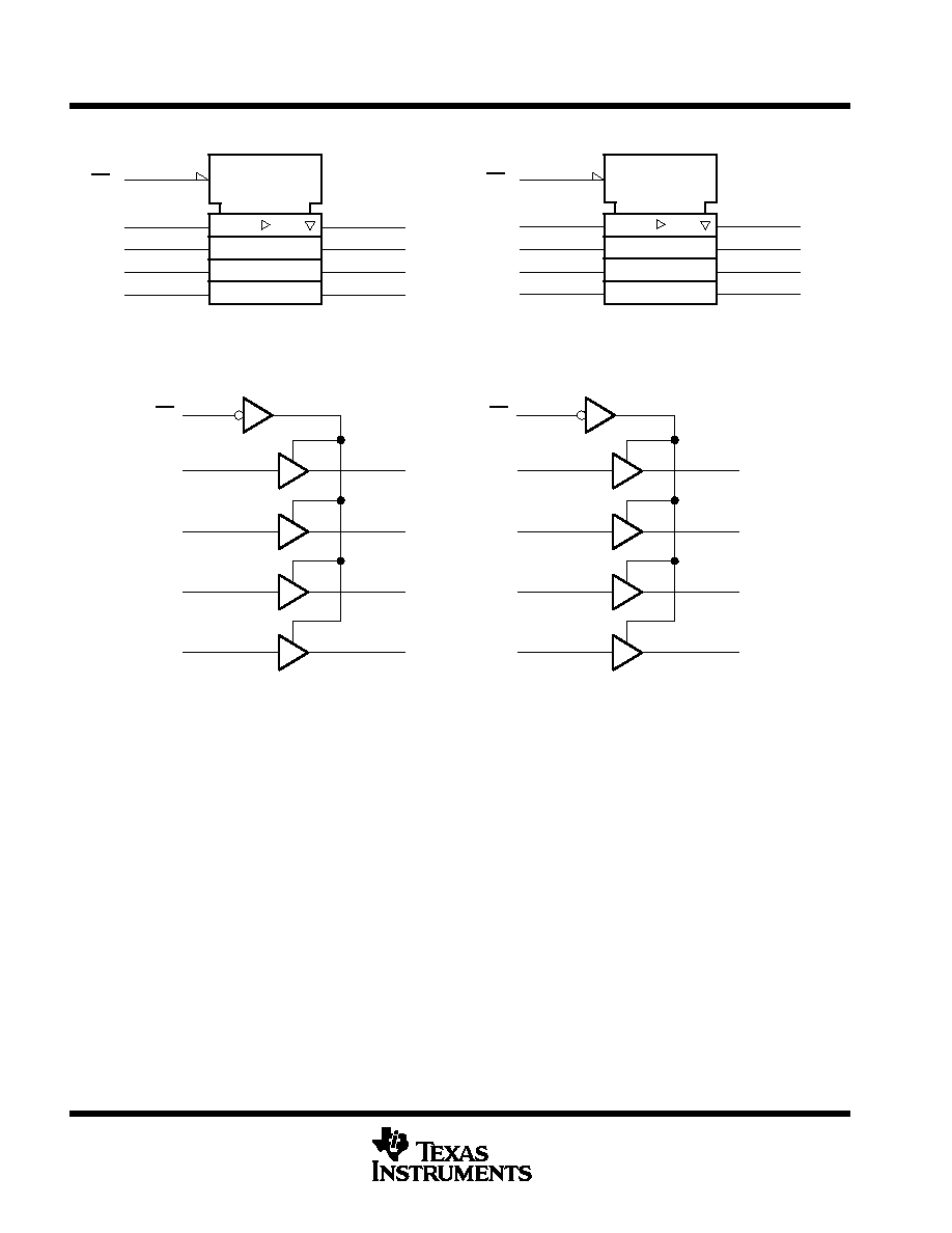
logic symbol
2
1A1
4
1A2
6
1A3
8
1A4
EN
1
1Y1
18
1Y2
16
1Y3
14
1Y4
12
11
2A1
13
2A2
15
2A3
17
2A4
EN
19
2Y1
9
2Y2
7
2Y3
5
2Y4
3
1OE
2OE
This symbol is in accordance with ANSI/IEEE Std 91-1984 and IEC Publication 617-12.
logic diagram (positive logic)
1
2
18
1Y1
1OE
1A1
4
16
1Y2
1A2
6
14
1Y3
1A3
8
12
1Y4
1A4
19
11
9
2Y1
2OE
2A1
13
7
2Y2
2A2
15
5
2Y3
2A3
17
3
2Y4
2A4
absolute maximum ratings over operating free-air temperature range (unless otherwise noted)
Supply voltage range, V
CC
≠0.5 V to 6.5 V
. . . . . . . . . . . . . . . . . . . . . . . . . . . . . . . . . . . . . . . . . . . . . . . . . . . . . . . . .
Input voltage range, V
I
(see Note 1)
≠0.5 V to 6.5 V
. . . . . . . . . . . . . . . . . . . . . . . . . . . . . . . . . . . . . . . . . . . . . . . . .
Voltage range applied to any output in the high-impedance or power-off state, V
O
(see Note 1)
≠0.5 V to 6.5 V
. . . . . . . . . . . . . . . . . . . . . . . . . . . . . . . . . . . . . . . . . . . . . . . . . . . . . . . . . . . . . . . . . . .
Voltage range applied to any output in the high or low state, V
O
(see Notes 1 and 2)
≠0.5 V to V
CC
+ 0.5 V
. . . . . . . . . . . . . . . . . . . . . . . . . . . . . . . . . . . . . . . . . . . . . . . . . . . . . . .
Input clamp current, I
IK
(V
I
< 0 )
≠50 mA
. . . . . . . . . . . . . . . . . . . . . . . . . . . . . . . . . . . . . . . . . . . . . . . . . . . . . . . . . .
Output clamp current, I
OK
(V
O
< 0)
≠50 mA
. . . . . . . . . . . . . . . . . . . . . . . . . . . . . . . . . . . . . . . . . . . . . . . . . . . . . . . .
Continuous output current, I
O
±
50 mA
. . . . . . . . . . . . . . . . . . . . . . . . . . . . . . . . . . . . . . . . . . . . . . . . . . . . . . . . . . . . .
Continuous current through V
CC
or GND
±
100 mA
. . . . . . . . . . . . . . . . . . . . . . . . . . . . . . . . . . . . . . . . . . . . . . . . . .
Package thermal impedance,
JA
(see Note 3): DB package
115
∞
C/W
. . . . . . . . . . . . . . . . . . . . . . . . . . . . . . . .
DW package
97
∞
C/W
. . . . . . . . . . . . . . . . . . . . . . . . . . . . . . . . .
PW package
128
∞
C/W
. . . . . . . . . . . . . . . . . . . . . . . . . . . . . . . .
Storage temperature range, T
stg
≠65
∞
C to 150
∞
C
. . . . . . . . . . . . . . . . . . . . . . . . . . . . . . . . . . . . . . . . . . . . . . . . . . .
Stresses beyond those listed under "absolute maximum ratings" may cause permanent damage to the device. These are stress ratings only, and
functional operation of the device at these or any other conditions beyond those indicated under "recommended operating conditions" is not
implied. Exposure to absolute-maximum-rated conditions for extended periods may affect device reliability.
NOTES:
1. The input negative-voltage and output voltage ratings may be exceeded if the input and output current ratings are observed.
2. The value of VCC is provided in the recommended operating conditions table.
3. The package thermal impedance is calculated in accordance with JESD 51.
SN74LVC244A
OCTAL BUFFER/DRIVER
WITH 3-STATE OUTPUTS
SCAS414L ≠ NOVEMBER 1992 ≠ REVISED APRIL 1999
3
POST OFFICE BOX 655303
∑
DALLAS, TEXAS 75265
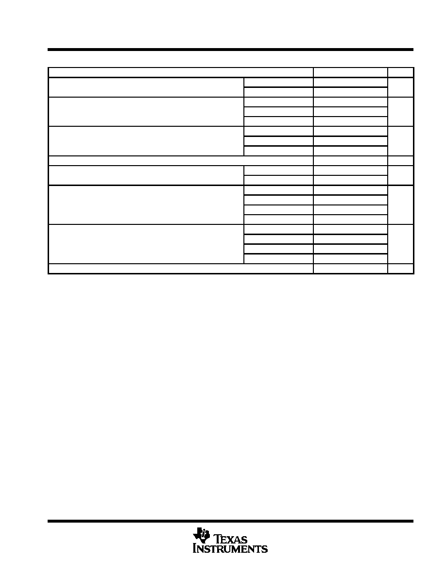
recommended operating conditions (see Note 4)
MIN
MAX
UNIT
VCC
Supply voltage
Operating
1.65
3.6
V
VCC
Supply voltage
Data retention only
1.5
V
VCC = 1.65 V to 1.95 V
0.65
◊
VCC
VIH
High-level input voltage
VCC = 2.3 V to 2.7 V
1.7
V
VCC = 2.7 V to 3.6 V
2
VCC = 1.65 V to 1.95 V
0.35
◊
VCC
VIL
Low-level input voltage
VCC = 2.3 V to 2.7 V
0.7
V
VCC = 2.7 V to 3.6 V
0.8
VI
Input voltage
0
5.5
V
VO
Output voltage
High or low state
0
VCC
V
VO
Output voltage
3 state
0
5.5
V
VCC = 1.65 V
≠4
IOH
High level output current
VCC = 2.3 V
≠8
mA
IOH
High-level output current
VCC = 2.7 V
≠12
mA
VCC = 3 V
≠24
VCC = 1.65 V
4
IOL
Low level output current
VCC = 2.3 V
8
mA
IOL
Low-level output current
VCC = 2.7 V
12
mA
VCC = 3 V
24
TA
Operating free-air temperature
≠40
85
∞
C
NOTE 4: All unused inputs of the device must be held at VCC or GND to ensure proper device operation. Refer to the TI application report,
Implications of Slow or Floating CMOS Inputs, literature number SCBA004.
SN74LVC244A
OCTAL BUFFER/DRIVER
WITH 3-STATE OUTPUTS
SCAS414L ≠ NOVEMBER 1992 ≠ REVISED APRIL 1999
4
POST OFFICE BOX 655303
∑
DALLAS, TEXAS 75265
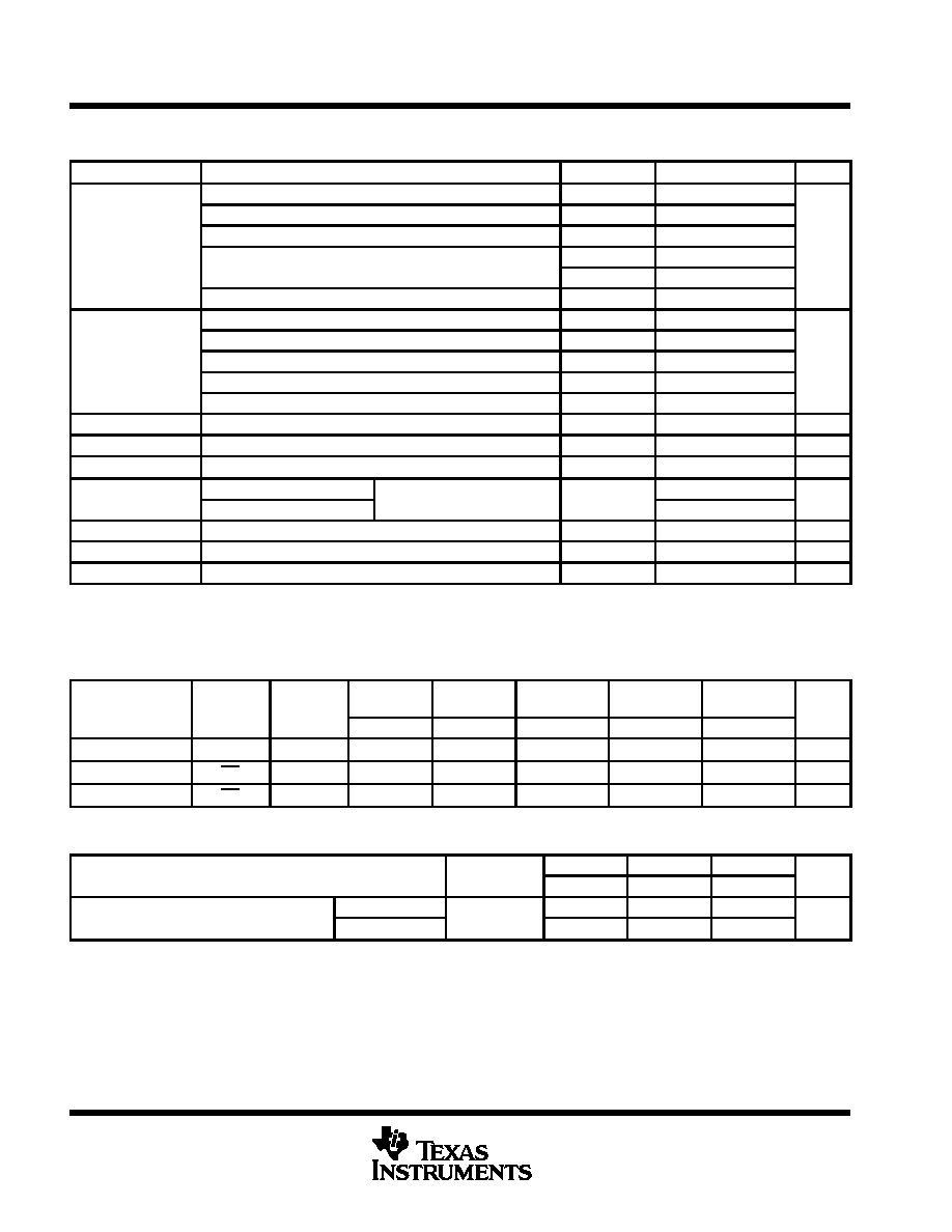
electrical characteristics over recommended operating free-air temperature range (unless
otherwise noted)
PARAMETER
TEST CONDITIONS
VCC
MIN
TYP
MAX
UNIT
IOH = ≠100
µ
A
1.65 V to 3.6 V
VCC≠0.2
IOH = ≠4 mA
1.65 V
1.2
VOH
IOH = ≠8 mA
2.3 V
1.7
V
VOH
IOH = 12 mA
2.7 V
2.2
V
IOH = ≠12 mA
3 V
2.4
IOH = ≠24 mA
3 V
2.2
IOL = 100
µ
A
1.65 V to 3.6 V
0.2
IOL = 4 mA
1.65 V
0.45
VOL
IOL = 8 mA
2.3 V
0.7
V
IOL = 12 mA
2.7 V
0.4
IOL = 24 mA
3 V
0.55
II
VI = 0 to 5.5 V
3.6 V
±
5
µ
A
Ioff
VI or VO = 5.5 V
0
±
10
µ
A
IOZ
VO = 0 to 5.5 V
3.6 V
±
10
µ
A
ICC
VI = VCC or GND
IO = 0
3 6 V
10
µ
A
ICC
3.6 V
VI
5.5 V
IO = 0
3.6 V
10
µ
A
ICC
One input at VCC ≠ 0.6 V,
Other inputs at VCC or GND
2.7 V to 3.6 V
500
µ
A
Ci
VI = VCC or GND
3.3 V
4
pF
Co
VO = VCC or GND
3.3 V
5.5
pF
All typical values are at VCC = 3.3 V, TA = 25
∞
C.
This applies in the disabled state only.
switching characteristics over recommended operating free-air temperature range (unless
otherwise noted) (see Figures 1 through 4)
PARAMETER
FROM
(INPUT)
TO
(OUTPUT)
VCC = 1.5 V VCC = 1.8 V
VCC = 2.5 V
±
0.2 V
VCC = 2.7 V
VCC = 3.3 V
±
0.3 V
UNIT
(INPUT)
(OUTPUT)
TYP
TYP
MIN
MAX
MIN
MAX
MIN
MAX
tpd
A
Y
5.75
12
1
7.9
6.9
1.5
5.9
ns
ten
OE
Y
6.59
13.1
1
9.6
8.6
1.5
7.6
ns
tdis
OE
Y
5.7
14.6
1
7.8
6.8
1.5
6.5
ns
operating characteristics, T
A
= 25
∞
C
PARAMETER
TEST
VCC = 1.8 V VCC = 2.5 V VCC = 3.3 V
UNIT
PARAMETER
CONDITIONS
TYP
TYP
TYP
UNIT
Cpd
Power dissipation capacitance
Outputs enabled
f = 10 MHz
43
43
44
pF
Cpd
per buffer/driver
Outputs disabled
f = 10 MHz
1
1
2
pF
SN74LVC244A
OCTAL BUFFER/DRIVER
WITH 3-STATE OUTPUTS
SCAS414L ≠ NOVEMBER 1992 ≠ REVISED APRIL 1999
5
POST OFFICE BOX 655303
∑
DALLAS, TEXAS 75265
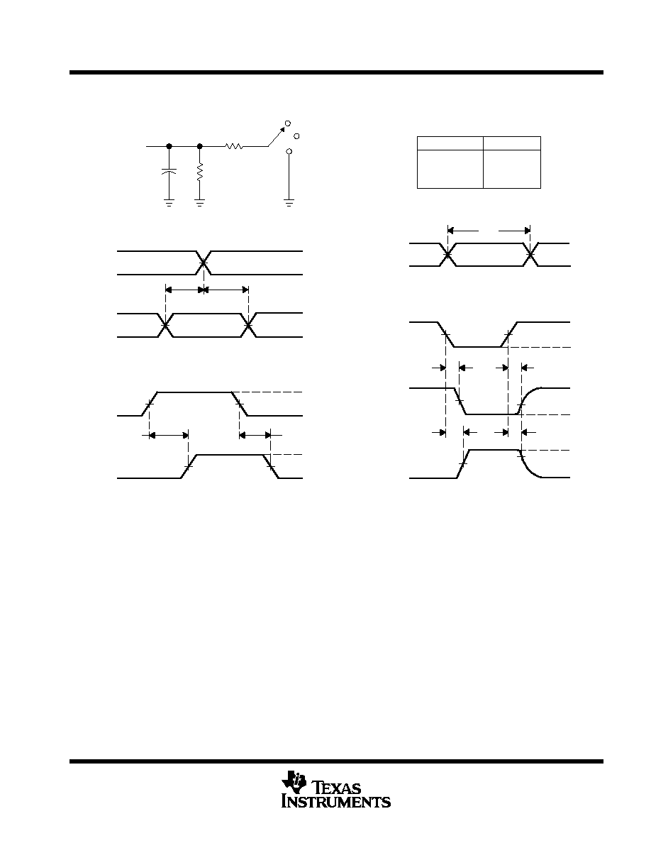
PARAMETER MEASUREMENT INFORMATION
V
CC
= 1.5 V
VCC/2
VCC/2
VCC/2
VCC/2
VCC/2
VCC/2
VCC/2
VCC/2
VOH
VOL
th
tsu
From Output
Under Test
CL = 15 pF
(see Note A)
LOAD CIRCUIT
S1
Open
GND
2 k
2 k
Output
Control
(low-level
enabling)
Output
Waveform 1
S1 at 2
◊
VCC
(see Note B)
Output
Waveform 2
S1 at GND
(see Note B)
tPZL
tPZH
tPLZ
tPHZ
0 V
VOL + 0.1 V
VOH ≠ 0.1 V
0 V
VCC
0 V
0 V
tw
VCC
VCC
VOLTAGE WAVEFORMS
SETUP AND HOLD TIMES
VOLTAGE WAVEFORMS
PULSE DURATION
VOLTAGE WAVEFORMS
ENABLE AND DISABLE TIMES
Timing
Input
Data
Input
Input
tpd
tPLZ/tPZL
tPHZ/tPZH
Open
2
◊
VCC
GND
TEST
S1
NOTES: A. CL includes probe and jig capacitance.
B. Waveform 1 is for an output with internal conditions such that the output is low except when disabled by the output control.
Waveform 2 is for an output with internal conditions such that the output is high except when disabled by the output control.
C. All input pulses are supplied by generators having the following characteristics: PRR
10 MHz, ZO = 50
, tr
2 ns, tf
2 ns.
D. The outputs are measured one at a time with one transition per measurement.
E. tPLZ and tPHZ are the same as tdis.
F. tPZL and tPZH are the same as ten.
G. tPLH and tPHL are the same as tpd.
0 V
VCC
VCC/2
tPHL
VCC/2
VCC/2
VCC
0 V
VOH
VOL
Input
Output
VOLTAGE WAVEFORMS
PROPAGATION DELAY TIMES
VCC/2
VCC/2
tPLH
2
◊
VCC
VCC
Figure 1. Load Circuit and Voltage Waveforms