Äîêóìåíòàöèÿ è îïèñàíèÿ www.docs.chipfind.ru
SN74LVC2G241
DUAL BUFFER/DRIVER
WITH 3 STATE OUTPUTS
SCES210K - APRIL 1999 - REVISED OCTOBER 2003
1
POST OFFICE BOX 655303
·
DALLAS, TEXAS 75265
D
Available in the Texas Instruments
NanoStar
and NanoFree
Packages
D
Supports 5-V V
CC
Operation
D
Inputs Accept Voltages to 5.5 V
D
Max t
pd
of 4.1 ns at 3.3 V
D
Low Power Consumption, 10-
µ
A Max I
CC
D
±
24-mA Output Drive at 3.3 V
D
Typical V
OLP
(Output Ground Bounce)
<0.8 V at V
CC
= 3.3 V, T
A
= 25
°
C
D
Typical V
OHV
(Output V
OH
Undershoot)
>2 V at V
CC
= 3.3 V, T
A
= 25
°
C
D
I
off
Supports Partial-Power-Down Mode
Operation
D
Latch-Up Performance Exceeds 100 mA Per
JESD 78, Class II
D
ESD Protection Exceeds JESD 22
- 2000-V Human-Body Model (A114-A)
- 200-V Machine Model (A115-A)
- 1000-V Charged-Device Model (C101)
description/ordering information
This dual buffer/line driver is designed for 1.65-V to 5.5-V V
CC
operation.
The SN74LVC2G241 is designed specifically to improve both the performance and density of 3-state
memory-address drivers, clock drivers, and bus-oriented receivers and transmitters.
ORDERING INFORMATION
TA
PACKAGE
ORDERABLE
PART NUMBER
TOP-SIDE
MARKING
NanoStar
- WCSP (DSBGA)
0.17-mm Small Bump - YEA
SN74LVC2G241YEAR
NanoFree
- WCSP (DSBGA)
0.17-mm Small Bump - YZA (Pb-free)
Reel of 3000
SN74LVC2G241YZAR
_ _ _C2_
-40
°
C to 85
°
C
NanoStar
- WCSP (DSBGA)
0.23-mm Large Bump - YEP
Reel of 3000
SN74LVC2G241YEPR
_ _ _C2_
-40
°
C to 85
°
C
NanoFree
- WCSP (DSBGA)
0.23-mm Large Bump - YZP (Pb-free)
SN74LVC2G241YZPR
SSOP - DCT
Reel of 3000
SN74LVC2G241DCTR
C41_ _ _
VSSOP - DCU
Reel of 3000
SN74LVC2G241DCUR
C41_
VSSOP - DCU
Reel of 250
SN74LVC2G241DCUT
C41_
Package drawings, standard packing quantities, thermal data, symbolization, and PCB design guidelines are available at
www.ti.com/sc/package.
DCT: The actual top-side marking has three additional characters that designate the year, month, and assembly/test site.
DCU: The actual top-side marking has one additional character that designates the assembly/test site.
YEA/YZA, YEP/YZP: The actual top-side marking has three preceding characters to denote year, month, and sequence code,
and one following character to designate the assembly/test site. Pin 1 identifier indicates solder-bump composition
(1 = SnPb,
·
= Pb-free).
Copyright
2003, Texas Instruments Incorporated
Please be aware that an important notice concerning availability, standard warranty, and use in critical applications of
Texas Instruments semiconductor products and disclaimers thereto appears at the end of this data sheet.
NanoStar and NanoFree are trademarks of Texas Instruments.
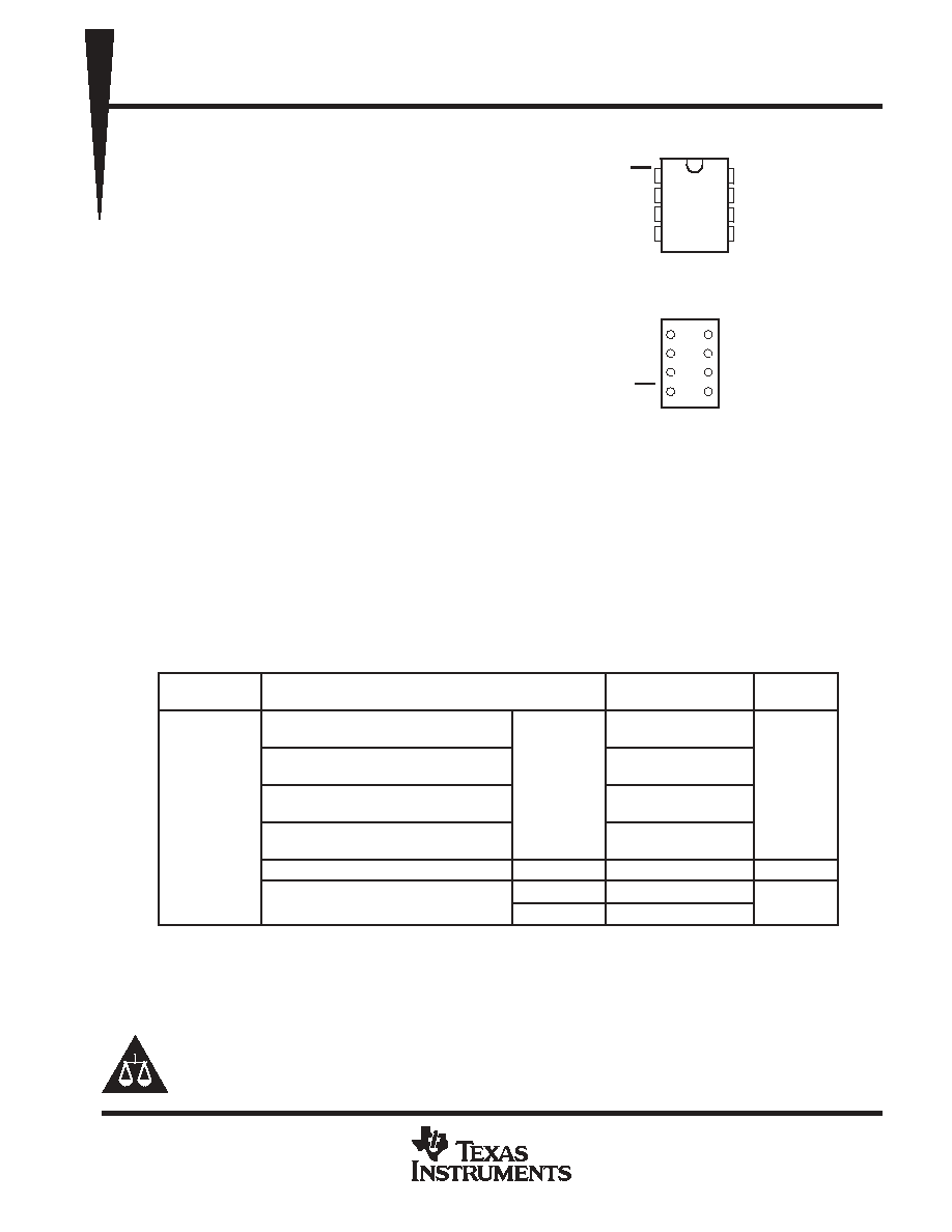
DCT OR DCU PACKAGE
(TOP VIEW)
1
2
3
4
8
7
6
5
1OE
1A
2Y
GND
V
CC
2OE
1Y
2A
4
3
2
1
5
6
7
8
GND
2Y
1A
1OE
2A
1Y
2OE
V
CC
YEA, YEP, YZA, OR YZP PACKAGE
(BOTTOM VIEW)
PRODUCTION DATA information is current as of publication date.
Products conform to specifications per the terms of Texas Instruments
standard warranty. Production processing does not necessarily include
testing of all parameters.
SN74LVC2G241
DUAL BUFFER/DRIVER
WITH 3 STATE OUTPUTS
SCES210K - APRIL 1999 - REVISED OCTOBER 2003
2
POST OFFICE BOX 655303
·
DALLAS, TEXAS 75265
description/ordering information (continued)
NanoStar
and NanoFree
package technology is a major breakthrough in IC packaging concepts, using the
die as the package.
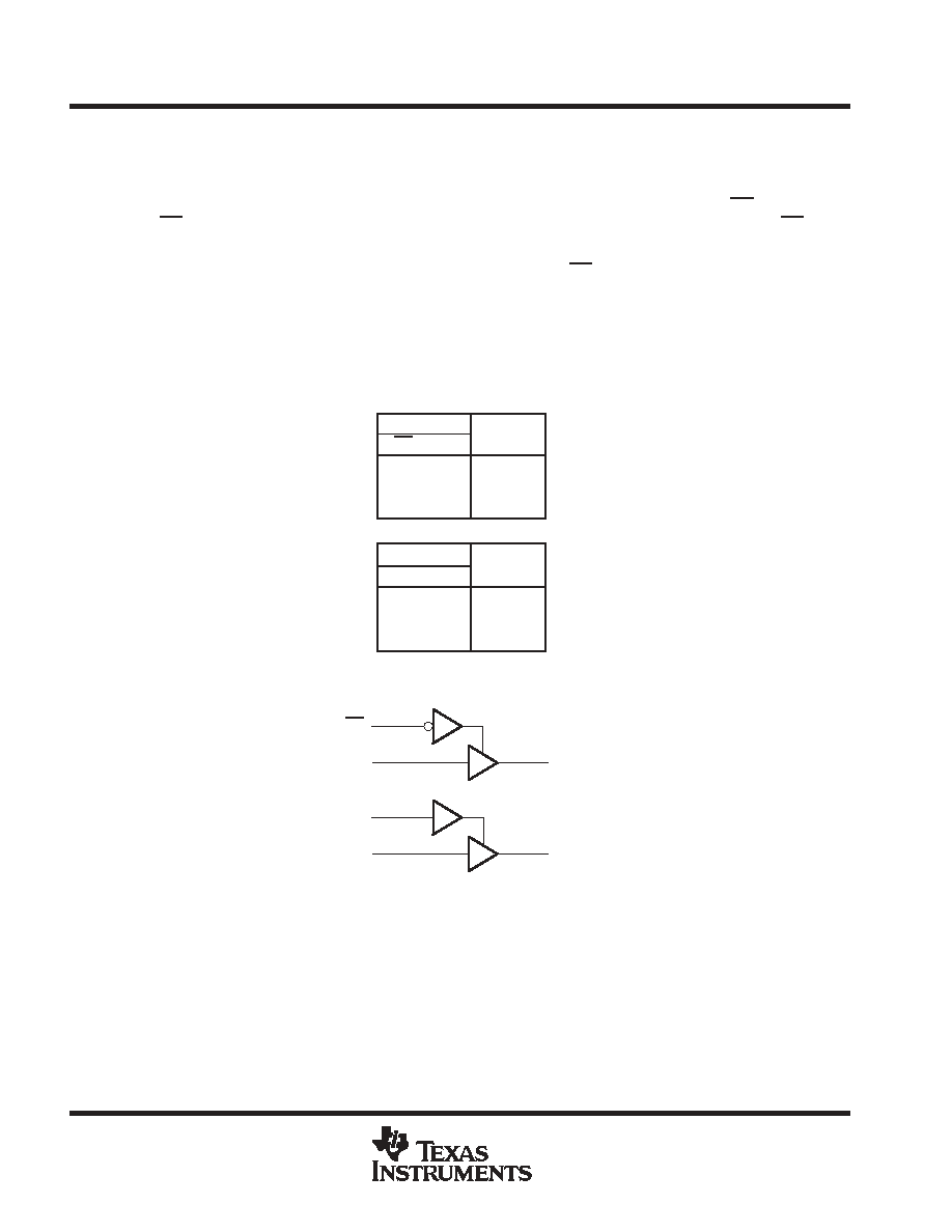
The SN74LVC2G241 is organized as two 1-bit line drivers with separate output-enable (1OE, 2OE) inputs.
When 1OE is low and 2OE is high, the device passes data from the A inputs to the Y outputs. When 1OE is high
and 2OE is low, the outputs are in the high-impedance state.
To ensure the high-impedance state during power up or power down, OE should be tied to V
CC
through a pullup
resistor, and OE should be tied to GND through a pulldown resistor; the minimum value of the resistor is
determined by the current-sinking or the current-sourcing capability of the driver.
This device is fully specified for partial-power-down applications using I
off
. The I
off
circuitry disables the outputs,
preventing damaging current backflow through the device when it is powered down.
Function Tables
INPUTS
OUTPUT
1OE
1A
OUTPUT
1Y
L
H
H
L
L
L
H
X
Z
INPUTS
OUTPUT
2OE
2A
OUTPUT
2Y
H
H
H
H
L
L
L
X
Z
logic diagram (positive logic)
1
2
6
1Y
1OE
1A
7
5
3
2Y
2OE
2A

SN74LVC2G241
DUAL BUFFER/DRIVER
WITH 3 STATE OUTPUTS
SCES210K - APRIL 1999 - REVISED OCTOBER 2003
3
POST OFFICE BOX 655303
·
DALLAS, TEXAS 75265
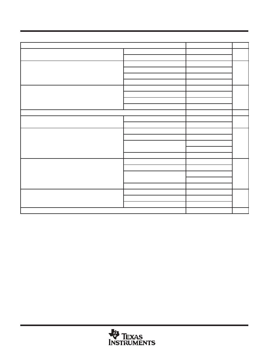
absolute maximum ratings over operating free-air temperature range (unless otherwise noted)
Supply voltage range, V
CC
-0.5 V to 6.5 V
. . . . . . . . . . . . . . . . . . . . . . . . . . . . . . . . . . . . . . . . . . . . . . . . . . . . . . . . .
Input voltage range, V
I
(see Note 1)
-0.5 V to 6.5 V
. . . . . . . . . . . . . . . . . . . . . . . . . . . . . . . . . . . . . . . . . . . . . . . . .
Voltage range applied to any output in the high-impedance or power-off state, V
O
(see Note 1)
-0.5 V to 6.5 V
. . . . . . . . . . . . . . . . . . . . . . . . . . . . . . . . . . . . . . . . . . . . . . . . . . . . . . . . . . . . . . . . . . .
Voltage range applied to any output in the high or low state, V
O
(see Notes 1 and 2)
-0.5 V to V
CC
+ 0.5 V
. . . . . . . . . . . . . . . . . . . . . . . . . . . . . . . . . . . . . . . . . . . . . . . . . . . . . . .
Input clamp current, I
IK
(V
I
< 0 )
-50 mA
. . . . . . . . . . . . . . . . . . . . . . . . . . . . . . . . . . . . . . . . . . . . . . . . . . . . . . . . . .
Output clamp current, I
OK
(V
O
< 0)
-50 mA
. . . . . . . . . . . . . . . . . . . . . . . . . . . . . . . . . . . . . . . . . . . . . . . . . . . . . . . .
Continuous output current, I
O
±
50 mA
. . . . . . . . . . . . . . . . . . . . . . . . . . . . . . . . . . . . . . . . . . . . . . . . . . . . . . . . . . . . .
Continuous current through V
CC
or GND
±
100 mA
. . . . . . . . . . . . . . . . . . . . . . . . . . . . . . . . . . . . . . . . . . . . . . . . . .
Package thermal impedance,
JA
(see Note 3): DCT package
220
°
C/W
. . . . . . . . . . . . . . . . . . . . . . . . . . . . . . .
DCU package
227
°
C/W
. . . . . . . . . . . . . . . . . . . . . . . . . . . . . . .
YEA/YZA package
140
°
C/W
. . . . . . . . . . . . . . . . . . . . . . . . . . .
YEP/YZP package
102
°
C/W
. . . . . . . . . . . . . . . . . . . . . . . . . . .
Storage temperature range, T
stg
-65
°
C to 150
°
C
. . . . . . . . . . . . . . . . . . . . . . . . . . . . . . . . . . . . . . . . . . . . . . . . . . .
Stresses beyond those listed under "absolute maximum ratings" may cause permanent damage to the device. These are stress ratings only, and
functional operation of the device at these or any other conditions beyond those indicated under "recommended operating conditions" is not
implied. Exposure to absolute-maximum-rated conditions for extended periods may affect device reliability.
NOTES:
1. The input negative-voltage and output voltage ratings may be exceeded if the input and output current ratings are observed.
2. The value of VCC is provided in the recommended operating conditions table.
3. The package thermal impedance is calculated in accordance with JESD 51-7.
SN74LVC2G241
DUAL BUFFER/DRIVER
WITH 3 STATE OUTPUTS
SCES210K - APRIL 1999 - REVISED OCTOBER 2003
4
POST OFFICE BOX 655303
·
DALLAS, TEXAS 75265
recommended operating conditions (see Note 4)
MIN
MAX
UNIT
VCC
Supply voltage
Operating
1.65
5.5
V
VCC
Supply voltage
Data retention only
1.5
V
VCC = 1.65 V to 1.95 V
0.65
×
VCC
VIH
High-level input voltage
VCC = 2.3 V to 2.7 V
1.7
V
VIH
High-level input voltage
VCC = 3 V to 3.6 V
2
V
VCC = 4.5 V to 5.5 V
0.7
×
VCC
VCC = 1.65 V to 1.95 V
0.35
×
VCC
VIL
Low-level input voltage
VCC = 2.3 V to 2.7 V
0.7
V
VIL
Low-level input voltage
VCC = 3 V to 3.6 V
0.8
V
VCC = 4.5 V to 5.5 V
0.3
×
VCC
VI
Input voltage
0
5.5
V
VO
Output voltage
High or low state
0
VCC
V
VO
Output voltage
3-state
0
5.5
V
VCC = 1.65 V
-4
VCC = 2.3 V
-8
IOH
High-level output current
VCC = 3 V
-16
mA
IOH
High-level output current
VCC = 3 V
-24
mA
VCC = 4.5 V
-32
VCC = 1.65 V
4
VCC = 2.3 V
8
IOL
Low-level output current
VCC = 3 V
16
mA
IOL
Low-level output current
VCC = 3 V
24
mA
VCC = 4.5 V
32
VCC = 1.8 V
±
0.15 V, 2.5 V
±
0.2 V
20
t/
v
Input transition rise or fall rate
VCC = 3.3 V
±
0.3 V
10
ns/V
t/
v
Input transition rise or fall rate
VCC = 5 V
±
0.5 V
5
ns/V
TA
Operating free-air temperature
-40
85
°
C
NOTE 4: All unused inputs of the device must be held at VCC or GND to ensure proper device operation. Refer to the TI application report,
Implications of Slow or Floating CMOS Inputs, literature number SCBA004.
SN74LVC2G241
DUAL BUFFER/DRIVER
WITH 3 STATE OUTPUTS
SCES210K - APRIL 1999 - REVISED OCTOBER 2003
5
POST OFFICE BOX 655303
·
DALLAS, TEXAS 75265
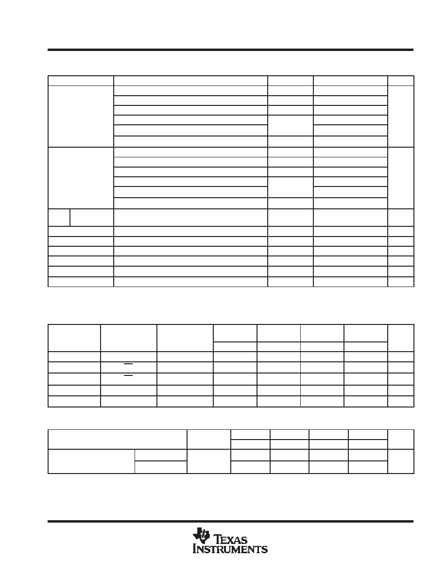
electrical characteristics over recommended operating free-air temperature range (unless
otherwise noted)
PARAMETER
TEST CONDITIONS
VCC
MIN
TYP
MAX
UNIT
IOH = -100
m
A
1.65 V to 5.5 V
VCC-0.1
IOH = -4 mA
1.65 V
1.2
V
IOH = -8 mA
2.3 V
1.9
V
VOH
IOH = -16 mA
3 V
2.4
V
IOH = -24 mA
3 V
2.3
IOH = -32 mA
4.5 V
3.8
IOL = 100
m
A
1.65 V to 5.5 V
0.1
IOL = 4 mA
1.65 V
0.45
V
IOL = 8 mA
2.3 V
0.3
V
VOL
IOL = 16 mA
3 V
0.4
V
IOL = 24 mA
3 V
0.55
IOL = 32 mA
4.5 V
0.55
II
A or Control
inputs
VI = 5.5 V or GND
0 to 5.5 V
±
5
m
A
Ioff
VI or VO = 5.5 V
0
±
10
m
A
IOZ
VO = 0 to 5.5 V
3.6 V
10
m
A
ICC
VI = 5.5 V or GND,
IO = 0
1.65 V to 5.5 V
10
m
A
ICC
One input at VCC - 0.6 V,
Other inputs at VCC or GND
3 V to 5.5 V
500
m
A
Ci
VI = VCC or GND
3.3 V
3.5
pF
Co
VO = VCC or GND
3.3 V
6.5
pF
All typical values are at VCC = 3.3 V, TA = 25
°
C.
switching characteristics over recommended operating free-air temperature range (unless
otherwise noted) (see Figure 1)
PARAMETER
FROM
(INPUT)
TO
(OUTPUT)
VCC = 1.8 V
±
0.15 V
VCC = 2.5 V
±
0.2 V
VCC = 3.3 V
±
0.3 V
VCC = 5 V
±
0.5 V
UNIT
PARAMETER
(INPUT)
(OUTPUT)
MIN
MAX
MIN
MAX
MIN
MAX
MIN
MAX
UNIT
tpd
A
Y
3.3
8.8
1.5
4.8
1.4
4.3
1
3.7
ns
ten
OE
Y
4
9.9
1.9
5.6
1.2
4.7
1.2
3.8
ns
tdis
OE
Y
1.5
11.6
1
5.8
1.4
4.4
1
3.4
ns
ten
OE
Y
3.2
8.8
1.5
4.7
1.6
4.1
1.1
3.3
ns
tdis
OE
Y
1.7
12.5
1
5.2
1
4.2
1
3.3
ns
operating characteristics, T
A
= 25
°
PARAMETER
TEST
VCC = 1.8 V VCC = 2.5 V VCC = 3.3 V
VCC = 5 V
UNIT
PARAMETER
TEST
CONDITIONS
TYP
TYP
TYP
TYP
UNIT
Cpd
Power dissipation
capacitance
Outputs enabled
f = 10 MHz
19
19
20
22
pF
Cpd
capacitance
per buffer/driver
Outputs disabled
f = 10 MHz
2
2
2
3
pF