 | ÐлекÑÑоннÑй компоненÑ: 75C1406 | СкаÑаÑÑ:  PDF PDF  ZIP ZIP |
Äîêóìåíòàöèÿ è îïèñàíèÿ www.docs.chipfind.ru
SN75C1406
TRIPLE LOW-POWER DRIVERS/RECEIVERS
SLLS148D MAY 1990 REVISED DECEMBER 1999
1
POST OFFICE BOX 655303
·
DALLAS, TEXAS 75265
D
Meet or Exceed the Requirements of
TIA/EIA-232-F and ITU Recommendation
V.28
D
Very Low Power Consumption . . .
5 mW Typ
D
Wide Driver Supply Voltage Range . . .
±
4.5 V to
±
15 V
D
Driver Output Slew Rate Limited to
30 V/
µ
s Max
D
Receiver Input Hysteresis . . . 1000 mV Typ
D
Push-Pull Receiver Outputs
D
On-Chip Receiver 1-
µ
s Noise Filter
D
Functionally Interchangeable With Motorola
MC145406 and Texas Instruments
TL145406
D
Package Options Include Plastic
Small-Outline (D, DW, NS) Packages and
(N) DIPs
description
The SN75C1406 is a low-power BiMOS device containing three independent drivers and receivers that are used
to interface data terminal equipment (DTE) with data circuit-terminating equipment (DCE). This device is
designed to conform to TIA/EIA-232-F. The drivers and receivers of the SN75C1406 are similar to those of the
SN75C188 quadruple driver and SN75C189A quadruple receiver, respectively. The drivers have a controlled
output slew rate that is limited to a maximum of 30 V/
µ
s, and the receivers have filters that reject input noise
pulses shorter than 1
µ
s. Both these features eliminate the need for external components.
The SN75C1406 is designed using low-power techniques in a BiMOS technology. In most applications, the
receivers contained in these devices interface to single inputs of peripheral devices such as ACEs, UARTs, or
microprocessors. By using sampling, such peripheral devices are usually insensitive to the transition times of
the input signals. If this is not the case, or for other uses, it is recommended that the SN75C1406 receiver outputs
be buffered by single Schmitt input gates or single gates of the HCMOS, ALS, or 74F logic families.
The SN75C1406 is characterized for operation from 0
°
C to 70
°
C.
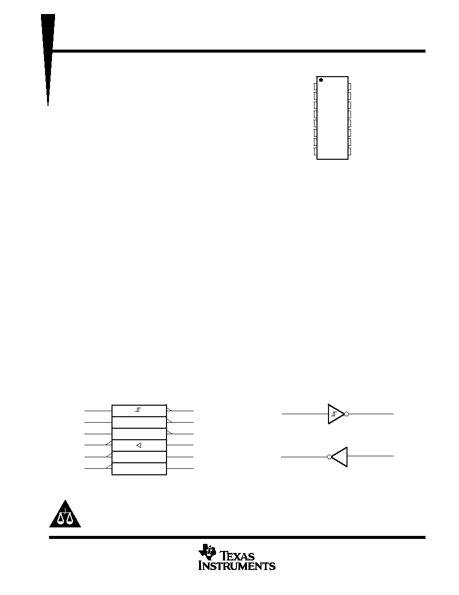
logic symbol
This symbol is in accordance with ANSI/IEEE Std 91-1984 and
IEC Publication 617-12.
1RY
15
2RY
13
3RY
11
1DA
14
2DA
12
3DA
10
1RA
2
2RA
4
3RA
6
1DY
3
2DY
5
3DY
7
logic diagram, each driver and receiver
DY
RA
DA
RY
Copyright
©
1999, Texas Instruments Incorporated
PRODUCTION DATA information is current as of publication date.
Products conform to specifications per the terms of Texas Instruments
standard warranty. Production processing does not necessarily include
testing of all parameters.
Please be aware that an important notice concerning availability, standard warranty, and use in critical applications of
Texas Instruments semiconductor products and disclaimers thereto appears at the end of this data sheet.
1
2
3
4
5
6
7
8
16
15
14
13
12
11
10
9
V
DD
1RA
1DY
2RA
2DY
3RA
3DY
V
SS
V
CC
1RY
1DA
2RY
2DA
3RY
3DA
GND
D, DW, N, OR NS PACKAGE
(TOP VIEW)
SN75C1406
TRIPLE LOW-POWER DRIVERS/RECEIVERS
SLLS148D MAY 1990 REVISED DECEMBER 1999
2
POST OFFICE BOX 655303
·
DALLAS, TEXAS 75265
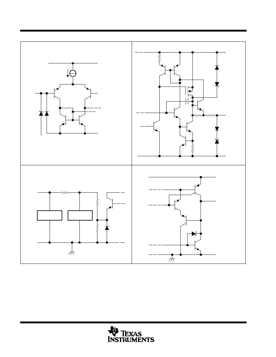
schematics of inputs and outputs
VDD
EQUIVALENT DRIVER INPUT
Internal
1.4-V Reference
VSS
GND
Input
DA
VSS
VDD
Output
DY
160
74
72
GND
530
1.5 k
3.4 k
ESD
Protection
GND
VCC
EQUIVALENT DRIVER OUTPUT
EQUIVALENT RECEIVER INPUT
EQUIVALENT RECEIVER OUTPUT
All resistor values shown are nominal.
Input
RA
Output
RY
ESD
Protection
SN75C1406
TRIPLE LOW-POWER DRIVERS/RECEIVERS
SLLS148D MAY 1990 REVISED DECEMBER 1999
3
POST OFFICE BOX 655303
·
DALLAS, TEXAS 75265
absolute maximum ratings over operating free-air temperature range (unless otherwise noted)
Supply voltage, V
DD
(see Note 1)
15 V
. . . . . . . . . . . . . . . . . . . . . . . . . . . . . . . . . . . . . . . . . . . . . . . . . . . . . . . . . . . .
Supply voltage, V
SS
15 V
. . . . . . . . . . . . . . . . . . . . . . . . . . . . . . . . . . . . . . . . . . . . . . . . . . . . . . . . . . . . . . . . . . . . . . .
Supply voltage, V
CC
7 V
. . . . . . . . . . . . . . . . . . . . . . . . . . . . . . . . . . . . . . . . . . . . . . . . . . . . . . . . . . . . . . . . . . . . . . . .
Input voltage range, V
I
: Driver
V
SS
to V
DD
. . . . . . . . . . . . . . . . . . . . . . . . . . . . . . . . . . . . . . . . . . . . . . . . . . . . . . . . .
Receiver
30 V to 30 V
. . . . . . . . . . . . . . . . . . . . . . . . . . . . . . . . . . . . . . . . . . . . . . . . . . . . .
Output voltage range, V
O
: Driver
(V
SS
6 V) to (V
DD
+ 6 V)
. . . . . . . . . . . . . . . . . . . . . . . . . . . . . . . . . . . . . . . . .
Receiver
0.3 V to (V
CC
+ 0.3 V)
. . . . . . . . . . . . . . . . . . . . . . . . . . . . . . . . . . . . . . . . .
Package thermal impedance,
JA
(see Note 2): D package
73
°
C/W
. . . . . . . . . . . . . . . . . . . . . . . . . . . . . . . . . . .
DW package
57
°
C/W
. . . . . . . . . . . . . . . . . . . . . . . . . . . . . . . . .
N package
67
°
C/W
. . . . . . . . . . . . . . . . . . . . . . . . . . . . . . . . . . .
NS package
64
°
C/W
. . . . . . . . . . . . . . . . . . . . . . . . . . . . . . . . .
Lead temperature 1,6 mm (1/16 inch) from case for 10 seconds
260
°
C
. . . . . . . . . . . . . . . . . . . . . . . . . . . . . . .
Storage temperature range, T
stg
65
°
C to 150
°
C
. . . . . . . . . . . . . . . . . . . . . . . . . . . . . . . . . . . . . . . . . . . . . . . . . .
Stresses beyond those listed under "absolute maximum ratings" may cause permanent damage to the device. These are stress ratings only, and
functional operation of the device at these or any other conditions beyond those indicated under "recommended operating conditions" is not
implied. Exposure to absolute-maximum-rated conditions for extended periods may affect device reliability.
NOTES:
1. All voltages are with respect to the network ground terminal.
2. The package thermal impedance is calculated in accordance with JESD 51.
recommended operating conditions
MIN
NOM
MAX
UNIT
Supply voltage, VDD
4.5
12
15
V
Supply voltage, VSS
4.5
12
15
V
Supply voltage, VCC
4.5
5
6
V
Input voltage VI
Driver
VSS+ 2
VDD
V
Input voltage, VI
Receiver
±
25
V
High-level input voltage, VIH
2
V
Low-level input voltage, VIL
0.8
V
High-level output current, IOH
1
mA
Low-level output current, IOL
3.2
mA
Operating free-air temperature, TA
0
70
°
C
SN75C1406
TRIPLE LOW-POWER DRIVERS/RECEIVERS
SLLS148D MAY 1990 REVISED DECEMBER 1999
4
POST OFFICE BOX 655303
·
DALLAS, TEXAS 75265
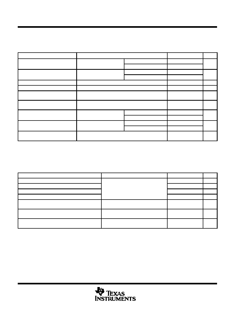
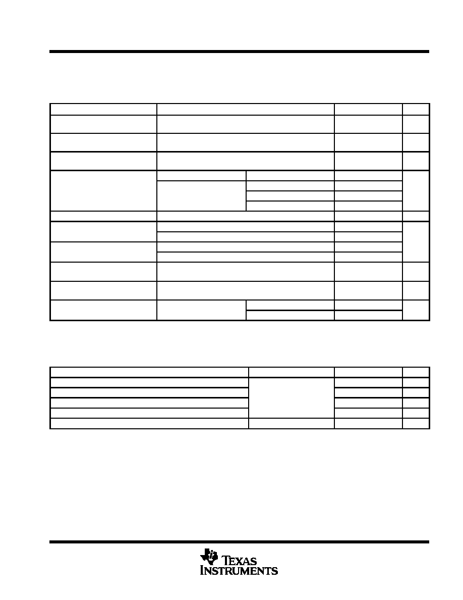
DRIVER SECTION
electrical characteristics over operating free-air temperature range, V
DD
= 12 V, V
SS
= 12 V,
V
CC
= 5 V
±
10% (unless otherwise noted)
PARAMETER
TEST CONDITIONS
MIN
TYP
MAX
UNIT
VOH
High level output voltage
VIH = 0.8 V,
RL = 3 k
,
VDD = 5 V,
VSS = 5 V
4
4.5
V
VOH
High-level output voltage
IH
,
See Figure 1
VDD = 12 V,
VSS = 12 V
10
10.8
V
VOL
Low-level output voltage
VIH = 2 V,
RL = 3 k
,
VDD = 5 V,
VSS = 5 V
4.4
4
V
VOL
g
(see Note 3)
IH
,
See Figure 1
VDD = 12 V,
VSS = 12 V
10.7
10
V
IIH
High-level input current
VI = 5 V,
See Figure 2
1
µ
A
IIL
Low-level input current
VI = 0,
See Figure 2
1
IOS(H)
High-level short-circuit
output current
VI = 0.8 V,
VO = 0 or VSS,
See Figure 1
7.5
12
19.5
mA
IOS(L)
Low-level short-circuit
output current
VI = 2 V,
VO = 0 or VDD,
See Figure 1
7.5
12
19.5
mA
IDD
Supply current from VDD
No load,
VDD = 5 V,
VSS = 5 V
115
250
µ
A
IDD
Supply current from VDD
,
All inputs at 2 V or 0.8 V
VDD = 12 V,
VSS = 12 V
115
250
µ
A
ISS
Supply current from VSS
No load,
VDD = 5 V,
VSS = 5 V
115
250
µ
A
ISS
Supply current from VSS
,
All inputs at 2 V or 0.8 V
VDD = 12 V,
VSS = 12 V
115
250
µ
A
rO
Output resistance
VDD = VSS = VCC = 0,
See Note 4
VO = 2 V to 2 V,
300
400
All typical values are at TA = 25
°
C.
Not more than one output should be shorted at a time.
NOTES:
3. The algebraic convention, where the more positive (less negative) limit is designated as maximum, is used in this data sheet for logic
levels only.
4. Test conditions are those specified by TIA/EIA-232-F.
switching characteristics at T
A
= 25
°
C, V
DD
= 12 V, V
SS
= 12 V, V
CC
= 5 V
±
10%
PARAMETER
TEST CONDITIONS
MIN
TYP
MAX
UNIT
tPLH Propagation delay time, low- to high-level output§
1.2
3
µ
s
tPHL Propagation delay time, high- to low-level output§ RL = 3 k
to 7 k
, CL = 15 pF,
2.5
3.5
µ
s
tTLH Transition time, low- to high-level output¶
L
,
L
,
See Figure 3
0.53
2
3.2
µ
s
tTHL Transition time, high- to low-level output¶
0.53
2
3.2
µ
s
tTLH Transition time, low- to high-level output#
RL = 3 k
to 7 k
, CL = 2500 pF,
See Figure 3
1
2
µ
s
tTHL Transition time, high- to low-level output#
RL = 3 k
to 7 k
, CL = 2500 pF,
See Figure 3
1
2
µ
s
SR
Output slew rate
RL = 3 k
to 7 k
, CL = 15 pF,
See Figure 3
4
10
30
V/
µ
s
§ tPHL and tPLH include the additional time due to on-chip slew rate and are measured at the 50% points.
¶ Measured between 10% and 90% points of output waveform
# Measured between 3-V and 3-V points of output waveform (TIA/EIA-232-F conditions) with all unused inputs tied either high or low
SN75C1406
TRIPLE LOW-POWER DRIVERS/RECEIVERS
SLLS148D MAY 1990 REVISED DECEMBER 1999
5
POST OFFICE BOX 655303
·
DALLAS, TEXAS 75265
RECEIVER SECTION
electrical characteristics over operating free-air temperature range, V
DD
= 12 V, V
SS
= 12 V,
V
CC
= 5 V
±
10% (unless otherwise noted)
PARAMETER
TEST CONDITIONS
MIN
TYP
MAX
UNIT
VIT +
Positive-going input
threshold voltage
See Figure 5
1.7
2
2.55
V
VIT
Negative-going input
threshold voltage
See Figure 5
0.65
1
1.25
V
Vhys
Input hysteresis voltage
(VIT +VIT )
600
1000
mV
VI = 0.75 V,
IOH = 20
µ
A,
See Figure 5 and Note 5
3.5
VOH
High level output voltage
V
0 75 V
I
1
A
VCC = 4.5 V
2.8
4.4
V
VOH
High-level output voltage
VI = 0.75 V,
See Figure 5
IOH = 1 mA,
VCC = 5 V
3.8
4.9
V
See Figure 5
VCC = 5.5 V
4.3
5.4
VOL
Low-level output voltage
VI = 3 V,
IOL = 3.2 mA,
See Figure 5
0.17
0.4
V
IIH
High level input current
VI = 2.5 V
3.6
4.6
8.3
IIH
High-level input current
VI = 3 V
0.43
0.55
1
mA
IIL
Low level input current
VI = 2.5 V
3.6
5
8.3
mA
IIL
Low-level input current
VI = 3 V
0.43
0.55
1
IOS(H)
High-level short-circuit
VI = 0 75 V
VO = 0
See Figure 4
8
15
mA
IOS(H)
g
output current
VI = 0.75 V,
VO = 0,
See Figure 4
8
15
mA
IOS(L)
Low-level short-circuit
VI = VCC
VO = VCC
See Figure 4
13
25
mA
IOS(L)
output current
VI = VCC,
VO = VCC,
See Figure 4
13
25
mA
ICC
Supply current from VCC
No load,
VDD = 5 V,
VSS = 5 V
320
450
µ
A
ICC
Supply current from VCC
All inputs at 0 or 5 V
VDD = 12 V,
VSS = 12 V
320
450
µ
A
All typical values are at TA = 25
°
C.
NOTE 5: If the inputs are left unconnected, the receiver interprets this as an input low and the receiver outputs remain in the high state.
switching characteristics at T
A
= 25
°
C, V
DD
= 12 V, V
SS
= 12 V, V
CC
= 5 V
±
10% (unless otherwise
noted)
PARAMETER
TEST CONDITIONS
MIN
TYP
MAX
UNIT
tPLH Propagation delay time, low- to high-level output
3
4
µ
s
tPHL Propagation delay time, high- to low-level output
CL = 50 pF,
RL = 5 k
,
3
4
µ
s
tTLH
Transition time, low- to high-level output
L
,
See Figure 6
L
,
300
450
ns
tTHL
Transition time, high- to low-level output
100
300
ns
tw(N) Duration of longest pulse rejected as noise§
CL = 50 pF,
RL = 5 k
1
4
µ
s
Measured between 10% and 90% points of output waveform
§ The receiver ignores any positive- or negative-going pulse that is less than the minimum value of tw(N) and accepts any positive- or negative-going
pulse greater than the maximum of tw(N).