 | –≠–ª–µ–∫—Ç—Ä–æ–Ω–Ω—ã–π –∫–æ–º–ø–æ–Ω–µ–Ω—Ç: 7900901CA | –°–∫–∞—á–∞—Ç—å:  PDF PDF  ZIP ZIP |
DS8830, SN55183, SN75183
DUAL DIFFERENTIAL LINE DRIVERS
SLLS093D ≠ OCTOBER 1972 ≠ REVISED APRIL 1998
1
POST OFFICE BOX 655303
∑
DALLAS, TEXAS 75265
D
Single 5-V Supply
D
Differential Line Operation
D
Dual Channels
D
T TL Compatibility
D
Short-Circuit Protection of Outputs
D
Output Clamp Diodes to Terminate Line
Transients
D
High-Current Outputs
D
Quad Inputs
D
Single-Ended or Differential AND/NAND
Outputs
D
Designed for Use With Dual Differential
Drivers SN55182 and SN75182
D
Designed to Be Interchangeable With
National Semiconductor DS7830 and
DS8830
description
The DS8830, SN55183, and SN75183 dual
differential line drivers are designed to provide
differential output signals with high current
capability for driving balanced lines, such as
twisted pair, at normal line impedances without
high power dissipation. These devices can be
used as TTL expander/phase splitters, because
the output stages are similar to TTL totem-pole
outputs.
The driver is of monolithic single-chip construction, and both halves of the dual circuits use common power
supply and ground terminals.
The SN55183 is characterized for operation over the full military temperature range of ≠55
∞
C to 125
∞
C. The
DS8830 and SN75183 are characterized for operation from 0
∞
C to 70
∞
C.
Copyright
©
1998, Texas Instruments Incorporated
PRODUCTION DATA information is current as of publication date.
Products conform to specifications per the terms of Texas Instruments
standard warranty. Production processing does not necessarily include
testing of all parameters.
Please be aware that an important notice concerning availability, standard warranty, and use in critical applications of
Texas Instruments semiconductor products and disclaimers thereto appears at the end of this data sheet.
1
2
3
4
5
6
7
14
13
12
11
10
9
8
1A
1B
1C
1D
1Y
1Z
GND
V
CC
2D
2C
2B
2A
2Y
2Z
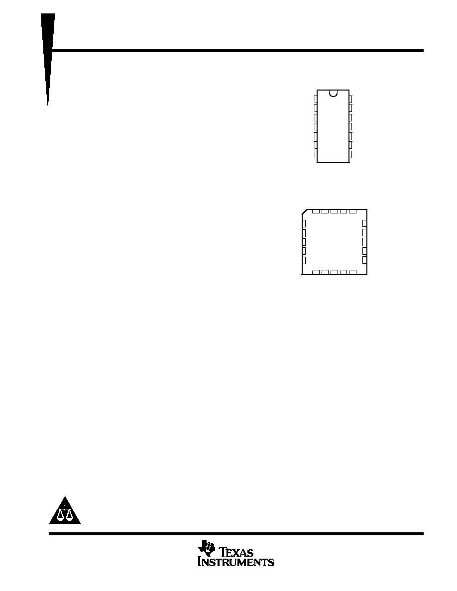
SN55183 . . . J OR W PACKAGE
SN75183 . . . D OR N PACKAGE
DS8830 . . . N PACKAGE
(TOP VIEW)
3
2
1 20 19
9 10 11 12 13
4
5
6
7
8
18
17
16
15
14
2C
NC
2B
NC
2A
1C
NC
1D
NC
1Y
SN55183 . . . FK PACKAGE
(TOP VIEW)
1B
1A
NC
2Z
2Y
2D
1Z
GND
NC
CC
V
THE DS8830 AND SN55183 ARE
NOT RECOMMENDED FOR NEW DESIGNS
NC ≠ No internal connection
DS8830, SN55183, SN75183
DUAL DIFFERENTIAL LINE DRIVERS
SLLS093D ≠ OCTOBER 1972 ≠ REVISED APRIL 1998
2
POST OFFICE BOX 655303
∑
DALLAS, TEXAS 75265
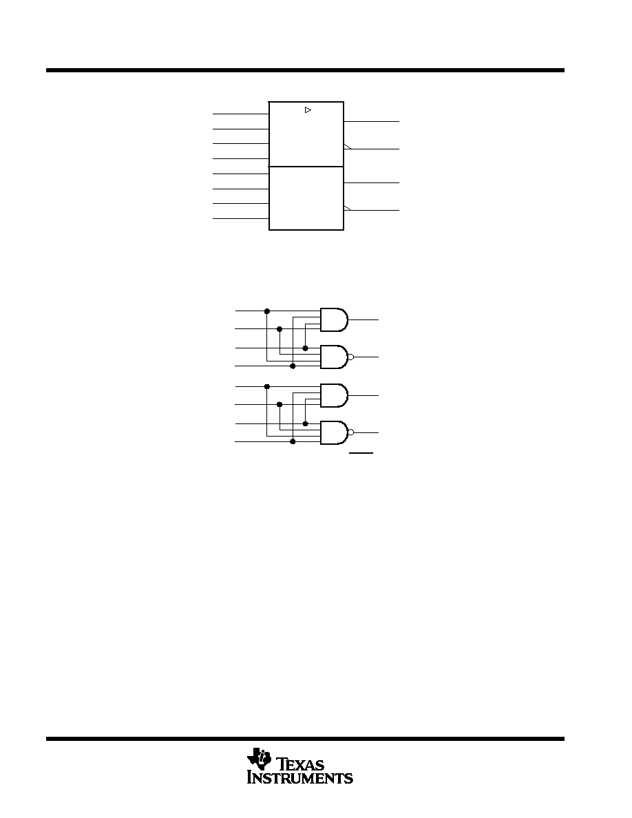
logic symbol
This symbol is in accordance with ANSI/IEEE Std 91-1984 and IEC Publication 617-12.
Pin numbers shown are for the D, J, N, and W packages.
&
1Z
6
2Z
8
1
1A
2
1B
3
1C
4
1D
1Y
5
10
2A
11
2B
12
2C
13
2D
2Y
9
logic diagram (positive logic)
1Y
5
Pin numbers shown are for the D, J, N, and W packages.
1
2
3
4
6
1Z
1A
1B
1C
1D
2Y
9
10
11
12
13
8
2Z
2A
2B
2C
2D
Positive logic: y = ABCD, Z = ABCD
DS8830, SN55183, SN75183
DUAL DIFFERENTIAL LINE DRIVERS
SLLS093D ≠ OCTOBER 1972 ≠ REVISED APRIL 1998
3
POST OFFICE BOX 655303
∑
DALLAS, TEXAS 75265
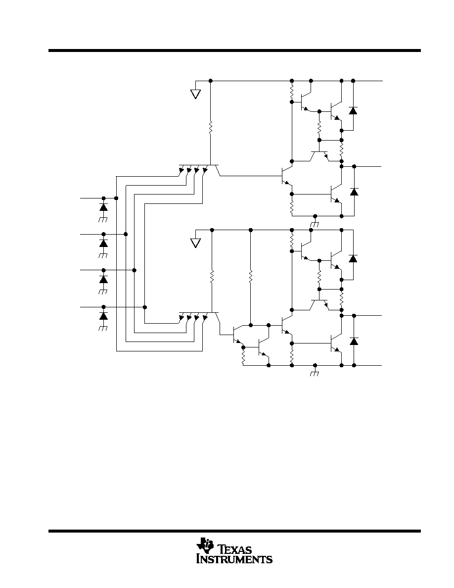
schematic (each driver)
A
B
C
D
4 k
3.2 k
GND
Y
9
300
Z
VCC
3 k
545
2 k
545
3 k
300
2 k
9
V
V
1, 10
14
2, 11
3, 12
4, 13
6, 8
5, 9
7
Resistor values shown are nominal.
Pin numbers shown are for the D, J, N, and W packages.
DS8830, SN55183, SN75183
DUAL DIFFERENTIAL LINE DRIVERS
SLLS093D ≠ OCTOBER 1972 ≠ REVISED APRIL 1998
4
POST OFFICE BOX 655303
∑
DALLAS, TEXAS 75265
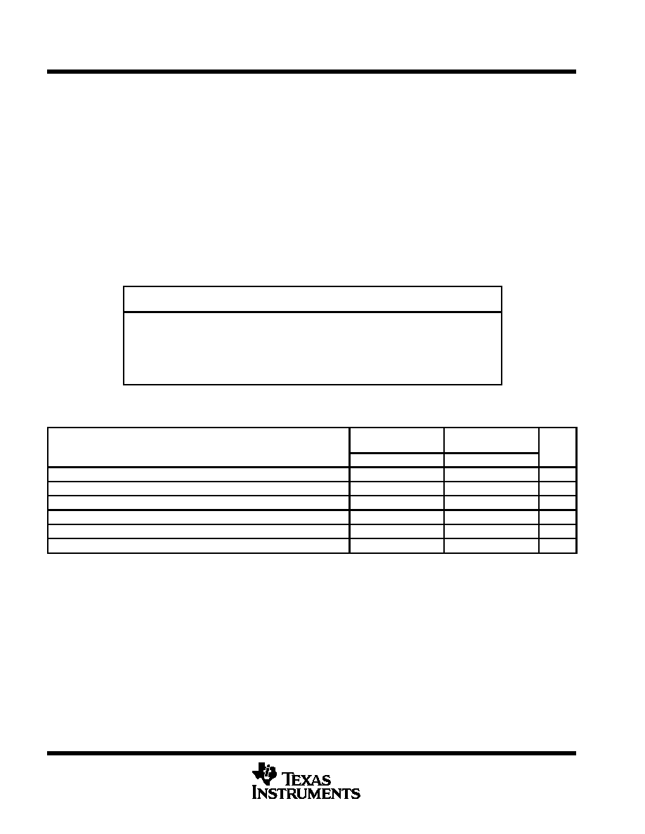
absolute maximum ratings over operating free-air temperature range (unless otherwise noted)
Supply voltage, V
CC
(see Note 1)
7 V
. . . . . . . . . . . . . . . . . . . . . . . . . . . . . . . . . . . . . . . . . . . . . . . . . . . . . . . . . . . . .
Input voltage, V
I
5.5 V
. . . . . . . . . . . . . . . . . . . . . . . . . . . . . . . . . . . . . . . . . . . . . . . . . . . . . . . . . . . . . . . . . . . . . . . . . .
Duration of output short circuit (see Note 2)
1 s
. . . . . . . . . . . . . . . . . . . . . . . . . . . . . . . . . . . . . . . . . . . . . . . . . . . .
Continuous total power dissipation
See Dissipation Rating Table
. . . . . . . . . . . . . . . . . . . . . . . . . . . . . . . . . . . . .
Storage temperature range, T
stg
≠65
∞
C to 150
∞
C
. . . . . . . . . . . . . . . . . . . . . . . . . . . . . . . . . . . . . . . . . . . . . . . . . . .
Lead temperature 1,6 mm (1/16 inch) from case for 10 seconds: D or N package
260
∞
C
. . . . . . . . . . . . . . . .
Lead temperature 1,6 mm (1/16 inch) from case for 60 seconds: J package
300
∞
C
. . . . . . . . . . . . . . . . . . . . .
Case temperature for 60 seconds, T
c
: FK package
260
∞
C
. . . . . . . . . . . . . . . . . . . . . . . . . . . . . . . . . . . . . . . . . . .
Stresses beyond those listed under "absolute maximum ratings" may cause permanent damage to the device. These are stress ratings only, and
functional operation of the device at these or any other conditions beyond those indicated under "recommended operating conditions" is not
implied. Exposure to absolute-maximum-rated conditions for extended periods may affect device reliability.
NOTES:
1. All voltage values, except differential voltages, are with respect to network ground terminal.
2. Not more than one output should be shorted to ground at any one time.
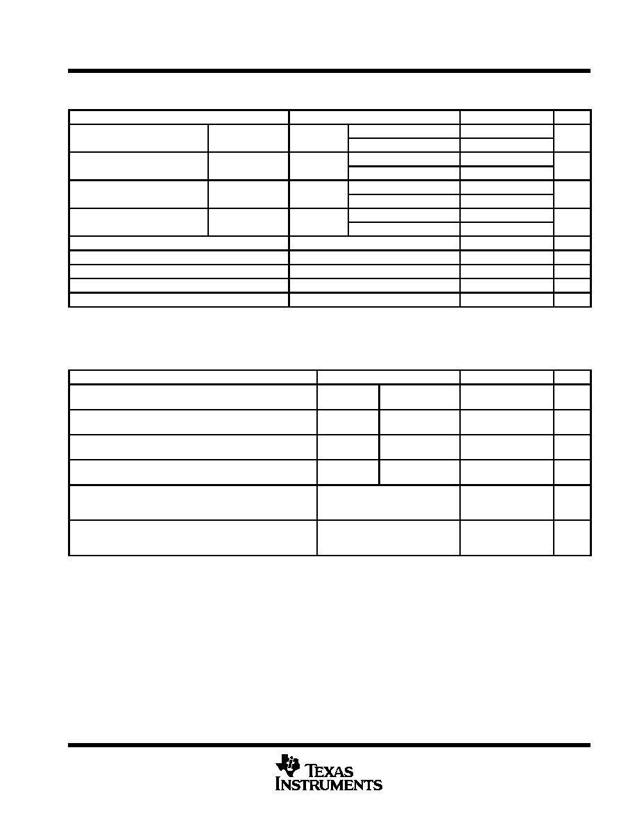
DISSIPATION RATING TABLE
PACKAGE
TA
25
∞
C
POWER RATING
DERATING FACTOR
ABOVE TA = 25
∞
C
TA = 70
∞
C
POWER RATING
TA = 125
∞
C
POWER RATING
D
950 mW
7.6 mW/
∞
C
608 mW
≠
FK
1375 mW
11.0 mW/
∞
C
880 mW
275 mW
J
1375 mW
11.0 mW/
∞
C
880 mW
275 mW
N
1150 mW
9.2 mW/
∞
C
736 mW
≠
W
1000 mW
8.0 mW/
∞
C
640 mW
200 mW
In the FK, J, and W packages, SN55183 chips are alloy mounted and SN75183 chips are glass mounted.
recommended operating conditions
SN55183
DS8830,
SN75183
UNIT
MIN
NOM
MAX
MIN
NOM
MAX
Supply voltage, VCC
4.5
5
5.5
4.75
5
5.25
V
High-level input voltage, VIH
2
2
V
Low-level input voltage, VIL
0.8
0.8
V
High-level output current, IOH
≠40
≠40
mA
Low-level output current, IOL
40
40
mA
Operating free-air temperature, TA
≠55
125
0
70
∞
C
DS8830, SN55183, SN75183
DUAL DIFFERENTIAL LINE DRIVERS
SLLS093D ≠ OCTOBER 1972 ≠ REVISED APRIL 1998
5
POST OFFICE BOX 655303
∑
DALLAS, TEXAS 75265
electrical characteristics over recommended ranges of V
CC
and operating free-air temperature
(unless otherwise noted)
PARAMETER
TEST CONDITIONS
MIN
TYP
MAX
UNIT
VOH
High level output voltage
Y (AND) outputs
VIH = 2 V
IOH = ≠0.8 mA
2.4
V
VOH
High-level output voltage
Y (AND) outputs
VIH = 2 V
IOH = ≠40 mA
1.8
3.3
V
VOL
Low level output voltage
Y (AND) outputs
VIL = 0 8 V
IOL = 32 mA
0.2
V
VOL
Low-level output voltage
Y (AND) outputs
VIL = 0.8 V
IOL = 40 mA
0.22
0.4
V
VOH
High level output voltage
Z (NAND) outputs
VIL = 0 8 V
IOH = ≠0.8 mA
2.4
V
VOH
High-level output voltage
Z (NAND) outputs
VIL = 0.8 V
IOH = ≠40 mA
1.8
3.3
V
VOL
Low level output voltage
Z (NAND) outputs
VIH = 2 V
IOL = 32 mA
0.2
V
VOL
Low-level output voltage
Z (NAND) outputs
VIH = 2 V
IOL = 40 mA
0.22
0.4
V
IIH
High-level input current
VIH = 2.4 V
120
µ
A
II
Input current at maximum input voltage
VIH = 5.5 V
2
mA
IIL
Low-level input current
VIL = 0.4 V
≠4.8
mA
IOS
Short-circuit output current
VCC = 5 V,
TA =125
∞
Cß
≠40
≠100
≠120
mA
ICC
Supply current (average per driver)
VCC = 5 V,
All inputs at 5 V,
No load
10
18
mA
All typical values are at VCC = 5 V, TA = 25
∞
C.
Not more than one output should be shorted to ground at a time, and duration of the short circuit should not exceed one second.
ß TA = 125
∞
C is applicable to SN55183 only.
switching characteristics, V
CC
= 5 V, T
A
= 25
∞
C
PARAMETER
TEST CONDITIONS
MIN
TYP
MAX
UNIT
tPLH
Propagation delay time, low- to high-level Y output
AND gates
CL = 15 pF,
See FIgure 1(a)
8
12
ns
tPHL
Propagation delay time, high- to low-level Y output
AND gates
CL = 15 pF,
See FIgure 1(a)
12
18
ns
tPLH
Propagation delay time, low- to high-level Z output
NAND gates
CL = 15 pF,
See FIgure 1(a)
6
12
ns
tPHL
Propagation delay time, high- to low-level Z output
NAND gates
CL = 15 pF,
See FIgure 1(a)
6
8
ns
tPLH
Propagation delay time,
low- to high-level differential output
Y output with respect to Z output,
RL = 100
in series with 5000 pF,
See Figure 1(b)
9
16
ns
tPHL
Propagation delay time,
high- to low-level differential output
Y output with respect to Z output,
RL = 100
in series with 5000 pF,
See Figure 1(b)
8
16
ns