 | –≠–ª–µ–∫—Ç—Ä–æ–Ω–Ω—ã–π –∫–æ–º–ø–æ–Ω–µ–Ω—Ç: 8302001SA | –°–∫–∞—á–∞—Ç—å:  PDF PDF  ZIP ZIP |

SN54ALS373A, SN54AS373, SN74ALS373A, SN74AS373
OCTAL TRANSPARENT D-TYPE LATCHES
WITH 3-STATE OUTPUTS
SDAS083C ≠ APRIL 1982 ≠ REVISED MARCH 2002
1
POST OFFICE BOX 655303
∑
DALLAS, TEXAS 75265
D
Eight Latches in a Single Package
D
3-State Bus-Driving True Outputs
D
Full Parallel Access for Loading
D
Buffered Control Inputs
D
pnp Inputs Reduce dc Loading on Data
Lines
description
These octal transparent D-type latches feature
3-state outputs designed specifically for driving
highly capacitive or relatively low-impedance
loads. They are particularly suitable for
implementing buffer registers, I/O ports,
bidirectional bus drivers, and working registers.
While the latch-enable (LE) input is high, the Q
outputs follow the data (D) inputs. When LE is
taken low, the Q outputs are latched at the logic
levels set up at the D inputs.
A buffered output-enable (OE) input can be used
to place the eight outputs in either a normal logic
state (high or low) or a high-impedance state. In
the high-impedance state, the outputs neither
load nor drive the bus lines significantly. The
high-impedance state and the increased drive
provide the capability to drive bus lines without
interface or pullup components.
OE does not affect internal operations of the
latches. Old data can be retained or new data can
be entered while the outputs are off.
Copyright
2002, Texas Instruments Incorporated
PRODUCTION DATA information is current as of publication date.
Products conform to specifications per the terms of Texas Instruments
standard warranty. Production processing does not necessarily include
testing of all parameters.
Please be aware that an important notice concerning availability, standard warranty, and use in critical applications of
Texas Instruments semiconductor products and disclaimers thereto appears at the end of this data sheet.
1
2
3
4
5
6
7
8
9
10
20
19
18
17
16
15
14
13
12
11
OE
1Q
1D
2D
2Q
3Q
3D
4D
4Q
GND
V
CC
8Q
8D
7D
7Q
6Q
6D
5D
5Q
LE
SN54ALS373A, . . . J OR W PACKAGE
SN54AS373 . . . J PACKAGE
SN74ALS373A, SN74AS373 . . . DW, N, OR NS PACKAGE
(TOP VIEW)
3
2 1 20 19
9 10 11 12 13
4
5
6
7
8
18
17
16
15
14
8D
7D
7Q
6Q
6D
2D
2Q
3Q
3D
4D
SN54ALS373A, SN54AS373 . . . FK PACKAGE
(TOP VIEW)
1D
1Q
OE
5Q
5D
8Q
4Q
GND
LE
V
CC
On products compliant to MIL-PRF-38535, all parameters are tested
unless otherwise noted. On all other products, production
processing does not necessarily include testing of all parameters.
SN54ALS373A, SN54AS373, SN74ALS373A, SN74AS373
OCTAL TRANSPARENT D-TYPE LATCHES
WITH 3-STATE OUTPUTS
SDAS083C ≠ APRIL 1982 ≠ REVISED MARCH 2002
2
POST OFFICE BOX 655303
∑
DALLAS, TEXAS 75265
ORDERING INFORMATION
TA
PACKAGE
ORDERABLE
PART NUMBER
TOP-SIDE
MARKING
PDIP
N
Tube
SN74ALS373AN
SN74ALS373AN
PDIP ≠ N
Tube
SN74AS373N
SN74AS373N
Tube
SN74ALS373ADW
ALS373A
0
∞
C to 70
∞
C
SOIC
DW
Tape and reel
SN74ALS373ADWR
ALS373A
0
∞
C to 70
∞
C
SOIC ≠ DW
Tube
SN74AS373DW
AS373
Tape and reel
SN74AS373DWR
AS373
SOP
NS
Tape and reel
SN74ALS373ANSR
ALS373A
SOP ≠ NS
Tape and reel
SN74AS373NSR
74AS373
CDIP
J
Tube
SNJ54ALS373AJ
SNJ54ALS373AJ
CDIP ≠ J
Tube
SNJ54AS373J
SNJ54AS373J
≠55
∞
C to 125
∞
C
CFP ≠ W
Tube
SNJ54ALS373AW
SNJ54ALS373AW
LCCC
FK
Tube
SNJ54ALS373AFK
SNJ54ALS373AFK
LCCC ≠ FK
Tube
SNJ54AS373FK
SNJ54AS373FK
Package drawings, standard packing quantities, thermal data, symbolization, and PCB design guidelines
are available at www.ti.com/sc/package.
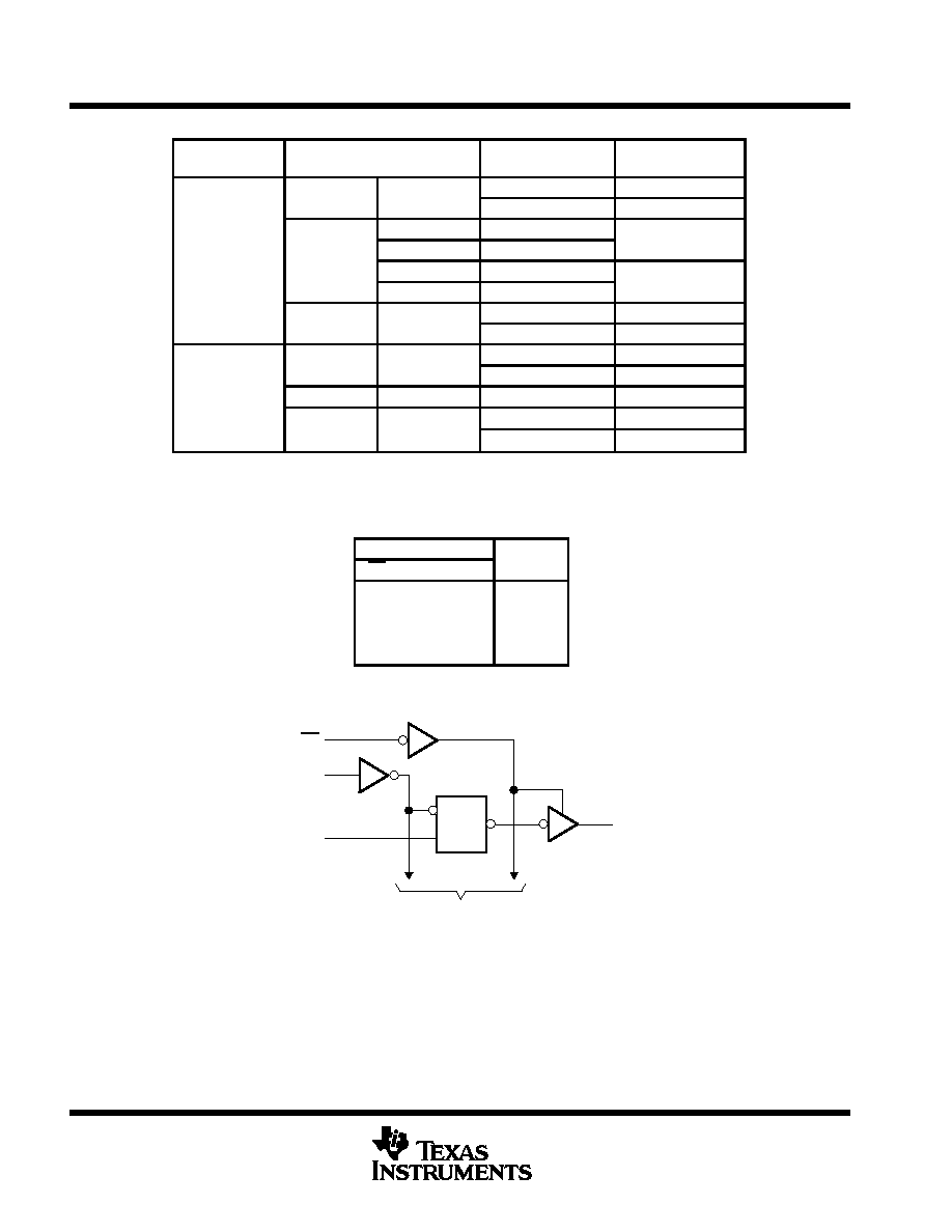
FUNCTION TABLE
(each latch)
INPUTS
OUTPUT
OE
LE
D
Q
L
H
H
H
L
H
L
L
L
L
X
Q0
H
X
X
Z
logic diagram (positive logic)
OE
LE
1D
1Q
1
11
3
2
To Seven Other Channels
C1
1D

SN54ALS373A, SN54AS373, SN74ALS373A, SN74AS373
OCTAL TRANSPARENT D-TYPE LATCHES
WITH 3-STATE OUTPUTS
SDAS083C ≠ APRIL 1982 ≠ REVISED MARCH 2002
3
POST OFFICE BOX 655303
∑
DALLAS, TEXAS 75265
absolute maximum ratings over operating free-air temperature range (SN54ALS373A,
SN74ALS373A) (unless otherwise noted)
Supply voltage, V
CC
7 V
. . . . . . . . . . . . . . . . . . . . . . . . . . . . . . . . . . . . . . . . . . . . . . . . . . . . . . . . . . . . . . . . . . . . . . . .
Input voltage, V
I
7 V
. . . . . . . . . . . . . . . . . . . . . . . . . . . . . . . . . . . . . . . . . . . . . . . . . . . . . . . . . . . . . . . . . . . . . . . . . . . .
Voltage applied to any output in the high state or power-off state
5.5 V
. . . . . . . . . . . . . . . . . . . . . . . . . . . . . . . .
Package thermal impedance,
JA
(see Note 1): DW package
58
∞
C/W
. . . . . . . . . . . . . . . . . . . . . . . . . . . . . . . . .
N package
69
∞
C/W
. . . . . . . . . . . . . . . . . . . . . . . . . . . . . . . . . . .
NS package
60
∞
C/W
. . . . . . . . . . . . . . . . . . . . . . . . . . . . . . . . .
Storage temperature range, T
stg
≠65
∞
C to 150
∞
C
. . . . . . . . . . . . . . . . . . . . . . . . . . . . . . . . . . . . . . . . . . . . . . . . . . .
Stresses beyond those listed under "absolute maximum ratings" may cause permanent damage to the device. These are stress ratings only, and
functional operation of the device at these or any other conditions beyond those indicated under "recommended operating conditions" is not
implied. Exposure to absolute-maximum-rated conditions for extended periods may affect device reliability.
NOTE 1: The package thermal impedance is calculated in accordance with JESD 51-7.
recommended operating conditions
SN54ALS373A
SN74ALS373A
UNIT
MIN
NOM
MAX
MIN
NOM
MAX
UNIT
VCC
Supply voltage
4.5
5
5.5
4.5
5
5.5
V
VIH
High-level input voltage
2
2
V
VIL
Low-level input voltage
0.7
0.8
V
IOH
High-level output current
≠1
≠2.6
mA
IOL
Low-level output current
12
24
mA
TA
Operating free-air temperature
≠55
125
0
70
∞
C
timing requirements over recommended ranges of supply voltage and operating free-air
temperature (unless otherwise noted) (see Figure 1)
SN54ALS373A
SN74ALS373A
UNIT
MIN
MAX
MIN
MAX
UNIT
fclock
Clock frequency
MHz
tw
Pulse duration, LE high
12
10
ns
tsu
Setup time, data before LE
10
10
ns
th
Hold time, data after LE
7
7
ns

SN54ALS373A, SN54AS373, SN74ALS373A, SN74AS373
OCTAL TRANSPARENT D-TYPE LATCHES
WITH 3-STATE OUTPUTS
SDAS083C ≠ APRIL 1982 ≠ REVISED MARCH 2002
4
POST OFFICE BOX 655303
∑
DALLAS, TEXAS 75265
electrical characteristics over recommended operating free-air temperature range (unless
otherwise noted)
PARAMETER
TEST CONDITIONS
SN54ALS373A
SN74ALS373A
UNIT
PARAMETER
TEST CONDITIONS
MIN
TYP
MAX
MIN
TYP
MAX
UNIT
VIK
VCC = 4.5 V,
II = ≠18 mA
≠1.5
≠1.5
V
VCC = 4.5 V to 5.5 V,
IOH = ≠0.4 mA
VCC≠2
VCC≠2
VOH
VCC = 4 5 V
IOH = ≠1 mA
2.4
3.3
V
VCC = 4.5 V
IOH = ≠2.6 mA
2.4
3.2
VOL
VCC = 4 5 V
IOL = 12 mA
0.25
0.4
0.25
0.4
V
VOL
VCC = 4.5 V
IOL = 24 mA
0.35
0.5
V
IOZH
VCC = 5.5 V,
VO = 2.7 V
20
20
µ
A
IOZL
VCC = 5.5 V,
VO = 0.4 V
≠20
≠20
µ
A
II
VCC = 5.5 V,
VI = 7 V
0.1
0.1
mA
IIH
VCC = 5.5 V,
VI = 2.7 V
20
20
µ
A
IIL
VCC = 5.5 V,
VI = 0.4 V
≠0.1
≠0.1
mA
IO
VCC = 5.5 V,
VO = 2.25 V
≠20
≠112
≠30
≠112
mA
Outputs high
9
16
9
16
ICC
VCC = 5.5 V
Outputs low
16
25
16
25
mA
Outputs disabled
17
27
17
27
All typical values are at VCC = 5 V, TA = 25
∞
C.
The output conditions have been chosen to produce a current that closely approximates one-half of the true short-circuit output current, IOS.
switching characteristics (see Figure 1)
PARAMETER
FROM
(INPUT)
TO
(OUTPUT)
VCC = 4.5 V to 5.5 V,
CL = 50 pF,
R1 = 500
,
R2 = 500
,
TA = MIN to MAXß
UNIT
SN54ALS373A
SN74ALS373A
MIN
MAX
MIN
MAX
tPLH
D
Q
2
17
2
12
ns
tPHL
D
Q
1
19
4
16
ns
tPLH
LE
A
Q
6
29
6
22
ns
tPHL
LE
Any Q
1
27
7
23
ns
tPZH
OE
A
Q
6
22
1
18
ns
tPZL
OE
Any Q
5
24
5
20
ns
tPHZ
OE
Any Q
2
16
1
10
ns
tPLZ
OE
Any Q
2
24
2
12
ns
ß For conditions shown as MIN or MAX, use the appropriate value specified under recommended operating conditions.

SN54ALS373A, SN54AS373, SN74ALS373A, SN74AS373
OCTAL TRANSPARENT D-TYPE LATCHES
WITH 3-STATE OUTPUTS
SDAS083C ≠ APRIL 1982 ≠ REVISED MARCH 2002
5
POST OFFICE BOX 655303
∑
DALLAS, TEXAS 75265
absolute maximum ratings over operating free-air temperature range (SN54AS373, SN74AS373)
(unless otherwise noted)
Supply voltage, V
CC
7 V
. . . . . . . . . . . . . . . . . . . . . . . . . . . . . . . . . . . . . . . . . . . . . . . . . . . . . . . . . . . . . . . . . . . . . . . .
Input voltage, V
I
7 V
. . . . . . . . . . . . . . . . . . . . . . . . . . . . . . . . . . . . . . . . . . . . . . . . . . . . . . . . . . . . . . . . . . . . . . . . . . . .
Voltage applied to any output in the high state or power-off state
5.5 V
. . . . . . . . . . . . . . . . . . . . . . . . . . . . . . . .
Package thermal impedance,
JA
(see Note 1): DW package
58
∞
C/W
. . . . . . . . . . . . . . . . . . . . . . . . . . . . . . . . .
N package
69
∞
C/W
. . . . . . . . . . . . . . . . . . . . . . . . . . . . . . . . . . .
NS package
60
∞
C/W
. . . . . . . . . . . . . . . . . . . . . . . . . . . . . . . . .
Storage temperature range, T
stg
≠65
∞
C to 150
∞
C
. . . . . . . . . . . . . . . . . . . . . . . . . . . . . . . . . . . . . . . . . . . . . . . . . . .
Stresses beyond those listed under "absolute maximum ratings" may cause permanent damage to the device. These are stress ratings only, and
functional operation of the device at these or any other conditions beyond those indicated under "recommended operating conditions" is not
implied. Exposure to absolute-maximum-rated conditions for extended periods may affect device reliability.
NOTE 2: The package thermal impedance is calculated in accordance with JESD 51-7.
recommended operating conditions
SN54AS373
SN74AS373
UNIT
MIN
NOM
MAX
MIN
NOM
MAX
UNIT
VCC
Supply voltage
4.5
5
5.5
4.5
5
5.5
V
VIH
High-level input voltage
2
2
V
VIL
Low-level input voltage
0.8
0.8
V
IOH
High-level output current
≠12
≠15
mA
IOL
Low-level output current
32
48
mA
TA
Operating free-air temperature
≠55
125
0
70
∞
C
timing requirements over recommended ranges of supply voltage and operating free-air
temperature (unless otherwise noted) (see Figure 1)
SN54AS373
SN74AS373
UNIT
MIN
MAX
MIN
MAX
UNIT
fclock
Clock frequency
MHz
tw
Pulse duration, LE high
5.5*
4.5*
ns
tsu
Setup time, data before LE
2*
2*
ns
th
Hold time, data after LE
3*
3*
ns
* On products compliant to MIL-STD-883, Class B, this parameter is based on characterization data but is not production tested.