 | –≠–ª–µ–∫—Ç—Ä–æ–Ω–Ω—ã–π –∫–æ–º–ø–æ–Ω–µ–Ω—Ç: 8302502SA | –°–∫–∞—á–∞—Ç—å:  PDF PDF  ZIP ZIP |
SN54ALS569A, SN74ALS568A, SN74ALS569A
SYNCHRONOUS 4-BIT UP/DOWN DECADE AND BINARY COUNTERS
WITH 3-STATE OUTPUTS
SDAS229A ≠ APRIL 1982 ≠ REVISED JANUARY 1995
Copyright
©
1995, Texas Instruments Incorporated
1
POST OFFICE BOX 655303
∑
DALLAS, TEXAS 75265
∑
3-State Q Outputs Drive Bus Lines Directly
∑
Counter Operation Independent of 3-State
Output
∑
Fully Synchronous Clear, Count, and Load
∑
Asynchronous Clear Is Also Provided
∑
Fully Cascadable
∑
Package Options Include Plastic
Small-Outline (DW) Packages, Ceramic
Chip Carriers (FK), and Standard Plastic (N)
and Ceramic (J) 300-mil DIPs
description
The SN74ALS568A decade counter and
ALS569A binary counters are programmable,
count up or down, and offer both synchronous and
asynchronous clearing. All synchronous functions
are executed on the positive-going edge of the
clock (CLK) input.
The clear function is initiated by applying a low
level to either asynchronous clear (ACLR) or
synchronous clear (SCLR). Asynchronous (direct)
clearing overrides all other functions of the device,
while synchronous clearing overrides only the
other synchronous functions. Data is loaded from
the A, B, C, and D inputs by holding load (LOAD)
low during a positive-going clock transition. The
counting function is enabled only when enable P
(ENP) and enable T (ENT) are low and ACLR,
SCLR, and LOAD are high. The up/down (U/D)
input controls the direction of the count. These
counters count up when U/D is high and count
down when U/D is low.
A high level at the output-enable (OE) input forces the Q outputs into the high-impedance state, and a low level
enables those outputs. Counting is independent of OE. ENT is fed forward to enable the ripple-carry output
(RCO) to produce a low-level pulse while the count is zero (all Q outputs low) when counting down or maximum
(9 or 15) when counting up. The clocked carry output (CCO) produces a low-level pulse for a duration equal to
that of the low level of the clock when RCO is low and the counter is enabled (both ENP and ENT are low);
otherwise, CCO is high. CCO does not have the glitches commonly associated with a ripple-carry output.
Cascading is normally accomplished by connecting RCO or CCO of the first counter to ENT of the next counter.
However, for very high-speed counting, RCO should be used for cascading since CCO does not become active
until the clock returns to the low level.
The SN54ALS569A is characterized for operation over the full military temperature range of ≠ 55
∞
C to 125
∞
C.
The SN74ALS568A and SN74ALS569A are characterized for operation from 0
∞
C to 70
∞
C.
1
2
3
4
5
6
7
8
9
10
20
19
18
17
16
15
14
13
12
11
U/D
CLK
A
B
C
D
ENP
ACLR
SCLR
GND
V
CC
RCO
CCO
OE
Q
A
Q
B
Q
C
Q
D
ENT
LOAD
SN54ALS569A . . . J PACKAGE
SN74ALS568A, SN74ALS569A . . . DW OR N PACKAGE
(TOP VIEW)
3
2 1 20 19
9 10 11 12 13
4
5
6
7
8
18
17
16
15
14
CCO
OE
Q
A
Q
B
Q
C
B
C
D
ENP
ACLR
SN54ALS569A . . . FK PACKAGE
(TOP VIEW)
A
CLK
U/D
ENT
Q
RCO
SCLR
GND
LOAD
V
CC
D
PRODUCTION DATA information is current as of publication date.
Products conform to specifications per the terms of Texas Instruments
standard warranty. Production processing does not necessarily include
testing of all parameters.
SN54ALS569A, SN74ALS568A, SN74ALS569A
SYNCHRONOUS 4-BIT UP/DOWN DECADE AND BINARY COUNTERS
WITH 3-STATE OUTPUTS
SDAS229A ≠ APRIL 1982 ≠ REVISED JANUARY 1995
2
POST OFFICE BOX 655303
∑
DALLAS, TEXAS 75265
FUNCTION TABLE
INPUTS
OPERATION
OE
ACLR
SCLR
LOAD
ENT
ENP
U/D
CLK
OPERATION
H
X
X
X
X
X
X
X
Q outputs disabled
L
L
X
X
X
X
X
X
Asynchronous clear
L
H
L
X
X
X
X
Synchronous clear
L
H
H
L
X
X
X
Load
L
H
H
H
L
L
H
Count up
L
H
H
H
L
L
L
Count down
L
H
H
H
H
X
X
X
Inhibit count
L
H
H
H
X
H
X
X
Inhibit count
SN54ALS569A, SN74ALS568A, SN74ALS569A
SYNCHRONOUS 4-BIT UP/DOWN DECADE AND BINARY COUNTERS
WITH 3-STATE OUTPUTS
SDAS229A ≠ APRIL 1982 ≠ REVISED JANUARY 1995
3
POST OFFICE BOX 655303
∑
DALLAS, TEXAS 75265
logic symbols
ENP
CTRDIV10
LOAD
3,5D
3
A
4
B
5
C
6
D
C5/1,4,7,8,+/2,4,7,8≠
19
1,7 (CT=9) G9
10
QA
QB
QC
QD
U/D
ENT
RCO
2,7 (CT=0) G9
18
6,7,8,9
CCO
EN10
17
M2 [DOWN]
M1 [UP]
1
Z6
2
CLK
G7
12
G8
7
5CT=0
9
M4 [COUNT]
M3 [LOAD]
11
CT=0
8
OE
SCLR
ACLR
16
15
14
13
SN74ALS568A
ENP
CTRDIV16
LOAD
3,5D
3
A
4
B
5
C
6
D
C5/1,4,7,8,+/2,4,7,8≠
19
1,7 (CT=15) G9
10
QA
QB
QC
QD
U/D
ENT
RCO
2,7 (CT=0) G9
18
6,7,8,9
CCO
EN10
17
M2 [DOWN]
M1 [UP]
1
Z6
2
CLK
G7
12
G8
7
5CT=0
9
M4 [COUNT]
M3 [LOAD]
11
CT=0
8
OE
SCLR
ACLR
16
15
14
13
ALS569A
These symbols are in accordance with ANSI/IEEE Std 91-1984 and IEC Publication 617-12.
SN54ALS569A, SN74ALS568A, SN74ALS569A
SYNCHRONOUS 4-BIT UP/DOWN DECADE AND BINARY COUNTERS
WITH 3-STATE OUTPUTS
SDAS229A ≠ APRIL 1982 ≠ REVISED JANUARY 1995
4
POST OFFICE BOX 655303
∑
DALLAS, TEXAS 75265
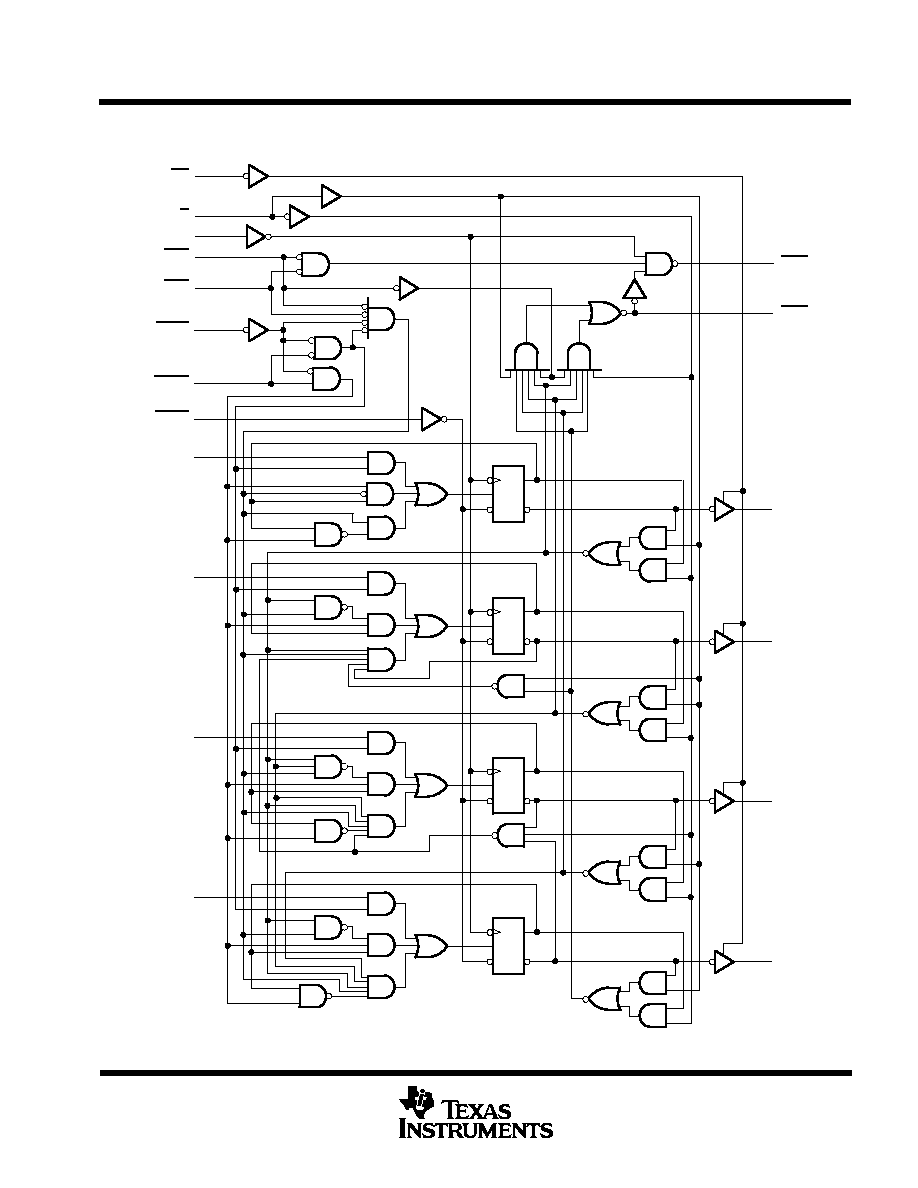
logic diagrams (positive logic)
C1
1D
R
C1
1D
R
C1
1D
R
C1
1D
R
17
1
2
12
9
11
8
3
4
5
6
7
18
19
16
15
14
13
CCO
RCO
QA
QB
QC
QD
OE
U/D
CLK
ENT
ENP
SCLR
LOAD
ACLR
A
B
C
D
SN74ALS568A
SN54ALS569A, SN74ALS568A, SN74ALS569A
SYNCHRONOUS 4-BIT UP/DOWN DECADE AND BINARY COUNTERS
WITH 3-STATE OUTPUTS
SDAS229A ≠ APRIL 1982 ≠ REVISED JANUARY 1995
5
POST OFFICE BOX 655303
∑
DALLAS, TEXAS 75265
logic diagrams (positive logic) (continued)
C1
1D
R
C1
1D
R
C1
1D
R
C1
1D
R
17
1
2
12
9
11
8
3
4
5
6
7
18
19
16
15
14
13
CCO
RCO
QA
QB
QC
QD
OE
U/D
CLK
ENT
ENP
SCLR
LOAD
ACLR
A
B
C
D
ALS569A
SN54ALS569A, SN74ALS568A, SN74ALS569A
SYNCHRONOUS 4-BIT UP/DOWN DECADE AND BINARY COUNTERS
WITH 3-STATE OUTPUTS
SDAS229A ≠ APRIL 1982 ≠ REVISED JANUARY 1995
6
POST OFFICE BOX 655303
∑
DALLAS, TEXAS 75265
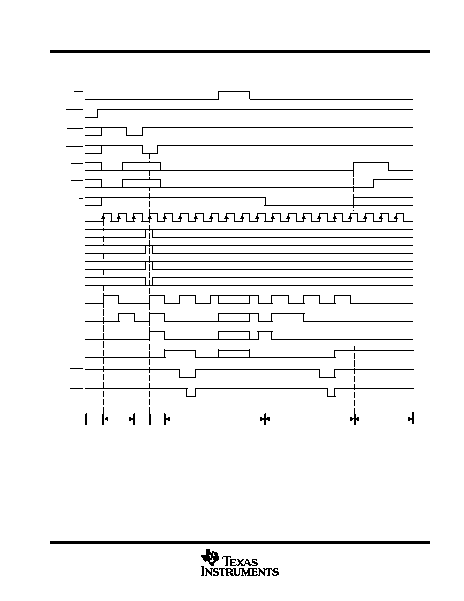
typical load, count, and inhibit sequences
ÃÃÃÃÃÃ
ÃÃÃÃÃÃ
ÃÃÃÃ
ÃÃÃÃ
Hi Z
ÃÃ
ÃÃ
ÃÃÃÃÃÃ
ÃÃÃÃÃÃ
ÃÃÃÃÃÃÃÃÃÃÃÃÃÃÃÃÃÃÃÃÃÃÃ
ÃÃÃÃÃÃÃÃÃÃÃÃÃÃÃÃÃÃÃÃÃÃÃ
LOAD
A
CLK
U/D
ENT
RCO
QA
QB
QC
QD
Async
Clear
1
2
Count Down
Don't Care
Don't Care
ÃÃÃÃÃÃÃÃÃÃÃÃÃÃÃÃÃÃÃÃÃÃÃ
ÃÃÃÃÃÃ
B
Don't Care
Don't Care
ÃÃÃÃÃÃÃÃÃÃÃÃÃÃÃÃÃÃÃÃÃÃÃ
ÃÃÃÃÃÃÃÃÃÃÃÃÃÃÃÃÃÃÃÃÃÃÃ
ÃÃÃÃÃÃ
ÃÃÃÃÃÃ
C
Don't Care
Don't Care
ÃÃÃÃÃÃÃÃÃÃÃÃÃÃÃÃÃÃÃÃÃÃÃ
ÃÃÃÃÃÃÃÃÃÃÃÃÃÃÃÃÃÃÃÃÃÃÃ
ÃÃÃÃÃÃ
ÃÃÃÃÃÃ
D
Don't Care
Don't Care
Don't Care
ÃÃ
ÃÃ
ÃÃÃÃ
ÃÃÃÃ
Don't Care
ENP
ÃÃ
ÃÃ
ÃÃÃÃ
ÃÃÃÃ
Don't Care
ÃÃ
ÃÃ
SCLR
ÃÃ
ÃÃ
ACLR
OE
ÃÃÃÃ
ÃÃÃÃ
Hi Z
ÃÃÃÃ
ÃÃÃÃ
Hi Z
ÃÃÃÃ
Hi Z
CCO
Count Up
Inhibit
Counting
Count
Up
Sync
Clear
Sync
Load
0
7
8
9
0
1
2
3
4
3
2
1
0
9
8
SN74ALS568A

SN54ALS569A, SN74ALS568A, SN74ALS569A
SYNCHRONOUS 4-BIT UP/DOWN DECADE AND BINARY COUNTERS
WITH 3-STATE OUTPUTS
SDAS229A ≠ APRIL 1982 ≠ REVISED JANUARY 1995
7
POST OFFICE BOX 655303
∑
DALLAS, TEXAS 75265
typical load, count, and inhibit sequences (continued)
ÃÃÃÃÃÃ
ÃÃÃÃÃÃ
ÃÃÃÃ
ÃÃÃÃ
Hi Z
ÃÃ
ÃÃ
ÃÃÃÃÃÃ
ÃÃÃÃÃÃ
ÃÃÃÃÃÃÃÃÃÃÃÃÃÃÃÃÃÃÃÃÃÃÃ
ÃÃÃÃÃÃÃÃÃÃÃÃÃÃÃÃÃÃÃÃÃÃÃ
LOAD
A
CLK
U/D
ENT
RCO
QA
QB
QC
QD
Async
Clear
1
2
Count Down
Don't Care
Don't Care
ÃÃÃÃÃÃÃÃÃÃÃÃÃÃÃÃÃÃÃÃÃÃÃ
ÃÃÃÃÃÃ
B
Don't Care
Don't Care
ÃÃÃÃÃÃÃÃÃÃÃÃÃÃÃÃÃÃÃÃÃÃÃ
ÃÃÃÃÃÃÃÃÃÃÃÃÃÃÃÃÃÃÃÃÃÃÃ
ÃÃÃÃÃÃ
ÃÃÃÃÃÃ
C
Don't Care
Don't Care
ÃÃÃÃÃÃÃÃÃÃÃÃÃÃÃÃÃÃÃÃÃÃÃ
ÃÃÃÃÃÃÃÃÃÃÃÃÃÃÃÃÃÃÃÃÃÃÃ
ÃÃÃÃÃÃ
ÃÃÃÃÃÃ
D
Don't Care
Don't Care
Don't Care
ÃÃ
ÃÃ
ÃÃÃÃ
ÃÃÃÃ
Don't Care
ENP
ÃÃ
ÃÃ
ÃÃÃÃ
ÃÃÃÃ
Don't Care
ÃÃ
ÃÃ
SCLR
ÃÃ
ÃÃ
ACLR
OE
ÃÃÃÃ
ÃÃÃÃ
Hi Z
ÃÃÃÃ
ÃÃÃÃ
Hi Z
ÃÃÃÃ
Hi Z
CCO
Count Up
Inhibit
Counting
Count
Up
Sync
Clear
Sync
Load
0
13
14 15
0
1
2
3
4
3
2
1
0
15 14
ALS569A
SN54ALS569A, SN74ALS568A, SN74ALS569A
SYNCHRONOUS 4-BIT UP/DOWN DECADE AND BINARY COUNTERS
WITH 3-STATE OUTPUTS
SDAS229A ≠ APRIL 1982 ≠ REVISED JANUARY 1995
8
POST OFFICE BOX 655303
∑
DALLAS, TEXAS 75265
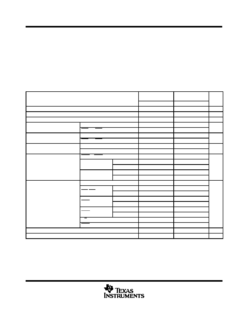
absolute maximum ratings over operating free-air temperature range (unless otherwise noted)
Supply voltage, V
CC
7 V
. . . . . . . . . . . . . . . . . . . . . . . . . . . . . . . . . . . . . . . . . . . . . . . . . . . . . . . . . . . . . . . . . . . . . . . .
Input voltage, V
I
7 V
. . . . . . . . . . . . . . . . . . . . . . . . . . . . . . . . . . . . . . . . . . . . . . . . . . . . . . . . . . . . . . . . . . . . . . . . . . . .
Voltage applied to a disabled 3-state output
5.5 V
. . . . . . . . . . . . . . . . . . . . . . . . . . . . . . . . . . . . . . . . . . . . . . . . . .
Operating free-air temperature range, T
A
: SN54ALS569A
≠ 55
∞
C to 125
∞
C
. . . . . . . . . . . . . . . . . . . . . . . . . . .
SN74ALS568A, SN74ALS569A
0
∞
C to 70
∞
C
. . . . . . . . . . . . . . . . .
Storage temperature range
≠ 65
∞
C to 150
∞
C
. . . . . . . . . . . . . . . . . . . . . . . . . . . . . . . . . . . . . . . . . . . . . . . . . . . . . . .
Stresses beyond those listed under "absolute maximum ratings" may cause permanent damage to the device. These are stress ratings only, and
functional operation of the device at these or any other conditions beyond those indicated under "recommended operating conditions" is not
implied. Exposure to absolute-maximum-rated conditions for extended periods may affect device reliability.
recommended operating conditions
SN54ALS569A
SN74ALS568A
SN74ALS569A
UNIT
MIN
NOM
MAX
MIN
NOM
MAX
VCC
Supply voltage
4.5
5
5.5
4.5
5
5.5
V
VIH
High-level input voltage
2
2
V
VIL
Low-level input voltage
0.7
0.8
V
IOH
High level output current
Q outputs
≠1
≠ 2.6
mA
IOH
High-level output current
CCO and RCO
≠ 0.4
≠ 0.4
mA
IOL
Low level output current
Q outputs
12
24
mA
IOL
Low-level output current
CCO and RCO
4
8
mA
f l k
Clock frequency
SN74ALS568A
0
20
MHz
fclock
Clock frequency
ALS569A
0
22
0
30
MHz
ACLR or LOAD low
20
15
SN74ALS568A
CLK high
25
tw
Pulse duration
SN74ALS568A
CLK low
25
ns
ALS569A
CLK high
20
16.5
ALS569A
CLK low
23
16.5
Data at A, B, C, D
25
20
ENP ENT
High
35
30
ENP, ENT
Low
25
20
SCLR
Low
20
15
tsu
Setup time before CLK
SCLR
High (inactive)
35
30
ns
LOAD
Low
20
15
LOAD
High (inactive)
35
30
U/D
35
30
ACLR inactive
10
10
th
Hold time after CLK
for any input
0
0
ns
TA
Operating free-air temperature
≠ 55
125
0
70
∞
C
SN54ALS569A, SN74ALS568A, SN74ALS569A
SYNCHRONOUS 4-BIT UP/DOWN DECADE AND BINARY COUNTERS
WITH 3-STATE OUTPUTS
SDAS229A ≠ APRIL 1982 ≠ REVISED JANUARY 1995
9
POST OFFICE BOX 655303
∑
DALLAS, TEXAS 75265
electrical characteristics over recommended operating free-air temperature range (unless
otherwise noted)
PARAMETER
TEST CONDITIONS
SN54ALS569A
SN74ALS568A
SN74ALS569A
UNIT
MIN
TYP
MAX
MIN
TYP
MAX
VIK
VCC = 4.5 V,
II = ≠ 18 mA
≠ 1.5
≠ 1.5
V
All outputs
VCC = 4.5 V to 5.5 V,
IOH = ≠ 0.4 mA
VCC ≠ 2
VCC ≠ 2
VOH
Q outputs
VCC = 4 5 V
IOH = ≠ 1 mA
2.4
3.3
V
Q outputs
VCC = 4.5 V
IOH = ≠ 2.6 mA
2.4
3.2
Q outputs
VCC = 4 5 V
IOL = 12 mA
0.25
0.4
0.25
0.4
VOL
Q outputs
VCC = 4.5 V
IOL = 24 mA
0.35
0.5
V
VOL
CCO and RCO
VCC = 4 5 V
IOL = 4 mA
0.25
0.4
0.25
0.4
V
CCO and RCO
VCC = 4.5 V
IOL = 8 mA
0.35
0.5
IOZH
VCC = 5.5 V,
VO = 2.7 V
20
20
µ
A
IOZL
VCC = 5.5 V,
VO = 0.4 V
≠ 20
≠ 20
µ
A
II
VCC = 5.5 V,
VI = 7 V
0.1
0.1
mA
IIH
VCC = 5.5 V,
VI = 2.7 V
20
20
µ
A
IIL
VCC = 5.5 V,
VI = 0.4 V
≠ 0.2
≠ 0.2
mA
IO
CCO and RCO
VCC = 5 5 V
VO = 2 25 V
≠15
≠ 70
≠15
≠ 70
mA
IO
Q outputs
VCC = 5.5 V,
VO = 2.25 V
≠ 20
≠ 112
≠ 30
≠ 112
mA
Outputs high
16
26
16
26
ICC
VCC = 5.5 V
Outputs low
20
32
20
32
mA
Outputs disabled
20
32
20
32
All typical values are at VCC = 5 V, TA = 25
∞
C.
The output conditions have been chosen to produce a current that closely approximates one half of the true short-circuit output current, IOS.
SN54ALS569A, SN74ALS568A, SN74ALS569A
SYNCHRONOUS 4-BIT UP/DOWN DECADE AND BINARY COUNTERS
WITH 3-STATE OUTPUTS
SDAS229A ≠ APRIL 1982 ≠ REVISED JANUARY 1995
10
POST OFFICE BOX 655303
∑
DALLAS, TEXAS 75265
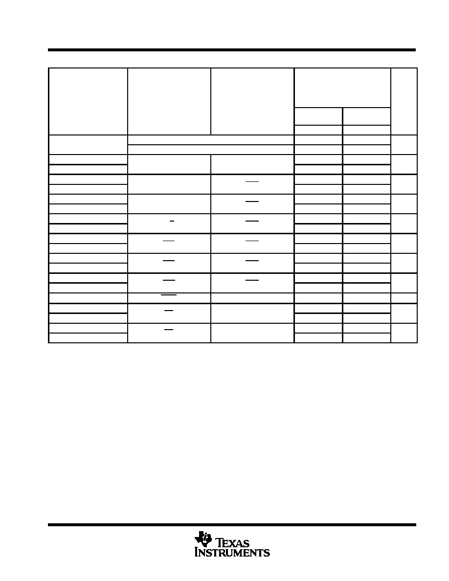
switching characteristics (see Figure 1)
PARAMETER
FROM
(INPUT)
TO
(OUTPUT)
VCC = 4.5 V to 5.5 V,
CL = 50 pF,
R1 = 500
,
R2 = 500
,
TA = MIN to MAX
UNIT
(INPUT)
(OUTPUT)
SN54ALS569A
SN74ALS568A
SN74ALS569A
MIN
MAX
MIN
MAX
f
SN74ALS568A
20
MHz
fmax
ALS569A
22
30
MHz
tPLH
CLK
An Q
4
21
4
13
ns
tPHL
CLK
Any Q
7
19
7
16
ns
tPLH
CLK
RCO
12
37
12
28
ns
tPHL
CLK
RCO
10
28
10
19
ns
tPLH
CLK
CCO
5
17
5
13
ns
tPHL
CLK
CCO
6
30
6
25
ns
tPLH
U/D
RCO
9
31
9
23
ns
tPHL
U/D
RCO
9
33
9
19
ns
tPLH
ENT
RCO
6
21
6
15
ns
tPHL
ENT
RCO
4
20
4
13
ns
tPLH
ENT
CCO
5
18
5
13
ns
tPHL
ENT
CCO
9
32
9
23
ns
tPLH
ENP
CCO
4
18
4
12
ns
tPHL
ENP
CCO
5
18
5
14
ns
tPHL
ACLR
Any Q
9
25
9
20
ns
tPZH
OE
An Q
6
23
6
18
ns
tPZL
OE
Any Q
6
29
6
24
ns
tPHZ
OE
Any Q
1
12
1
10
ns
tPLZ
OE
Any Q
3
29
3
13
ns
For conditions shown as MIN or MAX, use the appropriate value specified under recommended operating conditions.
SN54ALS569A, SN74ALS568A, SN74ALS569A
SYNCHRONOUS 4-BIT UP/DOWN DECADE AND BINARY COUNTERS
WITH 3-STATE OUTPUTS
SDAS229A ≠ APRIL 1982 ≠ REVISED JANUARY 1995
11
POST OFFICE BOX 655303
∑
DALLAS, TEXAS 75265
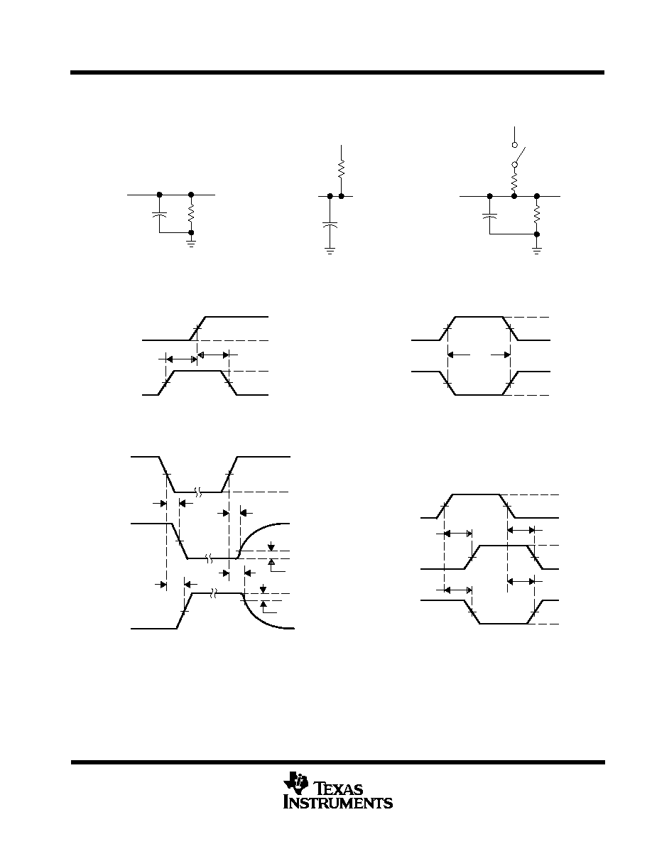
PARAMETER MEASUREMENT INFORMATION
SERIES 54ALS/ 74ALS AND 54AS/ 74AS DEVICES
tPHZ
tPLZ
tPHL
tPLH
0.3 V
tPZL
tPZH
tPLH
tPHL
LOAD CIRCUIT
FOR 3-STATE OUTPUTS
From Output
Under Test
Test
Point
R1
S1
CL
(see Note A)
7 V
1.3 V
1.3 V
1.3 V
3.5 V
3.5 V
0.3 V
0.3 V
th
tsu
VOLTAGE WAVEFORMS
SETUP AND HOLD TIMES
Timing
Input
Data
Input
1.3 V
1.3 V
3.5 V
3.5 V
0.3 V
0.3 V
High-Level
Pulse
Low-Level
Pulse
tw
VOLTAGE WAVEFORMS
PULSE DURATIONS
Input
Out-of-Phase
Output
(see Note C)
1.3 V
1.3 V
1.3 V
1.3 V
1.3 V
1.3 V
1.3 V
1.3 V
1.3 V
1.3 V
3.5 V
3.5 V
0.3 V
0.3 V
VOL
VOH
VOH
VOL
Output
Control
(low-level
enabling)
Waveform 1
S1 Closed
(see Note B)
Waveform 2
S1 Open
(see Note B)
[
0 V
VOH
VOL
[
3.5 V
In-Phase
Output
0.3 V
1.3 V
1.3 V
VOLTAGE WAVEFORMS
PROPAGATION DELAY TIMES
VOLTAGE WAVEFORMS
ENABLE AND DISABLE TIMES, 3-STATE OUTPUTS
R2
VCC
RL
Test
Point
From Output
Under Test
CL
(see Note A)
LOAD CIRCUIT
FOR OPEN-COLLECTOR OUTPUTS
LOAD CIRCUIT FOR
BI-STATE
TOTEM-POLE OUTPUTS
From Output
Under Test
Test
Point
CL
(see Note A)
RL
RL = R1 = R2
NOTES: A. CL includes probe and jig capacitance.
B. Waveform 1 is for an output with internal conditions such that the output is low except when disabled by the output control.
Waveform 2 is for an output with internal conditions such that the output is high except when disabled by the output control.
C. When measuring propagation delay items of 3-state outputs, switch S1 is open.
D. All input pulses have the following characteristics: PRR
1 MHz, tr = tf = 2 ns, duty cycle = 50%.
E. The outputs are measured one at a time with one transition per measurement.
Figure 1. Load Circuits and Voltage Waveforms
PACKAGING INFORMATION
Orderable Device
Status
(1)
Package
Type
Package
Drawing
Pins Package
Qty
Eco Plan
(2)
Lead/Ball Finish
MSL Peak Temp
(3)
83025022A
ACTIVE
LCCC
FK
20
1
TBD
Call TI
Level-NC-NC-NC
8302502RA
ACTIVE
CDIP
J
20
1
TBD
Call TI
Level-NC-NC-NC
8302502SA
ACTIVE
CFP
W
20
1
TBD
Call TI
Level-NC-NC-NC
SN54ALS569AJ
ACTIVE
CDIP
J
20
1
TBD
Call TI
Level-NC-NC-NC
SN74ALS568AN
OBSOLETE
PDIP
N
20
TBD
Call TI
Call TI
SN74ALS569ADW
ACTIVE
SOIC
DW
20
25
Green (RoHS &
no Sb/Br)
CU NIPDAU
Level-1-260C-UNLIM
SN74ALS569ADWE4
ACTIVE
SOIC
DW
20
25
Green (RoHS &
no Sb/Br)
CU NIPDAU
Level-1-260C-UNLIM
SN74ALS569ADWR
ACTIVE
SOIC
DW
20
2000 Green (RoHS &
no Sb/Br)
CU NIPDAU
Level-1-260C-UNLIM
SN74ALS569ADWRE4
ACTIVE
SOIC
DW
20
2000 Green (RoHS &
no Sb/Br)
CU NIPDAU
Level-1-260C-UNLIM
SN74ALS569AN
ACTIVE
PDIP
N
20
20
Pb-Free
(RoHS)
CU NIPDAU
Level-NC-NC-NC
SN74ALS569ANE4
ACTIVE
PDIP
N
20
20
Pb-Free
(RoHS)
CU NIPDAU
Level-NC-NC-NC
SN74ALS569ANSR
ACTIVE
SO
NS
20
2000 Green (RoHS &
no Sb/Br)
CU NIPDAU
Level-1-260C-UNLIM
SN74ALS569ANSRE4
ACTIVE
SO
NS
20
2000 Green (RoHS &
no Sb/Br)
CU NIPDAU
Level-1-260C-UNLIM
SNJ54ALS569AFK
ACTIVE
LCCC
FK
20
1
TBD
Call TI
Level-NC-NC-NC
SNJ54ALS569AJ
ACTIVE
CDIP
J
20
1
TBD
Call TI
Level-NC-NC-NC
SNJ54ALS569AW
ACTIVE
CFP
W
20
1
TBD
Call TI
Level-NC-NC-NC
(1)
The marketing status values are defined as follows:
ACTIVE: Product device recommended for new designs.
LIFEBUY: TI has announced that the device will be discontinued, and a lifetime-buy period is in effect.
NRND: Not recommended for new designs. Device is in production to support existing customers, but TI does not recommend using this part in
a new design.
PREVIEW: Device has been announced but is not in production. Samples may or may not be available.
OBSOLETE: TI has discontinued the production of the device.
(2)
Eco
Plan
-
The
planned
eco-friendly
classification:
Pb-Free
(RoHS)
or
Green
(RoHS
&
no
Sb/Br)
-
please
check
http://www.ti.com/productcontent
for the latest availability information and additional product content details.
TBD: The Pb-Free/Green conversion plan has not been defined.
Pb-Free (RoHS): TI's terms "Lead-Free" or "Pb-Free" mean semiconductor products that are compatible with the current RoHS requirements
for all 6 substances, including the requirement that lead not exceed 0.1% by weight in homogeneous materials. Where designed to be soldered
at high temperatures, TI Pb-Free products are suitable for use in specified lead-free processes.
Green (RoHS & no Sb/Br): TI defines "Green" to mean Pb-Free (RoHS compatible), and free of Bromine (Br) and Antimony (Sb) based flame
retardants (Br or Sb do not exceed 0.1% by weight in homogeneous material)
(3)
MSL, Peak Temp. -- The Moisture Sensitivity Level rating according to the JEDEC industry standard classifications, and peak solder
temperature.
Important Information and Disclaimer:The information provided on this page represents TI's knowledge and belief as of the date that it is
provided. TI bases its knowledge and belief on information provided by third parties, and makes no representation or warranty as to the
accuracy of such information. Efforts are underway to better integrate information from third parties. TI has taken and continues to take
reasonable steps to provide representative and accurate information but may not have conducted destructive testing or chemical analysis on
incoming materials and chemicals. TI and TI suppliers consider certain information to be proprietary, and thus CAS numbers and other limited
information may not be available for release.
PACKAGE OPTION ADDENDUM
www.ti.com
26-Sep-2005
Addendum-Page 1

In no event shall TI's liability arising out of such information exceed the total purchase price of the TI part(s) at issue in this document sold by TI
to Customer on an annual basis.
PACKAGE OPTION ADDENDUM
www.ti.com
26-Sep-2005
Addendum-Page 2
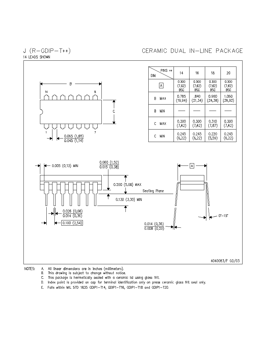
MECHANICAL DATA
MLCC006B ≠ OCTOBER 1996
POST OFFICE BOX 655303
∑
DALLAS, TEXAS 75265
FK (S-CQCC-N**)
LEADLESS CERAMIC CHIP CARRIER
4040140 / D 10/96
28 TERMINAL SHOWN
B
0.358
(9,09)
MAX
(11,63)
0.560
(14,22)
0.560
0.458
0.858
(21,8)
1.063
(27,0)
(14,22)
A
NO. OF
MIN
MAX
0.358
0.660
0.761
0.458
0.342
(8,69)
MIN
(11,23)
(16,26)
0.640
0.739
0.442
(9,09)
(11,63)
(16,76)
0.962
1.165
(23,83)
0.938
(28,99)
1.141
(24,43)
(29,59)
(19,32)
(18,78)
**
20
28
52
44
68
84
0.020 (0,51)
TERMINALS
0.080 (2,03)
0.064 (1,63)
(7,80)
0.307
(10,31)
0.406
(12,58)
0.495
(12,58)
0.495
(21,6)
0.850
(26,6)
1.047
0.045 (1,14)
0.045 (1,14)
0.035 (0,89)
0.035 (0,89)
0.010 (0,25)
12
13
14
15
16
18
17
11
10
8
9
7
5
4
3
2
0.020 (0,51)
0.010 (0,25)
6
1
28
26
27
19
21
B SQ
A SQ
22
23
24
25
20
0.055 (1,40)
0.045 (1,14)
0.028 (0,71)
0.022 (0,54)
0.050 (1,27)
NOTES: A. All linear dimensions are in inches (millimeters).
B. This drawing is subject to change without notice.
C. This package can be hermetically sealed with a metal lid.
D. The terminals are gold plated.
E. Falls within JEDEC MS-004

IMPORTANT NOTICE
Texas Instruments Incorporated and its subsidiaries (TI) reserve the right to make corrections, modifications,
enhancements, improvements, and other changes to its products and services at any time and to discontinue
any product or service without notice. Customers should obtain the latest relevant information before placing
orders and should verify that such information is current and complete. All products are sold subject to TI's terms
and conditions of sale supplied at the time of order acknowledgment.
TI warrants performance of its hardware products to the specifications applicable at the time of sale in
accordance with TI's standard warranty. Testing and other quality control techniques are used to the extent TI
deems necessary to support this warranty. Except where mandated by government requirements, testing of all
parameters of each product is not necessarily performed.
TI assumes no liability for applications assistance or customer product design. Customers are responsible for
their products and applications using TI components. To minimize the risks associated with customer products
and applications, customers should provide adequate design and operating safeguards.
TI does not warrant or represent that any license, either express or implied, is granted under any TI patent right,
copyright, mask work right, or other TI intellectual property right relating to any combination, machine, or process
in which TI products or services are used. Information published by TI regarding third-party products or services
does not constitute a license from TI to use such products or services or a warranty or endorsement thereof.
Use of such information may require a license from a third party under the patents or other intellectual property
of the third party, or a license from TI under the patents or other intellectual property of TI.
Reproduction of information in TI data books or data sheets is permissible only if reproduction is without
alteration and is accompanied by all associated warranties, conditions, limitations, and notices. Reproduction
of this information with alteration is an unfair and deceptive business practice. TI is not responsible or liable for
such altered documentation.
Resale of TI products or services with statements different from or beyond the parameters stated by TI for that
product or service voids all express and any implied warranties for the associated TI product or service and
is an unfair and deceptive business practice. TI is not responsible or liable for any such statements.
Following are URLs where you can obtain information on other Texas Instruments products and application
solutions:
Products
Applications
Amplifiers
amplifier.ti.com
Audio
www.ti.com/audio
Data Converters
dataconverter.ti.com
Automotive
www.ti.com/automotive
DSP
dsp.ti.com
Broadband
www.ti.com/broadband
Interface
interface.ti.com
Digital Control
www.ti.com/digitalcontrol
Logic
logic.ti.com
Military
www.ti.com/military
Power Mgmt
power.ti.com
Optical Networking
www.ti.com/opticalnetwork
Microcontrollers
microcontroller.ti.com
Security
www.ti.com/security
Telephony
www.ti.com/telephony
Video & Imaging
www.ti.com/video
Wireless
www.ti.com/wireless
Mailing Address:
Texas Instruments
Post Office Box 655303 Dallas, Texas 75265
Copyright
2005, Texas Instruments Incorporated