 | –≠–ª–µ–∫—Ç—Ä–æ–Ω–Ω—ã–π –∫–æ–º–ø–æ–Ω–µ–Ω—Ç: 8407101RA | –°–∫–∞—á–∞—Ç—å:  PDF PDF  ZIP ZIP |
1
Data sheet acquired from Harris Semiconductor
SCHS183B
Features
∑ Buffered Inputs
∑ Common Three-State Output Enable Control
∑ Three-State Outputs
∑ Bus Line Driving Capability
∑ Typical Propagation Delay (Clock to Q) = 15ns at
V
CC
= 5V, C
L
= 15pF, T
A
= 25
o
C
∑ Fanout (Over Temperature Range)
- Standard Outputs . . . . . . . . . . . . . . . 10 LSTTL Loads
- Bus Driver Outputs . . . . . . . . . . . . . 15 LSTTL Loads
∑ Wide Operating Temperature Range . . . -55
o
C to 125
o
C
∑ Balanced Propagation Delay and Transition Times
∑ Significant Power Reduction Compared to LSTTL
Logic ICs
∑ HC Types
- 2V to 6V Operation
- High Noise Immunity: N
IL
= 30%, N
IH
= 30% of V
CC
at V
CC
= 5V
∑ HCT Types
- 4.5V to 5.5V Operation
- Direct LSTTL Input Logic Compatibility,
V
IL
= 0.8V (Max), V
IH
= 2V (Min)
- CMOS Input Compatibility, I
l
1
µ
A at V
OL
, V
OH
Description
The 'HC374, 'HCT374, 'HC574, and 'HCT574 are octal D-type
flip-flops with 3-state outputs and the capability to drive 15
LSTTL loads. The eight edge-triggered flip-flops enter data into
their registers on the LOW to HIGH transition of clock (CP). The
output enable (OE) controls the 3-state outputs and is
independent of the register operation. When OE is HIGH, the
outputs are iin the high-impedance state. The 374 and 574 are
identical in function and differ only in their pinout arrangements.
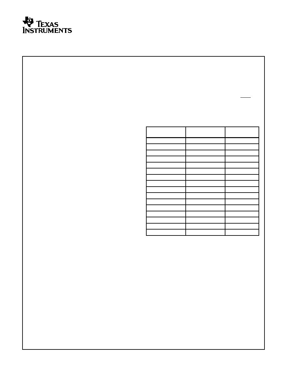
Ordering Information
PART NUMBER
TEMP. RANGE
(
o
C)
PACKAGE
CD54HC374F3A
-55 to 125
20 Ld CERDIP
CD54HC574F3A
-55 to 125
20 Ld CERDIP
CD54HCT374F3A
-55 to 125
20 Ld CERDIP
CD54HCT574F3A
-55 to 125
20 Ld CERDIP
CD74HC374E
-55 to 125
20 Ld PDIP
CD74HC374M
-55 to 125
20 Ld SOIC
CD74HC374M96
-55 to 125
20 Ld SOIC
CD74HC574E
-55 to 125
20 Ld PDIP
CD74HC574M
-55 to 125
20 Ld SOIC
CD74HC574M96
-55 to 125
20 Ld SOIC
CD74HCT374E
-55 to 125
20 Ld PDIP
CD74HCT374M
-55 to 125
20 Ld SOIC
CD74HCT374M96
-55 to 125
20 Ld SOIC
CD74HCT574E
-55 to 125
20 Ld PDIP
CD74HCT574M
-55 to 125
20 Ld SOIC
CD74HCT574M96
-55 to 125
20 Ld SOIC
NOTE: When ordering, use the entire part number. The suffix 96
denotes tape and reel.
February 1998 - Revised May 2003
CAUTION: These devices are sensitive to electrostatic discharge. Users should follow proper IC Handling Procedures.
Copyright
©
2003, Texas Instruments Incorporated
CD54/74HC374, CD54/74HCT374,
CD54/74HC574, CD54/74HCT574
High-Speed CMOS Logic Octal D-Type Flip-Flop,
3-State Positive-Edge Triggered
[ /Title
(CD74
HC374
,
CD74
HCT37
4,
CD74
HC574
,
CD74
HCT57
2
Functional Diagram
Pinouts
CD54HC374, CD54HCT374
(CERDIP)
CD74HC374, CD74HCT374
(PDIP, SOIC)
TOP VIEW
CD54HC574, CD54HCT574
(CERDIP)
CD74HC574, CD74HCT574
(PDIP, SOIC)
TOP VIEW
TRUTH TABLE
INPUTS
OUTPUT
OE
CP
Dn
Qn
L
H
H
L
L
L
L
L
X
Q0
H
X
X
Z
H = High Level (Steady State)
L = Low Level (Steady State)
X= Don't Care
= Transition from Low to High Level
Q0= The level of Q before the indicated steady-state input
conditions were established
Z = High Impedance State
11
12
13
14
15
16
17
18
20
19
10
9
8
7
6
5
4
3
2
1
OE
Q0
D0
D1
Q1
Q2
D3
D2
Q3
GND
V
CC
D7
D6
Q6
Q7
Q5
D5
D4
Q4
CP
11
12
13
14
15
16
17
18
20
19
10
9
8
7
6
5
4
3
2
1
OE
D0
D1
D2
D3
D4
D6
D5
D7
GND
V
CC
Q1
Q2
Q3
Q0
Q4
Q5
Q6
Q7
CP
Q
0
D
0
CP
OE
Q
1
D
1
Q
2
D
2
Q
3
D
3
Q
4
D
4
Q
5
D
5
Q
6
D
6
Q
7
D
7
D
CP Q
D
CP Q
D
CP
Q
D
CP Q
D
CP Q
D
CP Q
D
CP Q
D
CP Q
CD54/74HC374, CD54/74HCT374, CD54/74HC574, CD54/74HCT574
3
Absolute Maximum Ratings
Thermal Information
DC Supply Voltage, V
CC
. . . . . . . . . . . . . . . . . . . . . . . . -0.5V to 7V
DC Input Diode Current, I
IK
For V
I
< -0.5V or V
I
> V
CC
+ 0.5V
. . . . . . . . . . . . . . . . . . . . . .±
20mA
DC Output Diode Current, I
OK
For V
O
< -0.5V or V
O
> V
CC
+ 0.5V
. . . . . . . . . . . . . . . . . . . .±
20mA
DC Drain Current, per Output, I
O
For -0.5V < V
O
< V
CC
+ 0.5V
. . . . . . . . . . . . . . . . . . . . . . . . . .±
35mA
DC Output Source or Sink Current per Output Pin, I
O
For V
O
> -0.5V or V
O
< V
CC
+ 0.5V
. . . . . . . . . . . . . . . . . . . .±
25mA
DC V
CC
or Ground Current, I
CC
. . . . . . . . . . . . . . . . . . . . . . . . .±
50mA
Operating Conditions
Temperature Range, T
A
. . . . . . . . . . . . . . . . . . . . . . -55
o
C to 125
o
C
Supply Voltage Range, V
CC
HC Types . . . . . . . . . . . . . . . . . . . . . . . . . . . . . . . . . . . . .2V to 6V
HCT Types . . . . . . . . . . . . . . . . . . . . . . . . . . . . . . . . .4.5V to 5.5V
DC Input or Output Voltage, V
I
, V
O
. . . . . . . . . . . . . . . . . 0V to V
CC
Input Rise and Fall Time
2V . . . . . . . . . . . . . . . . . . . . . . . . . . . . . . . . . . . . . . 1000ns (Max)
4.5V. . . . . . . . . . . . . . . . . . . . . . . . . . . . . . . . . . . . . . 500ns (Max)
6V . . . . . . . . . . . . . . . . . . . . . . . . . . . . . . . . . . . . . . . 400ns (Max)
Thermal Resistance (Typical, Note 1)
. . . . . . . . . . . . . . . . .
JA
(
o
C/W)
E (PDIP) Package . . . . . . . . . . . . . . . . . . . . . . . . . . . . . . . . . . . 69
M (SOIC) Package. . . . . . . . . . . . . . . . . . . . . . . . . . . . . . . . . . . 58
Maximum Junction Temperature . . . . . . . . . . . . . . . . . . . . . . . 150
o
C
Maximum Storage Temperature Range . . . . . . . . . .-65
o
C to 150
o
C
Maximum Lead Temperature (Soldering 10s) . . . . . . . . . . . . . 300
o
C
(SOIC - Lead Tips Only)
CAUTION: Stresses above those listed in "Absolute Maximum Ratings" may cause permanent damage to the device. This is a stress only rating and operation
of the device at these or any other conditions above those indicated in the operational sections of this specification is not implied.
NOTE:
1. The package thermal impedance is calculated in accordance with JESD 51-7.
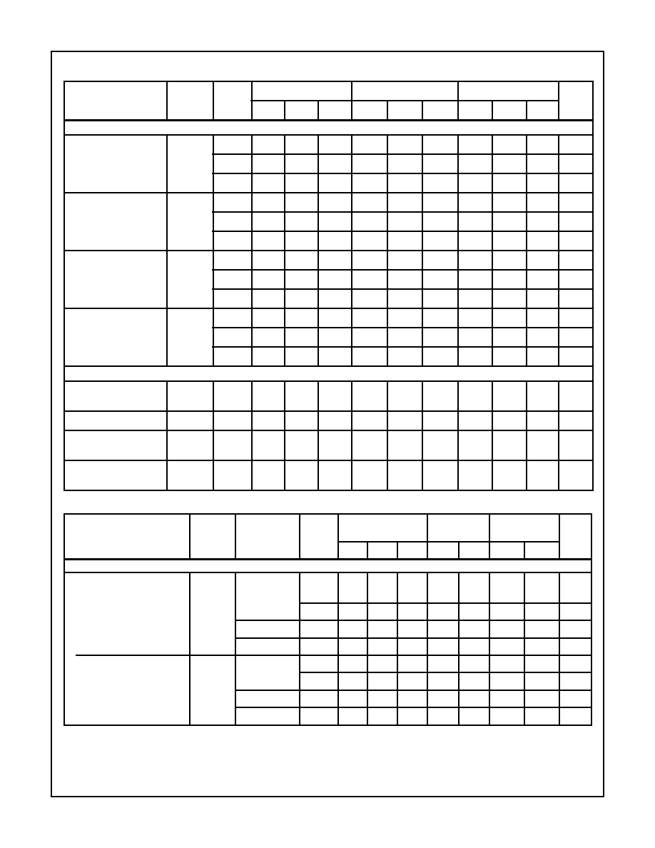
DC Electrical Specifications
PARAMETER
SYMBOL
TEST
CONDITIONS
V
CC
(V)
25
o
C
-40
o
C TO 85
o
C -55
o
C TO 125
o
C
UNITS
V
I
(V)
I
O
(mA)
MIN
TYP
MAX
MIN
MAX
MIN
MAX
HC TYPES
High Level Input
Voltage
V
IH
-
-
2
1.5
-
-
1.5
-
1.5
-
V
4.5
3.15
-
-
3.15
-
3.15
-
V
6
4.2
-
-
4.2
-
4.2
-
V
Low Level Input
Voltage
V
IL
-
-
2
-
-
0.5
-
0.5
-
0.5
V
4.5
-
-
1.35
-
1.35
-
1.35
V
6
-
-
1.8
-
1.8
-
1.8
V
High Level Output
Voltage
CMOS Loads
V
OH
V
IH
or V
IL
-0.02
2
1.9
-
-
1.9
-
1.9
-
V
-0.02
4.5
4.4
-
-
4.4
-
4.4
-
V
-0.02
6
5.9
-
-
5.9
-
5.9
-
V
High Level Output
Voltage
TTL Loads
-
-
-
-
-
-
-
-
-
V
-6
4.5
3.98
-
-
3.84
-
3.7
-
V
-7.8
6
5.48
-
-
5.34
-
5.2
-
V
Low Level Output
Voltage
CMOS Loads
V
OL
V
IH
or V
IL
0.02
2
-
-
0.1
-
0.1
-
0.1
V
0.02
4.5
-
-
0.1
-
0.1
-
0.1
V
0.02
6
-
-
0.1
-
0.1
-
0.1
V
Low Level Output
Voltage
TTL Loads
-
-
-
-
-
-
-
-
-
V
6
4.5
-
-
0.26
-
0.33
-
0.4
V
7.8
6
-
-
0.26
-
0.33
-
0.4
V
Input Leakage
Current
I
I
V
CC
or
GND
-
6
-
-
±
0.1
-
±
1
-
±
1
µ
A
CD54/74HC374, CD54/74HCT374, CD54/74HC574, CD54/74HCT574
4
Quiescent Device
Current
I
CC
V
CC
or
GND
0
6
-
-
8
-
80
-
160
µ
A
Three- State Leakage
Current
V
IL
or V
IH
V
O
= V
CC
or GND
-
6
-
-
±
0.5
-
±
5.0
-
±
10
µ
A
HCT TYPES
High Level Input
Voltage
V
IH
-
-
4.5 to
5.5
2
-
-
2
-
2
-
V
Low Level Input
Voltage
V
IL
-
-
4.5 to
5.5
-
-
0.8
-
0.8
-
0.8
V
High Level Output
Voltage
CMOS Loads
V
OH
V
IH
or V
IL
-0.02
4.5
4.4
-
-
4.4
-
4.4
-
V
High Level Output
Voltage
TTL Loads
-6
4.5
3.98
-
-
3.84
-
3.7
-
V
Low Level Output
Voltage
CMOS Loads
V
OL
V
IH
or V
IL
0.02
4.5
-
-
0.1
-
0.1
-
0.1
V
Low Level Output
Voltage
TTL Loads
6
4.5
-
-
0.26
-
0.33
-
0.4
V
Input Leakage
Current
I
I
V
CC
and
GND
0
5.5
-
±
0.1
-
±
1
-
±
1
µ
A
Quiescent Device
Current
I
CC
V
CC
or
GND
0
5.5
-
-
8
-
80
-
160
µ
A
Three- State Leakage
Current
V
IL
or V
IH
V
O
= V
CC
or GND
-
6
-
-
±
0.5
-
±
5.0
-
±
10
µ
A
Additional Quiescent
Device Current Per
Input Pin: 1 Unit Load
I
CC
(Note 2)
V
CC
-2.1
-
4.5 to
5.5
-
100
360
-
450
-
490
µ
A
NOTE:
2. For dual-supply systems theoretical worst case (V
I
= 2.4V, V
CC
= 5.5V) specification is 1.8mA.
DC Electrical Specifications
(Continued)
PARAMETER
SYMBOL
TEST
CONDITIONS
V
CC
(V)
25
o
C
-40
o
C TO 85
o
C -55
o
C TO 125
o
C
UNITS
V
I
(V)
I
O
(mA)
MIN
TYP
MAX
MIN
MAX
MIN
MAX
HCT Input Loading Table
INPUT
UNIT LOADS
HCT374
HCT574
D0 - D7
0.3
0.4
CP
0.9
0.75
OE
1.3
0.6
NOTE: Unit Load is
I
CC
limit specific in DC Electrical Specifications
Table, e.g., 360
µ
A max. at 25
o
C.
CD54/74HC374, CD54/74HCT374, CD54/74HC574, CD54/74HCT574
5
Prerequisite for Switching Specifications
PARAMETER
SYMBOL
V
CC
(V)
25
o
C
-40
o
C TO 85
o
C
-55
o
C TO 125
o
C
UNITS
MIN
TYP
MAX
MIN
TYP
MAX
MIN
TYP
MAX
HC TYPES
Maximum Clock
Frequency
f
MAX
2
6
-
-
5
-
-
4
-
-
MHz
4.5
30
-
-
25
-
-
20
-
-
MHz
6
35
-
-
29
-
-
23
-
-
MHz
Clock Pulse Width
t
W
2
80
-
-
100
-
-
120
-
-
ns
4.5
16
-
-
20
-
-
24
-
-
ns
6
14
-
-
17
-
-
20
-
-
ns
Setup Time
Data to Clock
t
SU
2
60
-
-
75
-
-
90
-
-
ns
4.5
12
-
-
15
-
-
18
-
-
ns
6
10
-
-
13
-
-
15
-
-
ns
Hold Time
Data to Clock
t
H
2
5
-
-
5
-
-
5
-
-
ns
4.5
5
-
-
5
-
-
5
-
-
ns
6
5
-
-
5
-
-
5
-
-
ns
HCT TYPES
Maximum Clock
Frequency
f
MAX
4.5
30
-
-
25
-
-
20
-
-
MHz
Clock Pulse Width
t
W
4.5
16
-
-
20
-
-
24
-
-
ns
Setup Time
Data to Clock
t
SU
4.5
12
-
-
15
-
-
18
-
-
ns
Hold Time
Data to Clock
t
H
4.5
5
-
-
5
-
-
5
-
-
ns
Switching Specifications
C
L
= 50pF, Input t
r
, t
f
= 6ns
PARAMETER
SYMBOL
TEST
CONDITIONS
V
CC
(V)
25
o
C
-40
o
C TO
85
o
C
-55
o
C TO
125
o
C
UNITS
MIN
TYP
MAX
MIN
MAX
MIN
MAX
HC TYPES
Propagation Delay
t
PLH
, t
PHL
C
L
= 50pF
Clock to Output
2
-
-
165
-
205
-
250
ns
4.5
-
-
33
-
41
-
50
ns
C
L
= 15pF
5
-
15
-
-
-
-
-
ns
C
L
= 50pF
6
-
-
28
-
35
-
43
ns
Output Disable to Q
t
PLZ
, t
PHZ
C
L
= 50pF
2
-
-
135
-
170
-
205
ns
4.5
-
-
27
-
34
-
41
ns
C
L
= 15pF
5
-
11
-
-
-
-
-
ns
C
L
= 50pF
6
-
-
23
-
29
-
35
ns
CD54/74HC374, CD54/74HCT374, CD54/74HC574, CD54/74HCT574
6
Output Enable to Q
t
PZL
, t
PZH
C
L
= 50pF
2
-
-
150
-
190
-
225
ns
4.5
-
-
30
-
38
-
45
ns
C
L
= 15pF
5
-
12
-
-
-
-
-
ns
C
L
= 50pF
6
-
-
26
-
33
-
38
ns
Maximum Clock Frequency
f
MAX
C
L
= 15pF
5
-
60
-
-
-
-
-
MHz
Output Transition Time
t
THL
, t
TLH
C
L
= 50pF
2
-
-
60
-
75
-
90
ns
4.5
-
-
12
-
15
-
18
ns
6
-
-
10
-
13
-
15
ns
Input Capacitance
C
I
C
L
= 50pF
-
10
-
10
-
10
-
10
pF
Three-State Output
Capacitance
C
O
-
-
20
-
20
-
20
-
20
pF
Power Dissipation Capacitance
(Notes 3, 4)
C
PD
C
L
= 15pF
5
-
39
-
-
-
-
-
pF
HCT TYPES
Propagation Delay
t
PHL,
t
PLH
Clock to Output
C
L
= 50pF
4.5
-
-
33
-
41
-
50
ns
C
L
= 15pF
5
-
15
-
-
-
-
-
ns
Output Disable to Q
t
PLZ
, t
PHZ
C
L
= 50pF
4.5
-
-
28
-
35
-
42
ns
C
L
= 15pF
5
-
11
-
-
-
-
-
ns
Output Enable to Q
t
PZL
, t
PZH
C
L
= 50pF
4.5
-
-
30
-
38
-
45
ns
C
L
= 15pF
5
-
12
-
-
-
-
-
ns
Maximum Clock Frequency
f
MAX
C
L
= 15pF
5
-
60
-
-
-
-
-
MHz
Output Transition Time
t
TLH
, t
THL
C
L
= 50pF
4.5
-
-
12
-
15
-
18
ns
Input Capacitance
C
I
C
L
= 50pF
-
10
-
10
-
10
-
10
pF
Three-State Output
Capacitance
C
O
-
-
20
-
20
-
20
-
20
pF
Power Dissipation Capacitance
(Notes 3, 4)
C
PD
C
L
= 15pF
5
-
47
-
-
-
-
-
pF
NOTES:
3. C
PD
is used to determine the dynamic power consumption, per package.
4. P
D
= C
PD
V
CC
2
f
i
+
V
CC
2
f
O
C
L
where f
i
= Input Frequency, f
O
= Output Frequency, C
L
= Output Load Capacitance, V
CC
= Supply
Voltage.
Switching Specifications
C
L
= 50pF, Input t
r
, t
f
= 6ns (Continued)
PARAMETER
SYMBOL
TEST
CONDITIONS
V
CC
(V)
25
o
C
-40
o
C TO
85
o
C
-55
o
C TO
125
o
C
UNITS
MIN
TYP
MAX
MIN
MAX
MIN
MAX
CD54/74HC374, CD54/74HCT374, CD54/74HC574, CD54/74HCT574
7
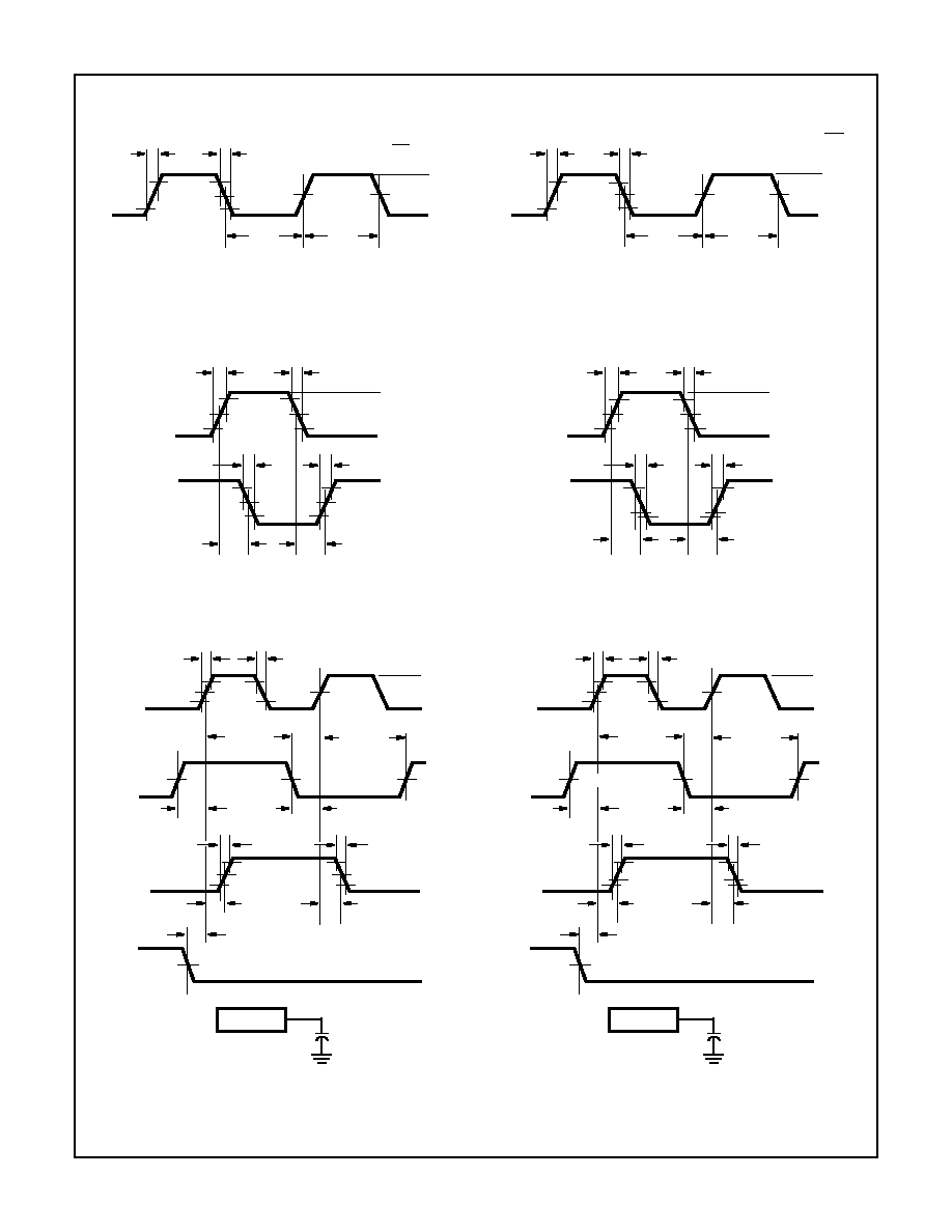
Test Circuits and Waveforms
NOTE: Outputs should be switching from 10% V
CC
to 90% V
CC
in
accordance with device truth table. For f
MAX
, input duty cycle = 50%.
FIGURE 1. HC CLOCK PULSE RISE AND FALL TIMES AND
PULSE WIDTH
NOTE: Outputs should be switching from 10% V
CC
to 90% V
CC
in
accordance with device truth table. For f
MAX
, input duty cycle = 50%.
FIGURE 2. HCT CLOCK PULSE RISE AND FALL TIMES AND
PULSE WIDTH
FIGURE 3. HC TRANSITION TIMES AND PROPAGATION
DELAY TIMES, COMBINATION LOGIC
FIGURE 4. HCT TRANSITION TIMES AND PROPAGATION
DELAY TIMES, COMBINATION LOGIC
FIGURE 5. HC SETUP TIMES, HOLD TIMES, REMOVAL TIME,
AND PROPAGATION DELAY TIMES FOR EDGE
TRIGGERED SEQUENTIAL LOGIC CIRCUITS
FIGURE 6. HCT SETUP TIMES, HOLD TIMES, REMOVAL TIME,
AND PROPAGATION DELAY TIMES FOR EDGE
TRIGGERED SEQUENTIAL LOGIC CIRCUITS
CLOCK
90%
50%
10%
GND
V
CC
t
r
C
L
t
f
C
L
50%
50%
t
WL
t
WH
10%
t
WL
+ t
WH
=
fC
L
I
CLOCK
2.7V
1.3V
0.3V
GND
3V
t
r
C
L
= 6ns
t
f
C
L
= 6ns
1.3V
1.3V
t
WL
t
WH
0.3V
t
WL
+ t
WH
=
fC
L
I
t
PHL
t
PLH
t
THL
t
TLH
90%
50%
10%
50%
10%
INVERTING
OUTPUT
INPUT
GND
V
CC
t
r
= 6ns
t
f
= 6ns
90%
t
PHL
t
PLH
t
THL
t
TLH
2.7V
1.3V
0.3V
1.3V
10%
INVERTING
OUTPUT
INPUT
GND
3V
t
r
= 6ns
t
f
= 6ns
90%
t
r
C
L
t
f
C
L
GND
V
CC
GND
V
CC
50%
90%
10%
GND
CLOCK
INPUT
DATA
INPUT
OUTPUT
SET, RESET
OR PRESET
V
CC
50%
50%
90%
10%
50%
90%
t
REM
t
PLH
t
SU(H)
t
TLH
t
THL
t
H(L)
t
PHL
IC
C
L
50pF
t
SU(L)
t
H(H)
t
r
C
L
t
f
C
L
GND
3V
GND
3V
1.3V
2.7V
0.3V
GND
CLOCK
INPUT
DATA
INPUT
OUTPUT
SET, RESET
OR PRESET
3V
1.3V
1.3V
1.3V
90%
10%
1.3V
90%
t
REM
t
PLH
t
SU(H)
t
TLH
t
THL
t
H(L)
t
PHL
IC
C
L
50pF
t
SU(L)
1.3V
t
H(H)
1.3V
CD54/74HC374, CD54/74HCT374, CD54/74HC574, CD54/74HCT574
8
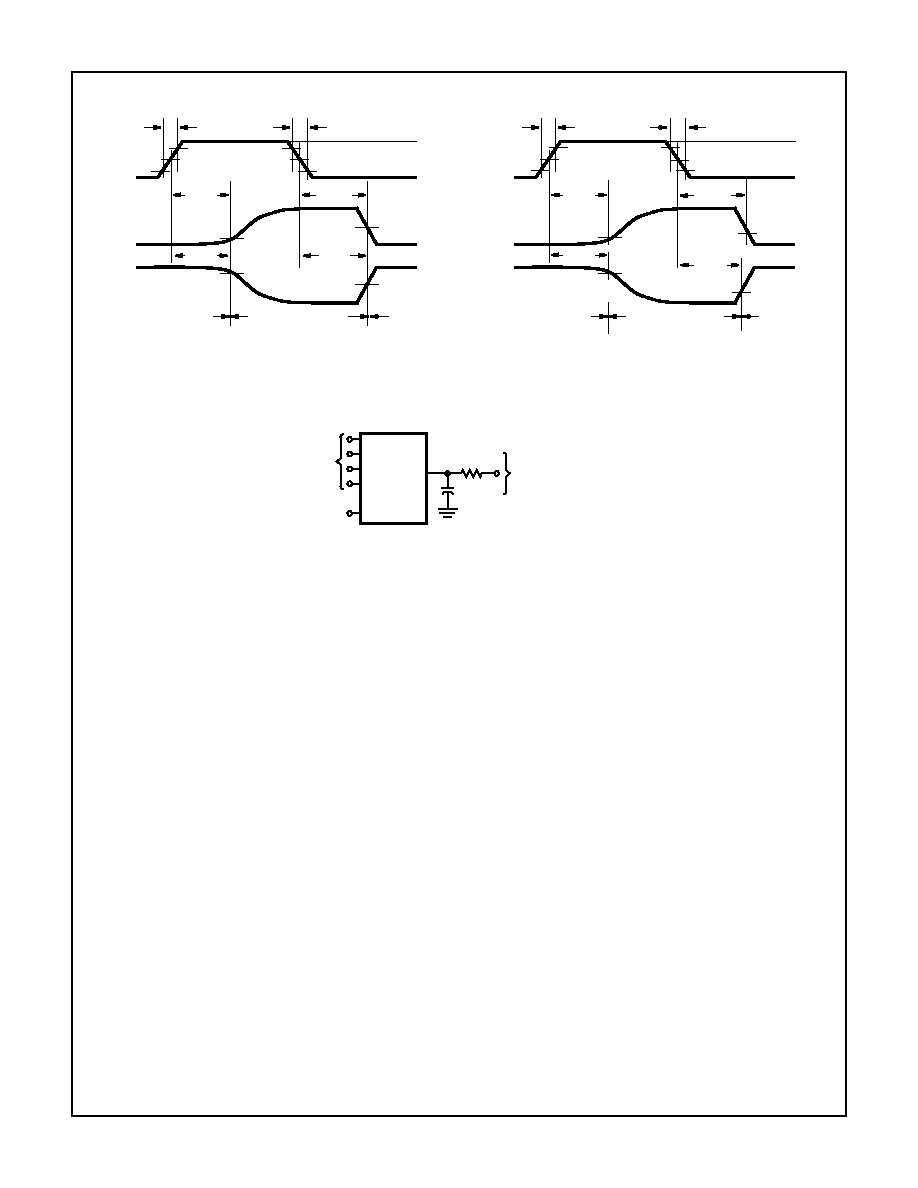
FIGURE 7. HC THREE-STATE PROPAGATION DELAY
WAVEFORM
FIGURE 8. HCT THREE-STATE PROPAGATION DELAY
WAVEFORM
NOTE:
Open drain waveforms t
PLZ
and t
PZL
are the same as those for three-state shown on the left. The test circuit is Output R
L
= 1k
to
V
CC
, C
L
= 50pF.
FIGURE 9. HC AND HCT THREE-STATE PROPAGATION DELAY TEST CIRCUIT
Test Circuits and Waveforms
(Continued)
50%
10%
90%
GND
V
CC
10%
90%
50%
50%
OUTPUT
DISABLE
OUTPUT LOW
TO OFF
OUTPUT HIGH
TO OFF
OUTPUTS
ENABLED
OUTPUTS
DISABLED
OUTPUTS
ENABLED
6ns
6ns
t
PZH
t
PHZ
t
PZL
t
PLZ
0.3
2.7
GND
3V
10%
90%
1.3V
1.3V
OUTPUT
DISABLE
OUTPUT LOW
TO OFF
OUTPUT HIGH
TO OFF
OUTPUTS
ENABLED
OUTPUTS
DISABLED
OUTPUTS
ENABLED
t
r
6ns
t
PZH
t
PHZ
t
PZL
t
PLZ
6ns
t
f
1.3
IC WITH
THREE-
STATE
OUTPUT
OTHER
INPUTS
TIED HIGH
OR LOW
OUTPUT
DISABLE
V
CC
FOR t
PLZ
AND t
PZL
GND FOR t
PHZ
AND t
PZH
OUTPUT
R
L
= 1k
C
L
50pF
CD54/74HC374, CD54/74HCT374, CD54/74HC574, CD54/74HCT574
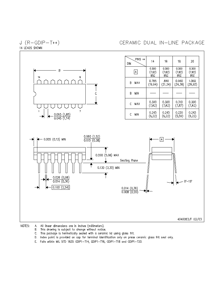
MECHANICAL
MPDI002C ≠ JANUARY 1995 ≠ REVISED DECEMBER 20002
1
POST OFFICE BOX 655303
∑
DALLAS, TEXAS 75265
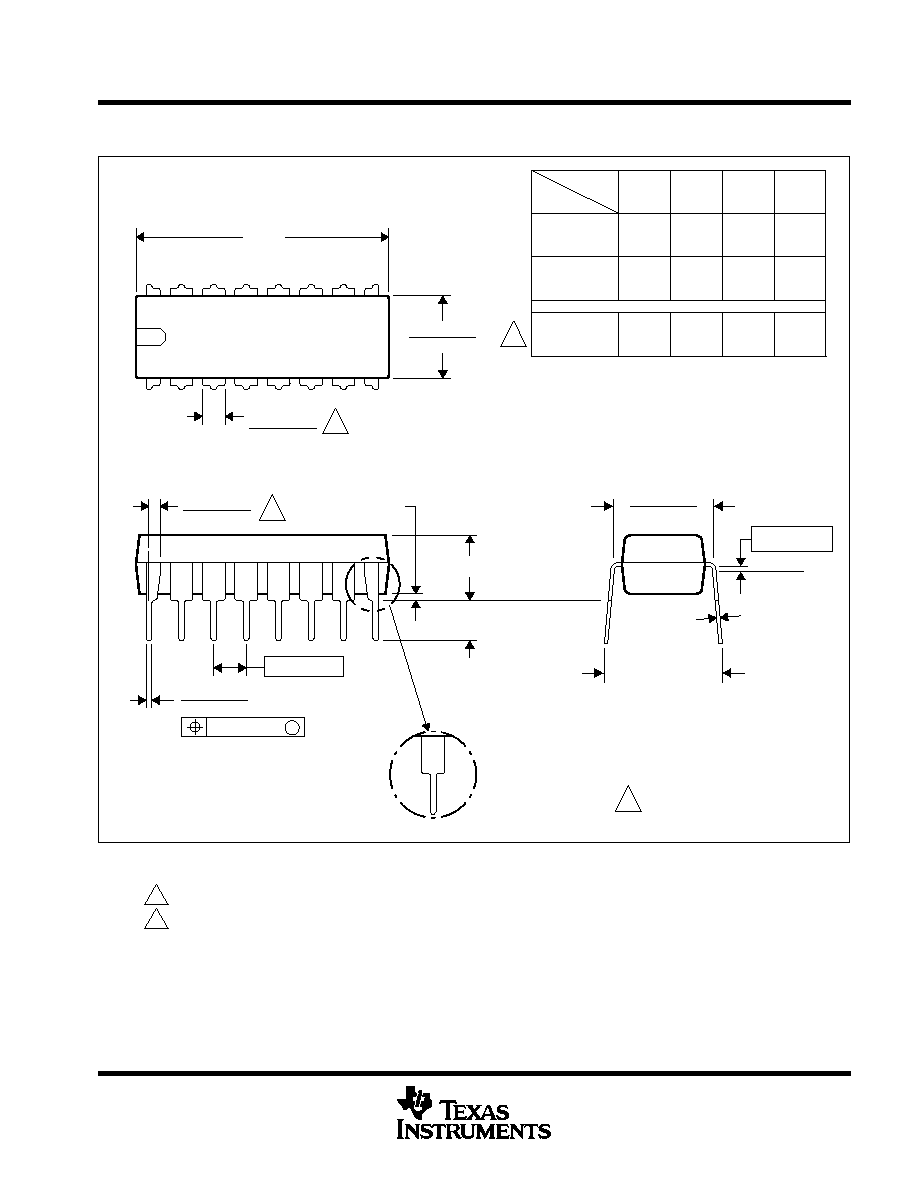
N (R-PDIP-T**)
PLASTIC DUAL-IN-LINE PACKAGE
BB
AC
AD
0.325 (8,26)
0.300 (7,62)
0.010 (0,25) NOM
Gauge Plane
0.015 (0,38)
0.430 (10,92) MAX
20
1.060
(26,92)
0.940
(23,88)
18
0.920
0.850
14
0.775
0.745
(19,69)
(18,92)
16
0.775
(19,69)
(18,92)
0.745
A MIN
DIM
A MAX
PINS **
(23,37)
(21,59)
Seating Plane
14/18 PIN ONLY
20 pin vendor option
4040049/E 12/2002
9
8
0.070 (1,78)
A
0.045 (1,14)
0.020 (0,51) MIN
16
1
0.015 (0,38)
0.021 (0,53)
0.200 (5,08) MAX
0.125 (3,18) MIN
0.240 (6,10)
0.260 (6,60)
M
0.010 (0,25)
0.100 (2,54)
16 PINS SHOWN
MS-100
VARIATION
AA
C
D
D
D
0.030 (0,76)
0.045 (1,14)
NOTES: A. All linear dimensions are in inches (millimeters).
B. This drawing is subject to change without notice.
C. Falls within JEDEC MS-001, except 18 and 20 pin minimum body lrngth (Dim A).
D. The 20 pin end lead shoulder width is a vendor option, either half or full width.
MECHANICAL DATA
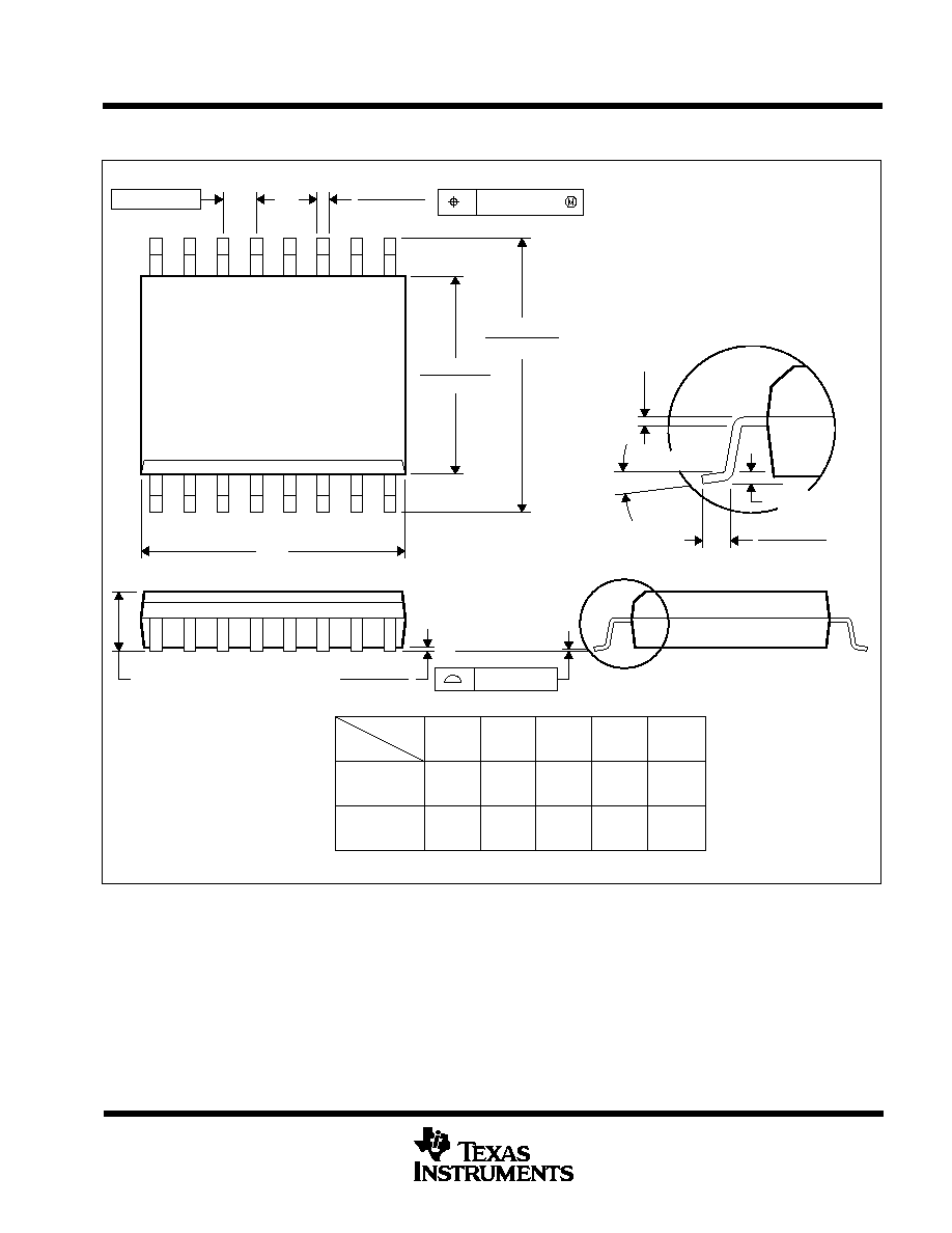
MSOI003E ≠ JANUARY 1995 ≠ REVISED SEPTEMBER 2001
1
POST OFFICE BOX 655303
∑
DALLAS, TEXAS 75265
DW (R-PDSO-G**)
PLASTIC SMALL-OUTLINE PACKAGE
16 PINS SHOWN
0.419 (10,65)
0.400 (10,15)
0.291 (7,39)
0.299 (7,59)
16
0.400
(10,16)
A MIN
A MAX
(10,41)
0.410
0.462
(11,73)
(11,51)
0.453
18
0.610
(15,49)
(15,24)
0.600
24
DIM
PINS **
4040000/E 08/01
0.104 (2,65) MAX
0.004 (0,10)
0.012 (0,30)
Seating Plane
0
∞
≠ 8
∞
0.016 (0,40)
0.050 (1,27)
16
0.050 (1,27)
1
A
8
9
0.014 (0,35)
0.020 (0,51)
0.010 (0,25) NOM
Gage Plane
0.010 (0,25)
28
0.710
(18,03)
0.700
(17,78)
(12,70)
(12,95)
0.500
20
0.510
0.010 (0,25)
0.004 (0,10)
NOTES: A. All linear dimensions are in inches (millimeters).
B. This drawing is subject to change without notice.
C. Body dimensions do not include mold flash or protrusion not to exceed 0.006 (0,15).
D. Falls within JEDEC MS-013

IMPORTANT NOTICE
Texas Instruments Incorporated and its subsidiaries (TI) reserve the right to make corrections, modifications,
enhancements, improvements, and other changes to its products and services at any time and to discontinue
any product or service without notice. Customers should obtain the latest relevant information before placing
orders and should verify that such information is current and complete. All products are sold subject to TI's terms
and conditions of sale supplied at the time of order acknowledgment.
TI warrants performance of its hardware products to the specifications applicable at the time of sale in
accordance with TI's standard warranty. Testing and other quality control techniques are used to the extent TI
deems necessary to support this warranty. Except where mandated by government requirements, testing of all
parameters of each product is not necessarily performed.
TI assumes no liability for applications assistance or customer product design. Customers are responsible for
their products and applications using TI components. To minimize the risks associated with customer products
and applications, customers should provide adequate design and operating safeguards.
TI does not warrant or represent that any license, either express or implied, is granted under any TI patent right,
copyright, mask work right, or other TI intellectual property right relating to any combination, machine, or process
in which TI products or services are used. Information published by TI regarding third≠party products or services
does not constitute a license from TI to use such products or services or a warranty or endorsement thereof.
Use of such information may require a license from a third party under the patents or other intellectual property
of the third party, or a license from TI under the patents or other intellectual property of TI.
Reproduction of information in TI data books or data sheets is permissible only if reproduction is without
alteration and is accompanied by all associated warranties, conditions, limitations, and notices. Reproduction
of this information with alteration is an unfair and deceptive business practice. TI is not responsible or liable for
such altered documentation.
Resale of TI products or services with statements different from or beyond the parameters stated by TI for that
product or service voids all express and any implied warranties for the associated TI product or service and
is an unfair and deceptive business practice. TI is not responsible or liable for any such statements.
Mailing Address:
Texas Instruments
Post Office Box 655303
Dallas, Texas 75265
Copyright
2003, Texas Instruments Incorporated