 | ÐлекÑÑоннÑй компоненÑ: ADS8342 | СкаÑаÑÑ:  PDF PDF  ZIP ZIP |
Äîêóìåíòàöèÿ è îïèñàíèÿ www.docs.chipfind.ru
SBAS277 MAY 2003
16 Bit, 250kSPS, 4 Channel, Parallel Output
ANALOG TO DIGITAL CONVERTER
ADS8342
FEATURES
D
True Bipolar Input
D
Input Signal Range:
±
2.5V
D
4-Channel Input Multiplexer
D
Up to 250kSPS Sampling Rate
D
Selectable 8-Bit or 16-Bit Parallel Interface
D
16-Bit Ensured No Missing Codes
D
Offset: 1mV
max
D
Low Power: 200mW
D
TQFP-48 Package
D
Operating Temperature Range: 40
°
C to +85
°
C
APPLICATIONS
D
Data Acquisition
D
Test and Measurement
D
Industrial Process Control
D
Medical Instruments
D
Laboratory Equipment
DESCRIPTION
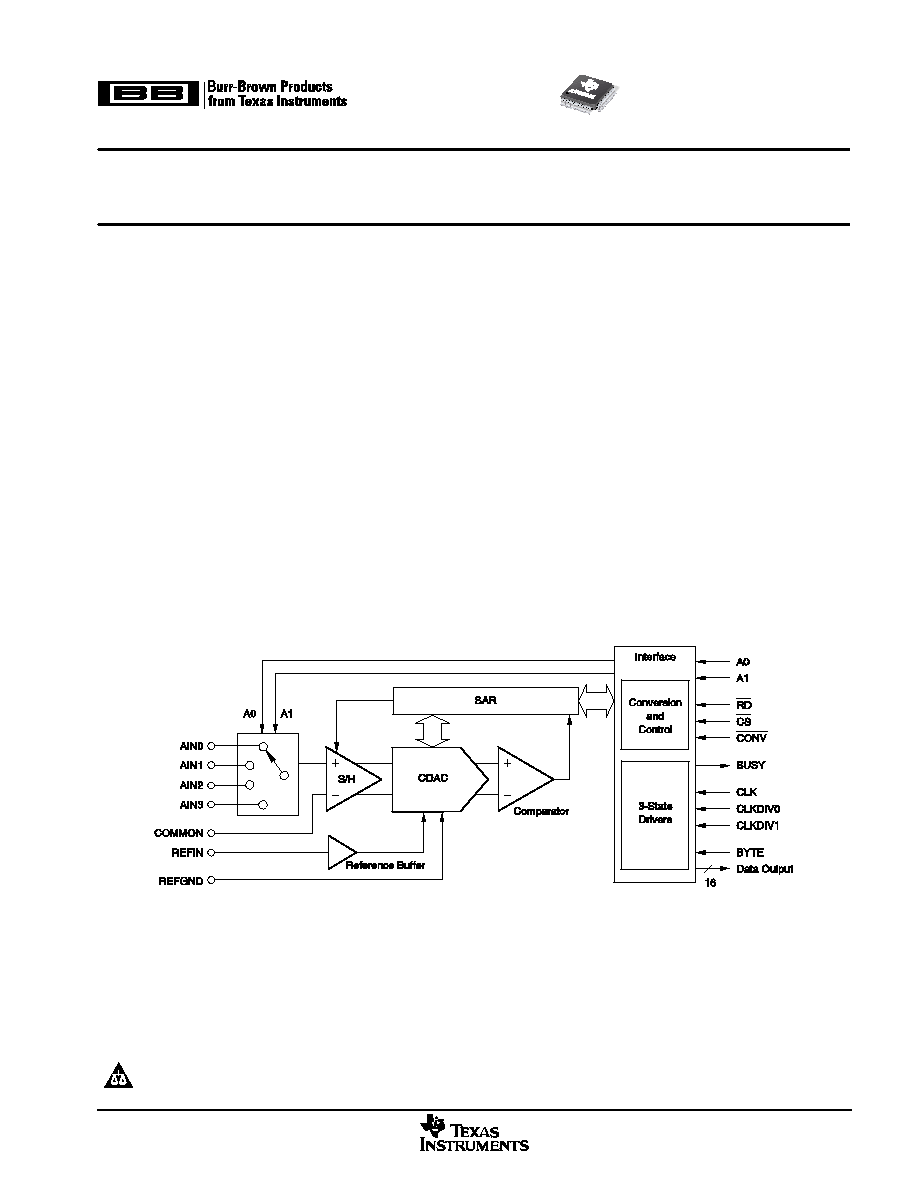
The ADS8342 is a 4-channel, 16-bit analog-to-digital
converter (ADC). It contains a 16-bit succesive
approximation register (SAR), a capacitor-based ADC with
an inherent sample-and-hold circuit, an interface for
microprocessor use, and parallel 3-state output drivers. The
ADS8342 is specified at a 250kHz sampling rate while
dissipating only 200mW of power using a
±
5V power supply.
The ADS8342 is available in a TQFP-48 package and is
ensured over the 40
°
C to +85
°
C temperature range.
www.ti.com
Copyright
2003, Texas Instruments Incorporated
Please be aware that an important notice concerning availability, standard warranty, and use in critical applications of Texas Instruments
semiconductor products and disclaimers thereto appears at the end of this data sheet.
PRODUCTION DATA information is current as of publication date. Products
conform to specifications per the terms of Texas Instruments standard warranty.
Production processing does not necessarily include testing of all parameters.
ADS8342
SBAS277 MAY 2003
www.ti.com
2
This integrated circuit can be damaged by ESD. Texas Instruments recommends that all integrated
circuits be handled with appropriate precautions. Failure to observe proper handling and installation
procedures can cause damage.
ESD damage can range from subtle performance degradation to complete device failure. Precision integrated circuits
may be more susceptible to damage because very small parametric changes could cause the device not to meet
its published specifications.
ORDERING INFORMATION
PRODUCT
MAXIMUM
INTEGRAL
LINEARITY
ERROR
(LSB)
NO
MISSING
CODES
(Bits)
PACKAGE
LEAD
PACKAGE
DESIGNATOR(1)
SPECIFIED
TEMPERATURE
RANGE
ORDERING
NUMBER
TRANSPORT
MEDIA,
QUANTITY
ADS8342
±
6
15
TQFP 48
PFB
40
°
C t
85
°
C
ADS8342IPFBT
Tape and Reel,
250
ADS8342
±
6
15
TQFP-48
PFB
40
°
C to +85
°
C
ADS8342IPFBR
Tape and Reel,
2000
ADS8342
±
4
16
TQFP 48
PFB
40
°
C t
85
°
C
ADS8342IBPFBT
Tape and Reel,
250
ADS8342
±
4
16
TQFP-48
PFB
40
°
C to +85
°
C
ADS8342IBPFBR
Tape and Reel,
2000
(1) For the most current specification and package information, refer to our web site at www.ti.com.
ABSOLUTE MAXIMUM RATINGS
over operating free-air temperature range unless otherwise noted(1)
ADS8342I
UNIT
Supply voltage, +AVDD to AGND and +DVDD to DGND
0.3 to 6
V
Supply voltage, AVDD to AGND and DVDD to DGND
6 to 0.3
V
Supply voltage, BVDD to BGND
0.3 to 6
V
Analog input voltage to AGND
AVDD 0.3 to +AVDD + 0.3
V
Reference voltage, REFIN to AGND
0.3 to +AVDD + 0.3
V
Common voltage to AGND
0.3 to +0.3
V
Digital input voltage to BGND
BGND 0.3 to BVDD + 0.3
V
Ground voltage differences, AGND to REFGND or BGND or DGND
0.3 to 0.3
V
Voltage differences, BVDD or +DVDD to AGND
0.3 to 6
V
Voltage differences, +DVDD to +AVDD and DVDD to AVDD
0.3 to 0.3
V
Voltage differences, BVDD to DVDD
(+DVDD) to 0.3
V
Input current to any pin except supply
20 to 20
mA
Power dissipation
see Package Dissipation Ratings table
Operating virtual junction temperature range, TJ
40 to +150
°
C
Operating free-air temperature range, TA
40 to +85
°
C
Storage temperature range, TSTG
65 to +150
°
C
Lead temperature 1.6mm (1/16 inch) from case for 10 seconds
+300
°
C
(1) Stresses above these ratings may cause permanent damage. Exposure to absolute maximum conditions for extended periods may degrade
device reliability. These are stress ratings only, and functional operation of the device at these or any other conditions beyond those specified is
not implied.
ADS8342
SBAS277 MAY 2003
www.ti.com
3
PACKAGE DISSIPATION RATINGS
BOARD
PACKAGE
R
JC
(
°
C/W)
R
JA
(
°
C/W)
DERATING FACTOR
ABOVE TA
+25
°
C
(mW/
°
C)
TA
+25
°
C
POWER RATING
(mW)
TA
+70
°
C
POWER RATING
(mW)
TA = +85
°
C
POWER RATING
(mW)
Low K
PFB
19.6
97.5
10.256
1282
820
666
High K
PFB
19.6
63.7
15.698
1962
1255
1020
(1) The JEDEC Low K(1s) board design used to derive this data was a 3 inch x 3 inch, 2-layer board with 2-ounce copper traces on top of the board.
(2) The JEDEC High K(2s2p) board design used to derive this data was a 3 inch x 3 inch, multilayer board with 1-ounce internal power and ground
planes and 2-ounce copper traces on the top and bottom of the board.
RECOMMENDED OPERATING CONDITIONS
MIN
NOM
MAX
UNIT
Supply voltage, +AVDD to AGND
4.75
5
5.25
V
Supply voltage, AVDD to AGND
5.25
5
4.75
V
Supply voltage BV
to BGND
Low-voltage levels
2.7
3.6
V
Supply voltage, BVDD to BGND
5V logic levels
4.5
+DVDD
V
Supply voltage, +DVDD to DGND
4.75
5
5.25
V
Supply voltage, DVDD to DGND
5.25
5
4.75
V
Reference input voltage
2.0
2.5
2.55
V
Analog input voltage
REFIN
+REFIN
V
Common voltage
0.3
0
+0.3
V
Ground differences, AGND to REFGND or BGND or DGND
0.01
0
0.01
V
Voltage differences, +DVDD to +AVDD and DVDD to AVDD
0.01
0
0.01
V
EQUIVALENT INPUT CIRCUIT
ADS8342
SBAS277 MAY 2003
www.ti.com
4
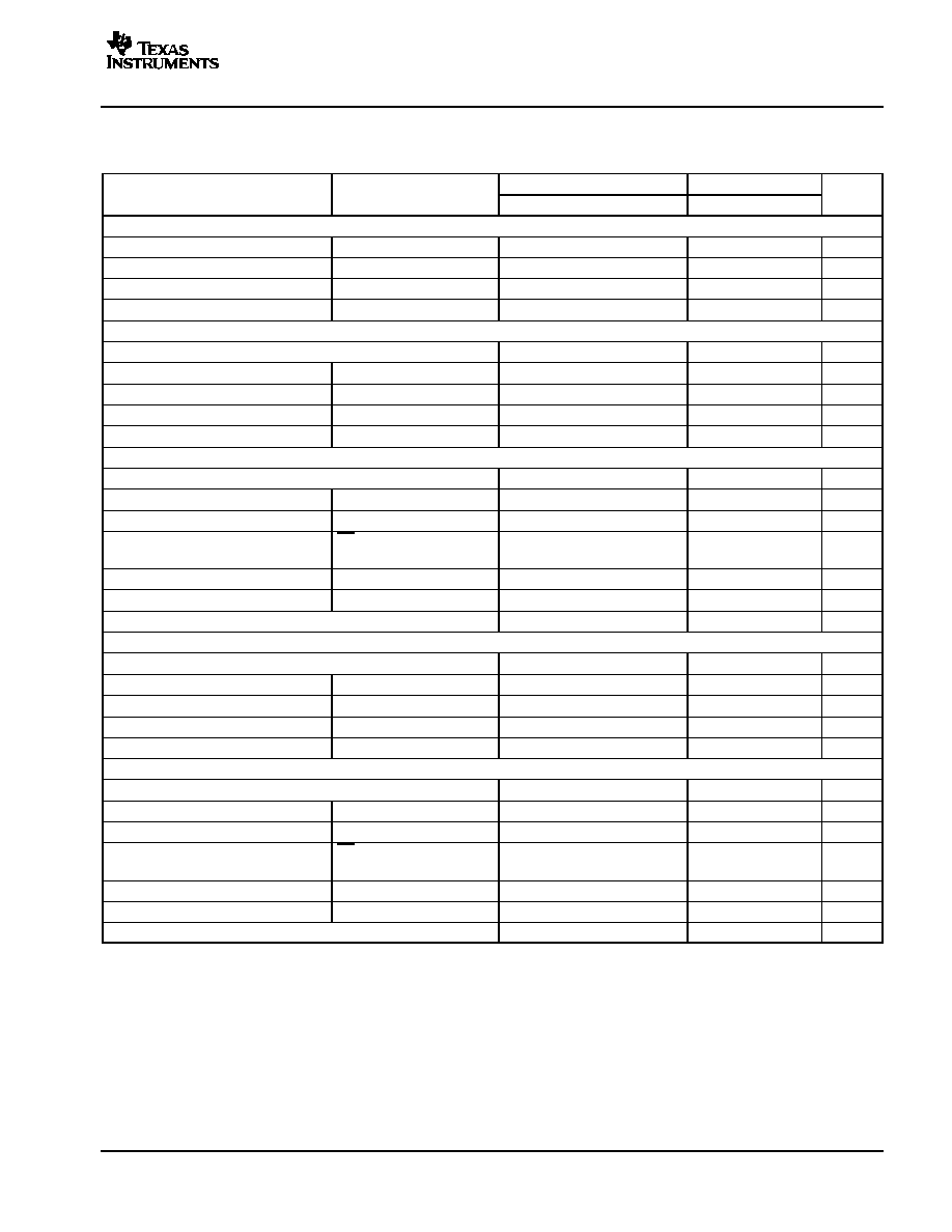
ELECTRICAL CHARACTERISTICS
Over recommended operating free-air temperature range at 40
°
C to +85
°
C,
±
AVDD =
±
DVDD =
±
5V, BVDD = +5V, VREF = +2.5V, fCLK = 5MHz, and
fSAMPLE = 250kSPS, unless otherwise noted.
PARAMETER
TEST CONDITIONS
ADS8342I
ADS8342IB
UNIT
PARAMETER
TEST CONDITIONS
MIN
TYP(1)
MAX
MIN
TYP(1)
MAX
UNIT
Analog Input
Full-scale range (FSR)
AIN to Common
VREF
+VREF
:
:
V
Input MUX on-resistance
Common = AGND
500
:
Input capacitance
Common = AGND
20
:
pF
Input leakage current
Common = AGND
±
0.3
:
µ
A
Full power bandwidth
FS sinewave, 3dB
16
:
MHz
Voltage Accuracy
Resolution
16
:
Bits
No missing code
(NMC)
15
16
Bits
Integral linearity error (INL)
6
±
3
+6
4
±
2
+4
LSB
Differential nonlinearity (DNL)
2
±
1
+2
1
±
0.6
+1.5
LSB
Bipolar zero (offset) error (VOS)
AIN = Common = 0V
2
+2
1
+1
mV
Bipolar zero (offset) error drift (TCVOS)
AIN = Common = 0V
1
:
ppm/
°
C
Bipolar zero (offset) error match
AIN = Common = 0V
0.150
1
:
:
mV
Positive gain error (PGERR)
AIN = VREF, Common = 0V
0.25
+0.25
:
:
% FSR
Positive gain error drift (TCPGERR)
AIN = VREF, Common = 0V
1.5
:
ppm/
°
C
Positive gain error match
AIN = VREF, Common = 0V
0.003
0.01
:
:
% FSR
Negative gain error (NGERR)
AIN = VREF, Common = 0V
0.25
+0.25
:
:
% FSR
Negative gain error drift (TCNGERR)
AIN = VREF, Common = 0V
1.5
:
ppm/
°
C
Negative gain error match
AIN = VREF, Common = 0V
0.003
0.01
:
:
% FSR
Sampling Dynamics
Conversion time (tCONV)
500kHz
fCLK
5MHz
3.4
34
:
:
µ
s
Acquisition time (tACQ)
fCLK = 5MHz
0.6
:
:
µ
s
Throughput rate
250
:
kHz
Multiplexer settling time
150
:
ns
Aperture delay
8
:
ns
Aperture jitter
50
:
ps
AC Accuracy
Total haromonic distortion (THD)
VIN =
±
2.5Vpp at 10kHz
89
:
dB
Spurious-free dynamic range (SFDR)
VIN =
±
2.5Vpp at 10kHz
92
:
dB
Signal-to-noise ratio (SNR)
VIN =
±
2.5Vpp at 10kHz
86
:
dB
Signal-to-noise + distortion (SINAD)
VIN =
±
2.5Vpp at 10kHz
84.6
:
dB
Channel-to-channel isolation(2)
VIN =
±
2.5Vpp at 50kHz
95
:
dB
Effective number of bits (ENOB)
14
:
Bits
:
Indicates the same specifications as the ADS8342I.
(1) All typical values are at TA = +25
°
C.
(2) Ensured by design.
(3) Applies for 5.0V nominal supply: BVDD (min) = 4.5V and BVDD (max) = 5.5V.
(4) Applies for 3.0V nominal supply: BVDD (min) = 2.7V and BVDD (max) = 3.6V.
ADS8342
SBAS277 MAY 2003
www.ti.com
5
ELECTRICAL CHARACTERISTICS (continued)
Over recommended operating free-air temperature range at 40
°
C to +85
°
C,
±
AVDD =
±
DVDD =
±
5V, BVDD = +5V, VREF = +2.5V, fCLK = 5MHz, and
fSAMPLE = 250kSPS, unless otherwise noted.
PARAMETER
UNIT
ADS8342IB
ADS8342I
TEST CONDITIONS
PARAMETER
UNIT
MAX
TYP(1)
MIN
MAX
TYP(1)
MIN
TEST CONDITIONS
Voltage Reference Input
Reference voltage
2.0
2.5
2.55
:
:
:
V
Reference input resistance
100
:
M
Reference input capacitance
5
:
pF
Reference input current
25
:
nA
5V Digital Inputs(3)
Logic family
CMOS
High-level input voltage (VIH)
0.7
×
BVDD
BVDD + 0.3
V
Low-level input voltage (VIL)
0.3
0.3
×
BVDD
V
Input leakage current (IIN)
VI = BVDD or GND
±
50
nA
Input capacitance (CI)
5
pF
5V Digital Outputs(3)
Logic family
CMOS
High-level output voltage (VOH)
IOH = 100
µ
A
4.4
V
Low-level output voltage (VOL)
IOL = +100
µ
A
0.5
V
High-impeadance-state output current
(IOZ)
CS = BVDD, VO = BVDD or
GND
±
50
nA
Output capacitance (CO)
5
pF
Load capacitance (CL)
20
pF
Data format
Binary Two's Complement
3V Digital Inputs(4)
Logic family
LVCMOS
High-level input voltage (VIH)
BVDD = 3.6V
2
BVDD + 0.3
V
Low-level input voltage (VIL)
BVDD = 2.7V
0.3
0.8
V
Input leakage current (IIN)
VI = BVDD or GND
±
50
nA
Input capacitance (CI)
5
pF
3V Digital Outputs(4)
Logic family
LVCMOS
High-level output voltage (VOH)
BVDD = 2.7V, IOH = 100
µ
A
BVDD 0.3
V
Low-level output voltage (VOL)
BVDD = 2.7V, IOL = +100
µ
A
0.2
V
High-impeadance-state output current
(IOZ)
CS = BVDD, VO = BVDD or
GND
±
50
nA
Output capacitance (CO)
5
pF
Load capacitance (CL)
20
pF
Data format
Binary Two's Complement
:
Indicates the same specifications as the ADS8342I.
(1) All typical values are at TA = +25
°
C.
(2) Ensured by design.
(3) Applies for 5.0V nominal supply: BVDD (min) = 4.5V and BVDD (max) = 5.5V.
(4) Applies for 3.0V nominal supply: BVDD (min) = 2.7V and BVDD (max) = 3.6V.