1
Data sheet acquired from Harris Semiconductor
SCHS168D
Features
∑ Typical Propagation Delay (A to B, B to A) of 7ns at
V
CC
= 5V, C
L
= 15pF, T
A
= 25
o
C
∑ Three-State Outputs
∑ Buffered Inputs
∑ Fanout (Over Temperature Range)
- Standard Outputs . . . . . . . . . . . . . . . 10 LSTTL Loads
- Bus Driver Outputs . . . . . . . . . . . . . 15 LSTTL Loads
∑ Wide Operating Temperature Range . . . -55
o
C to 125
o
C
∑ Balanced Propagation Delay and Transition Times
∑ Significant Power Reduction Compared to LSTTL
Logic ICs
∑ HC Types
- 2V to 6V Operation
- High Noise Immunity: N
IL
= 30%, N
IH
= 30% of V
CC
at V
CC
= 5V
∑ HCT Types
- 4.5V to 5.5V Operation
- Direct LSTTL Input Logic Compatibility,
V
IL
= 0.8V (Max), V
IH
= 2V (Min)
- CMOS Input Compatibility, I
l
1
µ
A at V
OL
, V
OH
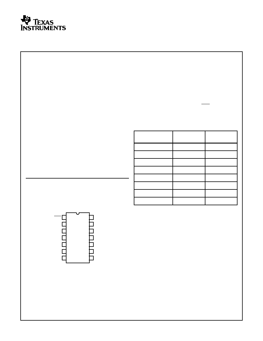
Pinout
CD54HC243, CD54HCT243
(CERDIP)
CD74HC243, CD74HCT243
(PDIP, SOIC)
TOP VIEW
Description
The 'HC243 and 'HCT243 silicon-gate CMOS three-state
bidirectional noninverting buffers are intended for two-way
asynchronous communication between data buses. They
have high-drive-current outputs that enable high-speed oper-
ation when driving large bus capacitances. These circuits
possess the low power dissipation of CMOS circuits and
have speeds comparable to low-power Schottky TTL circuits.
They can drive 15 LSTTL loads.
The states of the output-enable (OEB, OEA) inputs
determine both the direction of flow (A to B, B to A), and the
three-state mode.
OEB
NC
A0
A1
A2
A3
GND
V
CC
OEA
NC
B0
B1
B2
B3
1
2
3
4
5
6
7
14
13
12
11
10
9
8
Ordering Information
PART NUMBER
TEMP. RANGE
(
o
C)
PACKAGE
CD54HC243F3A
-55 to 125
14 Ld CERDIP
CD54HCT243F3A
-55 to 125
14 Ld CERDIP
CD74HC243E
-55 to 125
14 Ld PDIP
CD74HC243M
-55 to 125
14 Ld SOIC
CD74HC243MT
-55 to 125
14 Ld SOIC
CD74HC243M96
-55 to 125
14 Ld SOIC
CD74HCT243E
-55 to 125
14 Ld PDIP
CD74HCT243M
-55 to 125
14 Ld SOIC
NOTE: When ordering, use the entire part number. The suffix 96
denotes tape and reel. The suffix T denotes a small-quantity reel of
250.
November 1997 - Revised October 2003
CAUTION: These devices are sensitive to electrostatic discharge. Users should follow proper IC Handling Procedures.
Copyright
©
2003, Texas Instruments Incorporated
CD54HC243, CD74HC243,
CD54HCT243, CD74HCT243
High-Speed CMOS Logic
Quad-Bus Transceiver with Three-State Outputs
[ /Title
(CD74
HCT24
2,
CD74
HC243
,
CD74
HCT24
3)
/Sub-
ject
(High
Speed
CMOS
Logic
Quad-
2
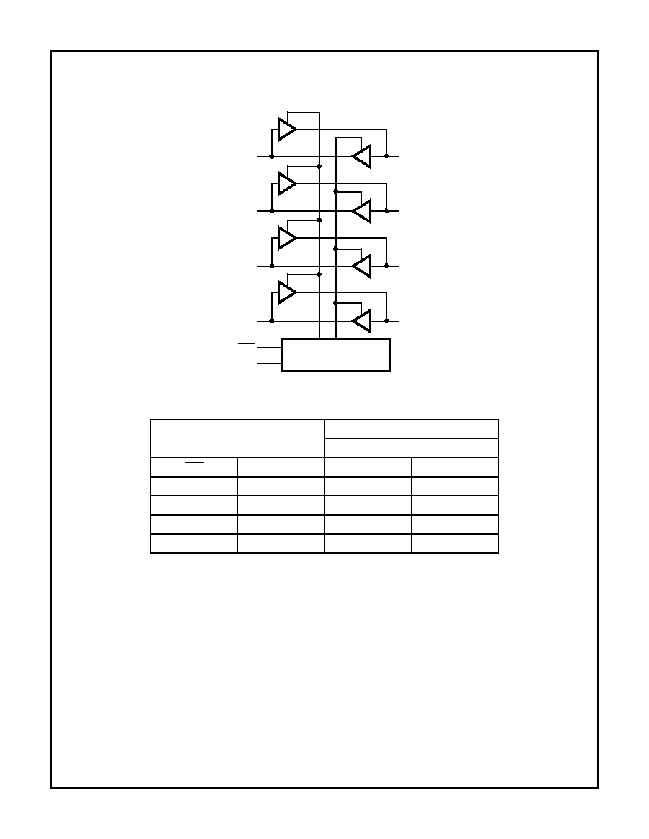
Functional Diagram
`HC243, `HCT243
TRUTH TABLE
CONTROL INPUTS
HC, HCT243 SERIES
DATA PORT STATUS
OEB
OEA
An
Bn
H
H
O
I
L
H
Z
Z
H
L
Z
Z
L
L
I
O
H= High Voltage Level
L= Low Voltage Level
I= Input
O= Output (Same Level as Input)
Z= High Impedance
To prevent excess currents in the High Z modes all I/O terminals should be terminated with 10k
to 1M
resistors.
DIRECTION
SELECT LOGIC
A0
A1
A2
A3
OEB
OEA
3
4
5
6
1
13
11
10
9
8
B0
B1
B2
B3
CD54HC243, CD74HC243, CD54HCT243, CD74HCT243
3
Absolute Maximum Ratings
Thermal Information
DC Supply Voltage, V
CC
. . . . . . . . . . . . . . . . . . . . . . . . -0.5V to 7V
DC Input Diode Current, I
IK
For V
I
< -0.5V or V
I
> V
CC
+ 0.5V
. . . . . . . . . . . . . . . . . . . . . .±
20mA
DC Output Diode Current, I
OK
For V
O
< -0.5V or V
O
> V
CC
+ 0.5V
. . . . . . . . . . . . . . . . . . . .±
20mA
DC Drain Current, per Output, I
O
For -0.5V < V
O
< V
CC
+ 0.5V
. . . . . . . . . . . . . . . . . . . . . . . . . .±
35mA
DC Output Source or Sink Current per Output Pin, I
O
For V
O
> -0.5V or V
O
< V
CC
+ 0.5V
. . . . . . . . . . . . . . . . . . . .±
25mA
DC V
CC
or Ground Current, I
CC
. . . . . . . . . . . . . . . . . . . . . . . . .±
70mA
Operating Conditions
Temperature Range (T
A
) . . . . . . . . . . . . . . . . . . . . . -55
o
C to 125
o
C
Supply Voltage Range, V
CC
HC Types . . . . . . . . . . . . . . . . . . . . . . . . . . . . . . . . . . . . .2V to 6V
HCT Types . . . . . . . . . . . . . . . . . . . . . . . . . . . . . . . . .4.5V to 5.5V
DC Input or Output Voltage, V
I
, V
O
. . . . . . . . . . . . . . . . . 0V to V
CC
Input Rise and Fall Time
2V . . . . . . . . . . . . . . . . . . . . . . . . . . . . . . . . . . . . . . 1000ns (Max)
4.5V. . . . . . . . . . . . . . . . . . . . . . . . . . . . . . . . . . . . . . 500ns (Max)
6V . . . . . . . . . . . . . . . . . . . . . . . . . . . . . . . . . . . . . . . 400ns (Max)
Thermal Resistance (Typical, Note 1)
JA
(
o
C/W)
E (PDIP) Package . . . . . . . . . . . . . . . . . . . . . . . . . . . . . . 80
M (SOIC) Package. . . . . . . . . . . . . . . . . . . . . . . . . . . . . . 86
Maximum Junction Temperature . . . . . . . . . . . . . . . . . . . . . . . 150
o
C
Maximum Storage Temperature Range . . . . . . . . . .-65
o
C to 150
o
C
Maximum Lead Temperature (Soldering 10s) . . . . . . . . . . . . . 300
o
C
(SOIC - Lead Tips Only)
CAUTION: Stresses above those listed in "Absolute Maximum Ratings" may cause permanent damage to the device. This is a stress only rating and operation
of the device at these or any other conditions above those indicated in the operational sections of this specification is not implied.
NOTE:
1. The package thermal impedance is calculated in accordance with JESD 51-7.
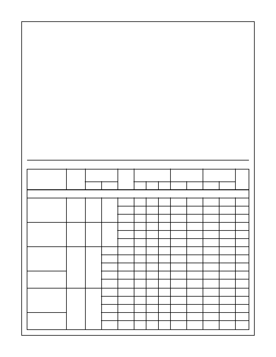
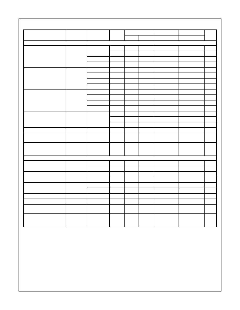
DC Electrical Specifications
PARAMETER
SYMBOL
TEST
CONDITIONS
V
CC
(V)
25
o
C
-40
o
C TO 85
o
C
-55
o
C TO 125
o
C
UNITS
V
I
(V)
I
O
(mA)
MIN
TYP
MAX
MIN
MAX
MIN
MAX
HC TYPES
High Level Input
Voltage
V
IH
-
-
2
1.5
-
-
1.5
-
1.5
-
V
4.5
3.15
-
-
3.15
-
3.15
-
V
6
4.2
-
-
4.2
-
4.2
-
V
Low Level Input
Voltage
V
IL
-
-
2
-
-
0.5
-
0.5
-
0.5
V
4.5
-
-
1.35
-
1.35
-
1.35
V
6
-
-
1.8
-
1.8
-
1.8
V
High Level Output
Voltage
CMOS Loads
V
OH
V
IH
or
V
IL
-0.02
2
1.9
-
-
1.9
-
1.9
-
V
-0.02
4.5
4.4
-
-
4.4
-
4.4
-
V
-0.02
6
5.9
-
-
5.9
-
5.9
-
V
High Level Output
Voltage
TTL Loads
-6
4.5
3.98
-
-
3.84
-
3.7
-
V
-7.8
6
5.48
-
-
5.34
-
5.2
-
V
Low Level Output
Voltage
CMOS Loads
V
OL
V
IH
or
V
IL
0.02
2
-
-
0.1
-
0.1
-
0.1
V
0.02
4.5
-
-
0.1
-
0.1
-
0.1
V
0.02
6
-
-
0.1
-
0.1
-
0.1
V
Low Level Output
Voltage
TTL Loads
6
4.5
-
-
0.26
-
0.33
-
0.4
V
7.8
6
-
-
0.26
-
0.33
-
0.4
V
CD54HC243, CD74HC243, CD54HCT243, CD74HCT243
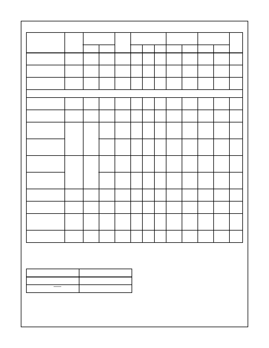
4
Input Leakage
Current
I
I
V
CC
or
GND
-
6
-
-
±
0.1
-
±
1
-
±
1
µ
A
Quiescent Device
Current
I
CC
V
CC
or
GND
0
6
-
-
8
-
80
-
160
µ
A
Three-State Leakage
Current
I
OZ
V
IL
or
V
IH
-
6
-
-
±
0.5
-
±
0.5
-
±
10
µ
A
HCT TYPES
High Level Input
Voltage
V
IH
-
-
4.5 to
5.5
2
-
-
2
-
2
-
V
Low Level Input
Voltage
V
IL
-
-
4.5 to
5.5
-
-
0.8
-
0.8
-
0.8
V
High Level Output
Voltage
CMOS Loads
V
OH
V
IH
or
V
IL
-0.02
4.5
4.4
-
-
4.4
-
4.4
-
V
High Level Output
Voltage
TTL Loads
-6
4.5
3.98
-
-
3.84
-
3.7
-
V
Low Level Output
Voltage
CMOS Loads
V
OL
V
IH
or
V
IL
0.02
4.5
-
-
0.1
-
0.1
-
0.1
V
Low Level Output
Voltage
TTL Loads
6
4.5
-
-
0.26
-
0.33
-
0.4
V
Input Leakage
Current
I
I
V
CC
to
GND
-
5.5
-
-
±
0.1
-
±
1
-
±
1
µ
A
Quiescent Device
Current
I
CC
V
CC
or
GND
0
5.5
-
-
8
-
80
-
160
µ
A
Additional Quiescent
Device Current Per
Input Pin: 1 Unit Load
I
CC
(Note 2)
V
CC
-2.1
-
4.5 to
5.5
-
100
360
-
450
-
490
µ
A
Three-State Leakage
Current
I
OZ
V
IL
or
V
IH
-
5.5
-
-
±
0.5
-
±
5.0
-
±
10
µ
A
NOTE:
2. For dual-supply systems theoretical worst case (V
I
= 2.4V, V
CC
= 5.5V) specification is 1.8mA.
DC Electrical Specifications
(Continued)
PARAMETER
SYMBOL
TEST
CONDITIONS
V
CC
(V)
25
o
C
-40
o
C TO 85
o
C
-55
o
C TO 125
o
C
UNITS
V
I
(V)
I
O
(mA)
MIN
TYP
MAX
MIN
MAX
MIN
MAX
HCT Input Loading Table
INPUT
UNIT LOADS
An, Bn
1.1
OEA, OEB
0.6
NOTE: Unit Load is
I
CC
limit specified in DC Electrical
Specifications table, e.g., 360
µ
A max at 25
o
C.
CD54HC243, CD74HC243, CD54HCT243, CD74HCT243
5
Switching Specifications
Input t
r
, t
f
= 6ns
PARAMETER
SYMBOL
TEST
CONDITIONS
V
CC
(V)
25
o
C
-40
o
C TO 85
o
C
-55
o
C TO 125
o
C
UNITS
TYP
MAX
MAX
MAX
HC TYPES
Propagation Delay Data
to Outputs
t
PLH
, t
PHL
C
L
= 50pF
2
-
90
115
135
ns
4.5
-
18
23
27
ns
C
L
= 15pF
5
7
-
-
-
ns
CL = 50pF
6
-
15
20
23
ns
Output High-Z, to High Level
to Low Level
t
PZL,
t
PZH
C
L
= 50pF
2
-
150
190
225
ns
CL = 50pF
4.5
-
30
38
45
ns
CL = 15pF
5
12
-
-
-
ns
CL = 50pF
6
-
26
33
38
ns
Output High Level,
Output Low Level to High-Z
t
PHZ,
t
PLZ
C
L
= 50pF
2
-
150
190
225
ns
CL = 50pF
4.5
-
30
38
45
ns
CL = 15pF
5
12
-
-
-
ns
CL = 50pF
6
-
26
33
38
ns
Output Transition Times
t
TLH
, t
THL
C
L
= 50pF
2
-
60
75
90
ns
4.5
-
12
15
18
ns
6
-
10
13
15
ns
Input Capacitance
C
I
-
-
-
10
10
10
pF
Three-State Output
Capacitance
C
O
-
-
-
20
20
20
pF
Power Dissipation
Capacitance
(Notes 3, 4)
C
PD
-
5
80
-
-
-
pF
HCT TYPES
Propagation Delay Data to
Outputs
t
PLH
, t
PHL
C
L
= 50pF
4.5
-
22
28
33
ns
C
L
= 15pF
5
9
-
-
-
ns
Output High-Z to High Level
to Low Level
t
PZH
, t
PZL
C
L
= 50pF
4.5
-
34
43
51
ns
C
L
= 15pF
5
14
-
-
-
ns
Output High Level,
Output Low Level to High-Z
t
PHZ
, t
PLZ
C
L
= 50pF
4.5
-
35
44
53
ns
C
L
= 15pF
5
14
-
-
-
ns
Output Transition Times
t
TLH
, t
THL
C
L
= 50pF
4.5
-
12
15
18
ns
Input Capacitance
C
I
-
-
-
10
10
10
pF
Three-State Output
Capacitance
C
O
-
-
-
20
20
20
pF
Power Dissipation
Capacitance
(Notes 3, 4)
C
PD
-
5
91
-
-
-
pF
NOTES:
3. C
PD
is used to determine the dynamic power consumption, per channel.
4. P
D
= V
CC
2
f
i
(C
PD
+ C
L
) where f
i
= Input Frequency, f
O
= Output Frequency, C
L
= Output Load Capacitance, V
CC
= Supply Voltage.
CD54HC243, CD74HC243, CD54HCT243, CD74HCT243
6
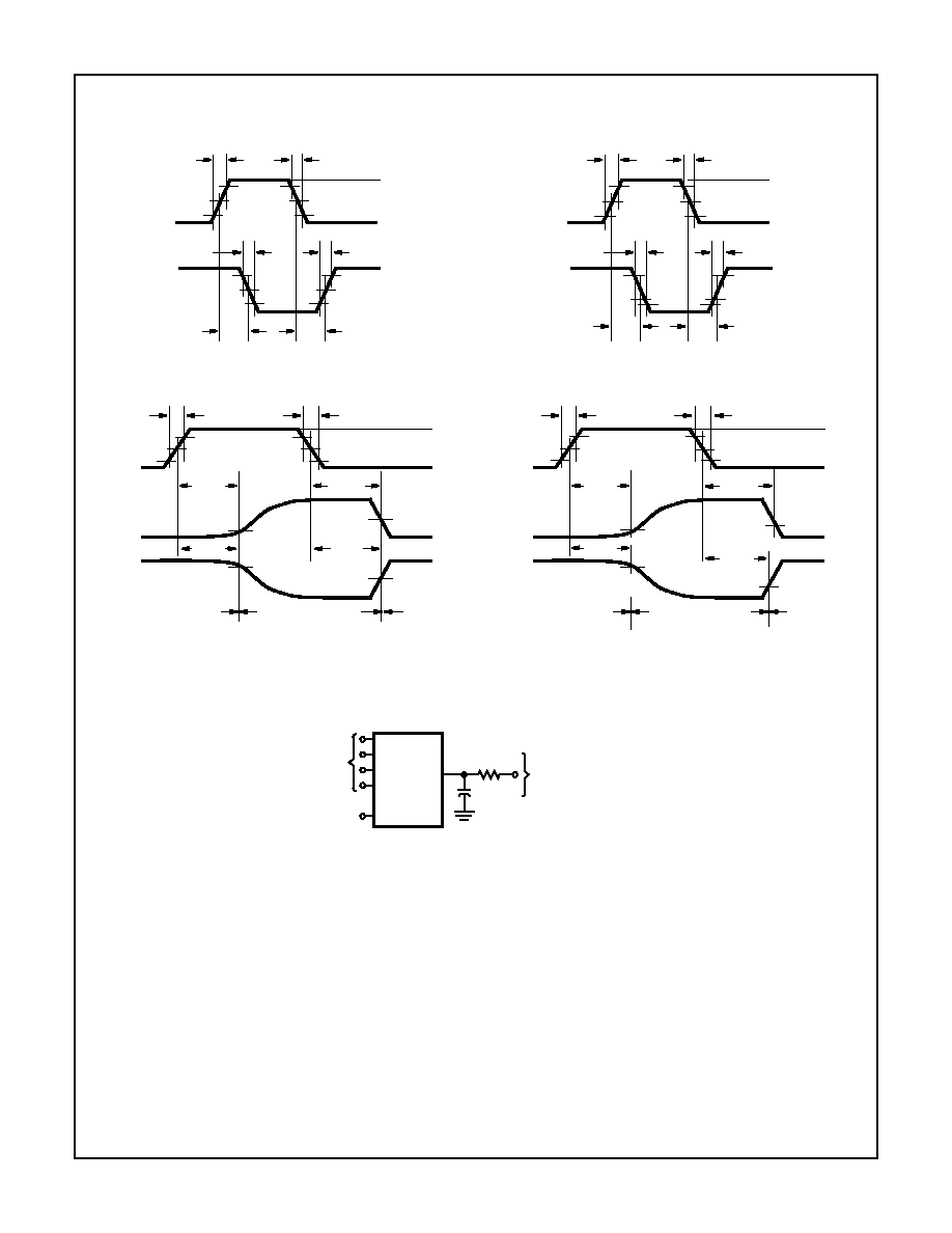
Test Circuits and Waveforms
FIGURE 1. HC AND HCT TRANSITION TIMES AND PROPAGA-
TION DELAY TIMES, COMBINATION LOGIC
FIGURE 2. HCT TRANSITION TIMES AND PROPAGATION
DELAY TIMES, COMBINATION LOGIC
FIGURE 3. HC THREE-STATE PROPAGATION DELAY
WAVEFORM
FIGURE 4. HCT THREE-STATE PROPAGATION DELAY
WAVEFORM
NOTE:
Open drain waveforms t
PLZ
and t
PZL
are the same as those for three-state shown on the left. The test circuit is Output R
L
= 1k
to
V
CC
, C
L
= 50pF.
FIGURE 5. HC AND HCT THREE-STATE PROPAGATION DELAY TEST CIRCUIT
t
PHL
t
PLH
t
THL
t
TLH
90%
50%
10%
50%
10%
INVERTING
OUTPUT
INPUT
GND
V
CC
t
r
= 6ns
t
f
= 6ns
90%
t
PHL
t
PLH
t
THL
t
TLH
2.7V
1.3V
0.3V
1.3V
10%
INVERTING
OUTPUT
INPUT
GND
3V
t
r
= 6ns
t
f
= 6ns
90%
50%
10%
90%
GND
V
CC
10%
90%
50%
50%
OUTPUT
DISABLE
OUTPUT LOW
TO OFF
OUTPUT HIGH
TO OFF
OUTPUTS
ENABLED
OUTPUTS
DISABLED
OUTPUTS
ENABLED
6ns
6ns
t
PZH
t
PHZ
t
PZL
t
PLZ
0.3
2.7
GND
3V
10%
90%
1.3V
1.3V
OUTPUT
DISABLE
OUTPUT LOW
TO OFF
OUTPUT HIGH
TO OFF
OUTPUTS
ENABLED
OUTPUTS
DISABLED
OUTPUTS
ENABLED
t
r
6ns
t
PZH
t
PHZ
t
PZL
t
PLZ
6ns
t
f
1.3
IC WITH
THREE-
STATE
OUTPUT
OTHER
INPUTS
TIED HIGH
OR LOW
OUTPUT
DISABLE
V
CC
FOR t
PLZ
AND t
PZL
GND FOR t
PHZ
AND t
PZH
OUTPUT
R
L
= 1k
C
L
50pF
CD54HC243, CD74HC243, CD54HCT243, CD74HCT243
PACKAGING INFORMATION
Orderable Device
Status
(1)
Package
Type
Package
Drawing
Pins Package
Qty
Eco Plan
(2)
Lead/Ball Finish
MSL Peak Temp
(3)
8409001CA
ACTIVE
CDIP
J
14
1
TBD
Call TI
N / A for Pkg Type
CD54HC243F
ACTIVE
CDIP
J
14
1
TBD
Call TI
N / A for Pkg Type
CD54HC243F3A
ACTIVE
CDIP
J
14
1
TBD
Call TI
N / A for Pkg Type
CD54HCT243F3A
ACTIVE
CDIP
J
14
1
TBD
Call TI
N / A for Pkg Type
CD74HC243E
ACTIVE
PDIP
N
14
25
Pb-Free
(RoHS)
CU NIPDAU
N / A for Pkg Type
CD74HC243EE4
ACTIVE
PDIP
N
14
25
Pb-Free
(RoHS)
CU NIPDAU
N / A for Pkg Type
CD74HC243M
ACTIVE
SOIC
D
14
50
Green (RoHS &
no Sb/Br)
CU NIPDAU
Level-1-260C-UNLIM
CD74HC243M96
ACTIVE
SOIC
D
14
2500 Green (RoHS &
no Sb/Br)
CU NIPDAU
Level-1-260C-UNLIM
CD74HC243M96E4
ACTIVE
SOIC
D
14
2500 Green (RoHS &
no Sb/Br)
CU NIPDAU
Level-1-260C-UNLIM
CD74HC243ME4
ACTIVE
SOIC
D
14
50
Green (RoHS &
no Sb/Br)
CU NIPDAU
Level-1-260C-UNLIM
CD74HC243MT
ACTIVE
SOIC
D
14
250
Green (RoHS &
no Sb/Br)
CU NIPDAU
Level-1-260C-UNLIM
CD74HC243MTE4
ACTIVE
SOIC
D
14
250
Green (RoHS &
no Sb/Br)
CU NIPDAU
Level-1-260C-UNLIM
CD74HCT243E
ACTIVE
PDIP
N
14
25
Pb-Free
(RoHS)
CU NIPDAU
N / A for Pkg Type
CD74HCT243EE4
ACTIVE
PDIP
N
14
25
Pb-Free
(RoHS)
CU NIPDAU
N / A for Pkg Type
CD74HCT243M
ACTIVE
SOIC
D
14
50
Green (RoHS &
no Sb/Br)
CU NIPDAU
Level-1-260C-UNLIM
CD74HCT243ME4
ACTIVE
SOIC
D
14
50
Green (RoHS &
no Sb/Br)
CU NIPDAU
Level-1-260C-UNLIM
(1)
The marketing status values are defined as follows:
ACTIVE: Product device recommended for new designs.
LIFEBUY: TI has announced that the device will be discontinued, and a lifetime-buy period is in effect.
NRND: Not recommended for new designs. Device is in production to support existing customers, but TI does not recommend using this part in
a new design.
PREVIEW: Device has been announced but is not in production. Samples may or may not be available.
OBSOLETE: TI has discontinued the production of the device.
(2)
Eco Plan - The planned eco-friendly classification: Pb-Free (RoHS), Pb-Free (RoHS Exempt), or Green (RoHS & no Sb/Br) - please check
http://www.ti.com/productcontent
for the latest availability information and additional product content details.
TBD: The Pb-Free/Green conversion plan has not been defined.
Pb-Free (RoHS): TI's terms "Lead-Free" or "Pb-Free" mean semiconductor products that are compatible with the current RoHS requirements
for all 6 substances, including the requirement that lead not exceed 0.1% by weight in homogeneous materials. Where designed to be soldered
at high temperatures, TI Pb-Free products are suitable for use in specified lead-free processes.
Pb-Free (RoHS Exempt): This component has a RoHS exemption for either 1) lead-based flip-chip solder bumps used between the die and
package, or 2) lead-based die adhesive used between the die and leadframe. The component is otherwise considered Pb-Free (RoHS
compatible) as defined above.
Green (RoHS & no Sb/Br): TI defines "Green" to mean Pb-Free (RoHS compatible), and free of Bromine (Br) and Antimony (Sb) based flame
retardants (Br or Sb do not exceed 0.1% by weight in homogeneous material)
(3)
MSL, Peak Temp. -- The Moisture Sensitivity Level rating according to the JEDEC industry standard classifications, and peak solder
temperature.
PACKAGE OPTION ADDENDUM
www.ti.com
6-Feb-2006
Addendum-Page 1

Important Information and Disclaimer:The information provided on this page represents TI's knowledge and belief as of the date that it is
provided. TI bases its knowledge and belief on information provided by third parties, and makes no representation or warranty as to the
accuracy of such information. Efforts are underway to better integrate information from third parties. TI has taken and continues to take
reasonable steps to provide representative and accurate information but may not have conducted destructive testing or chemical analysis on
incoming materials and chemicals. TI and TI suppliers consider certain information to be proprietary, and thus CAS numbers and other limited
information may not be available for release.
In no event shall TI's liability arising out of such information exceed the total purchase price of the TI part(s) at issue in this document sold by TI
to Customer on an annual basis.
PACKAGE OPTION ADDENDUM
www.ti.com
6-Feb-2006
Addendum-Page 2


IMPORTANT NOTICE
Texas Instruments Incorporated and its subsidiaries (TI) reserve the right to make corrections, modifications,
enhancements, improvements, and other changes to its products and services at any time and to discontinue
any product or service without notice. Customers should obtain the latest relevant information before placing
orders and should verify that such information is current and complete. All products are sold subject to TI's terms
and conditions of sale supplied at the time of order acknowledgment.
TI warrants performance of its hardware products to the specifications applicable at the time of sale in
accordance with TI's standard warranty. Testing and other quality control techniques are used to the extent TI
deems necessary to support this warranty. Except where mandated by government requirements, testing of all
parameters of each product is not necessarily performed.
TI assumes no liability for applications assistance or customer product design. Customers are responsible for
their products and applications using TI components. To minimize the risks associated with customer products
and applications, customers should provide adequate design and operating safeguards.
TI does not warrant or represent that any license, either express or implied, is granted under any TI patent right,
copyright, mask work right, or other TI intellectual property right relating to any combination, machine, or process
in which TI products or services are used. Information published by TI regarding third-party products or services
does not constitute a license from TI to use such products or services or a warranty or endorsement thereof.
Use of such information may require a license from a third party under the patents or other intellectual property
of the third party, or a license from TI under the patents or other intellectual property of TI.
Reproduction of information in TI data books or data sheets is permissible only if reproduction is without
alteration and is accompanied by all associated warranties, conditions, limitations, and notices. Reproduction
of this information with alteration is an unfair and deceptive business practice. TI is not responsible or liable for
such altered documentation.
Resale of TI products or services with statements different from or beyond the parameters stated by TI for that
product or service voids all express and any implied warranties for the associated TI product or service and
is an unfair and deceptive business practice. TI is not responsible or liable for any such statements.
Following are URLs where you can obtain information on other Texas Instruments products and application
solutions:
Products
Applications
Amplifiers
amplifier.ti.com
Audio
www.ti.com/audio
Data Converters
dataconverter.ti.com
Automotive
www.ti.com/automotive
DSP
dsp.ti.com
Broadband
www.ti.com/broadband
Interface
interface.ti.com
Digital Control
www.ti.com/digitalcontrol
Logic
logic.ti.com
Military
www.ti.com/military
Power Mgmt
power.ti.com
Optical Networking
www.ti.com/opticalnetwork
Microcontrollers
microcontroller.ti.com
Security
www.ti.com/security
Telephony
www.ti.com/telephony
Video & Imaging
www.ti.com/video
Wireless
www.ti.com/wireless
Mailing Address:
Texas Instruments
Post Office Box 655303 Dallas, Texas 75265
Copyright 2006, Texas Instruments Incorporated