 | –≠–ª–µ–∫—Ç—Ä–æ–Ω–Ω—ã–π –∫–æ–º–ø–æ–Ω–µ–Ω—Ç: DRV590DWP | –°–∫–∞—á–∞—Ç—å:  PDF PDF  ZIP ZIP |
Document Outline
- FEATURES
- APPLICATIONS
- DESCRIPTION
- Terminal Functions
- absolute maximum ratings over operating free-air temperature range (unl\
ess otherwise noted)
- recommended operating conditions
- ˛ˇ
- ˛ˇ
- functional block diagram
- TYPICAL CHARACTERISTICS
- APPLICATION INFORMATION
- driving TEC elements
- output filter considerations
- filter component selection
- LC filter in the frequency domain
- LC filter in the time domain
- general operation
- oscillator components R OSC and C OSC
- AREF capacitor
- gain settings
- input configurationÑdifferential and single-ended
- power supply decoupling
- SHUTDOWN operation
- power dissipation and maximum ambient temperature
- maximum output current vs duty cycle
- MECHANICAL DATA
- DWP (R-PDSO-G20) PowerPad PLASTIC SMALL-OUTLINE PACKAGE
- GQC (S-PBGA-N48) PLASTIC BALL GRID ARRAY
- IMPORTANT NOTICE
DRV590
SLOS365A ≠ AUGUST 2001 ≠ REVISED AUGUST 2002
1.2-A HIGH-EFFICIENCY PWM POWER DRIVER
1
www.ti.com
FEATURES
D
1.22-A DC (82% Duty Cycle) Output Current
(T
J
89
∞
C)
D
1-A DC (100% Duty Cycle) Output Current
(T
J
89
∞
C)
D
Low Supply Voltage Operation from 2.7 V
to 5.5 V
D
High Efficiency Generates Less Heat
D
Over-Temperature Protection
D
Short-Circuit Protection
D
PowerPAD
t
SOIC and 4
◊
4 mm MicroStar
Junior
Packages
APPLICATIONS
D
Thermoelectric Cooler (TEC) Driver
D
Laser Diode Biasing
DESCRIPTION
The DRV590 is a high-efficiency power amplifier ideal
for driving a wide variety of thermoelectric cooler
elements in systems powered from 2.7 V to 5.5 V. PWM
operation and low output stage on-resistance
significantly decrease power dissipation in the amplifier.
The DRV590 is internally protected against over
temperature conditions and current overloads due to
short circuits. The over temperature protection
activates at a junction temperature of 190
∞
C and will
deactivate once the temperature is less than 130
∞
C. If
the overcurrent circuitry is tripped, the amplifier will
automatically reset after 3≠5 ms.
The gain of the DRV590 is controlled by two input
terminals, GAIN1 and GAIN0. The amplifier may be
configured for a gain of 6, 12, 18, and 23.5 dB.
NC
IN+
IN≠
SHUTDOWN
GAIN0
GAIN1
OUT+
NC
PGND
NC
AREF
AGND
COSC
ROSC
OUT≠
NC
PGND
C6
C7
C5
L1
L2
C1
C2
C9
220 pF
R6
C4
R5
C3
R4
J2
J3
R3
J1
R2
R1
J6
OUT≠
J7
OUT+
J9
GND
J8
VDD
J4
IN+
J5
IN≠ (VCOM)
C8
120 k
120 k
1 k
1 k
120 k
1
µ
F
10
µ
F
10
µ
H
10
µ
F
10
µ
H
10
µ
F
1
µ
F
1
µ
F
10
µ
F
120 k
1
µ
F
PVDD
VDD
PVDD
J8
VDD
Typical Circuit Schematic for Driving a Thermoelectric Cooler Element
This document contains information on products in more than one phase
of development. The status of each device is indicated on the page(s)
specifying its electrical characteristics.
PowerPAD and MicroStar Junior are trademarks of Texas Instruments.
Copyright
2002, Texas Instruments Incorporated
Please be aware that an important notice concerning availability, standard warranty, and use in critical applications of
Texas Instruments semiconductor products and disclaimers thereto appears at the end of this data sheet.
DRV590
SLOS365A ≠ AUGUST 2001 ≠ REVISED AUGUST 2002
2
www.ti.com
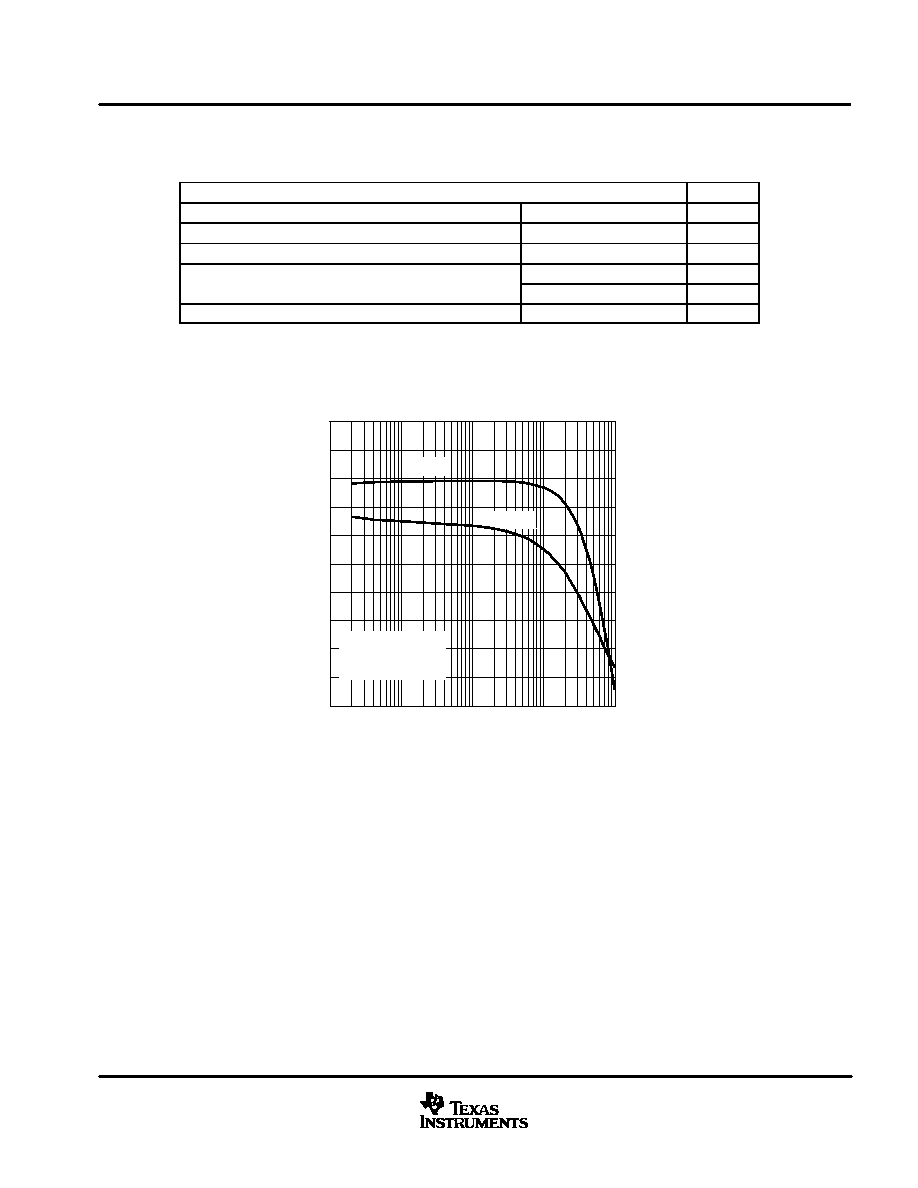
AVAILABLE OPTIONS
T
PACKAGED DEVICES
TA
SOIC (DWP)
GQC
≠ 40
∞
C to 85
∞
C
DRV590DWP
DRV590GQCR
The PW package is available taped and reeled. To order a taped and
reeled part, add the suffix R to the part number (e.g., DRV590PWR).
The GQC package is only available taped and reeled.
1
2
3
4
5
6
7
8
9
10
20
19
18
17
16
15
14
13
12
11
NC
IN+
IN≠
SHUTDOWN
GAIN0
GAIN1
PV
DD
OUT+
NC
PGND
NC
AREF
AGND
COSC
ROSC
V
DD
PV
DD
OUT≠
NC
PGND
DWP PACKAGE
(TOP VIEW)
NC ≠ No internal connection
MicroStar Junior
t
(GQC) Package
(TOP VIEW)
AGND
PVDD
IN≠
IN+
NOTE: The shaded terminals are used for thermal connections
to the ground plane.
AREF
COSC
OUT≠
PGND
NC
ROSC
VDD
PVDD
PVDD
SHUTDOWN
GAIN0
GAIN1
PVDD
OUT+
(SIDE VIEW)
NC ≠ No internal connection
A1
B1
C1
D1
E1
F1
G1
A7
B7
C7
D7
E7
F7
G7
A2
A6
Terminal Functions
TERMINAL
I/O
DESCRIPTION
NAME
GQC NO.
DWP NO.
I/O
DESCRIPTION
AGND
A3≠A5, B2≠B6
C2≠C6, D2≠D4
18
I
Analog ground
AREF
A6
19
O
Connect capacitor to ground for AREF voltage filtering (1
µ
F).
COSC
B7
17
I
Connect capacitor to ground to set oscillation frequency (220 pF).
GAIN0
C1
5
I
Bit 0 of gain control (TTL logic level)
GAIN1
D1
6
I
Bit 1 of gain control (TTL logic level)
IN≠
A1
3
I
Negative differential input
IN+
A2
2
I
Positive differential input
NC
A7
1, 9, 12, 20
Not connected
OUT≠
G7
13
O
Negative BTL output
OUT+
G1
8
O
Positive BTL output
PGND
D5≠D6, E2≠E6
F2≠F6, G2≠G6
10, 11
I
High-current grounds (2)
PVDD
E1, E7, F1, F7
7, 14
I
High-current power supplies (2)
ROSC
C7
16
I
Connect resistor to ground to set oscillation frequency (120 k
).
SHUTDOWN
B1
4
I
Places the amplifier in shutdown mode if a TTL logic low is placed on this terminal,
and normal operation if a TTL logic high is placed on this terminal.
VDD
D7
15
I
Analog power supply
DRV590
SLOS365A ≠ AUGUST 2001 ≠ REVISED AUGUST 2002
3
www.ti.com
absolute maximum ratings over operating free-air temperature range (unless otherwise noted)
Supply voltage, V
DD,
PV
DD
≠0.3 V to 5.5 V
. . . . . . . . . . . . . . . . . . . . . . . . . . . . . . . . . . . . . . . . . . . . . . . . . . . . . . . . . . . . .
Input voltage, V
I
≠0.3 V to V
DD
+ 0.3 V
. . . . . . . . . . . . . . . . . . . . . . . . . . . . . . . . . . . . . . . . . . . . . . . . . . . . . . . . . . . . . . . . . .
Continuous total power dissipation
See Dissipation Rating Table
. . . . . . . . . . . . . . . . . . . . . . . . . . . . . . . . . . . . . . . . . .
Operating free-air temperature range, T
A
≠ 40
∞
C to 85
∞
C
. . . . . . . . . . . . . . . . . . . . . . . . . . . . . . . . . . . . . . . . . . . . . . . . . .
Operating junction temperature range, T
J
≠ 40
∞
C to 150
∞
C
. . . . . . . . . . . . . . . . . . . . . . . . . . . . . . . . . . . . . . . . . . . . . . . .
Storage temperature range, T
stg
≠65
∞
C to 150
∞
C
. . . . . . . . . . . . . . . . . . . . . . . . . . . . . . . . . . . . . . . . . . . . . . . . . . . . . . . .
Lead temperature 1,6 mm (1/16 inch) from case for 10 seconds
260
∞
C
. . . . . . . . . . . . . . . . . . . . . . . . . . . . . . . . . . . . .
Stresses beyond those listed under "absolute maximum ratings" may cause permanent damage to the device. These are stress ratings only, and
functional operation of the device at these or any other conditions beyond those indicated under "recommended operating conditions" is not
implied. Exposure to absolute-maximum-rated conditions for extended periods may affect device reliability.
DISSIPATION RATING TABLE
PACKAGE
TA
25
∞
C
DERATING FACTOR
TA = 70
∞
C
TA = 85
∞
C
GQC
2.61 W
20.9 mW/
∞
C
1.67 W
1.36 W
DWP
3.66 W
29.3 mW/
∞
C
2.34 W
1.9 W
recommended operating conditions
MIN
MAX
UNIT
¡¡¡¡¡¡¡¡¡¡¡¡¡¡¡¡¡¡¡¡¡¡¡¡¡¡¡
Supply voltage, VDD, PVDD
¡¡¡
2.7
¡¡¡
5.5
¡¡¡
V
¡¡¡¡¡¡¡¡¡¡¡¡¡¡¡¡¡¡
¡¡¡¡¡¡¡¡¡¡¡¡¡¡¡¡¡¡
High-level input voltage, VIH
¡¡¡¡¡¡¡¡¡¡
¡¡¡¡¡¡¡¡¡¡
GAIN0, GAIN1, SHUTDOWN
¡¡¡
¡¡¡
2
¡¡¡
¡¡¡
¡¡¡
¡¡¡
V
¡¡¡¡¡¡¡¡¡¡¡¡¡¡¡¡¡¡
¡¡¡¡¡¡¡¡¡¡¡¡¡¡¡¡¡¡
Low-level input voltage, VIL
¡¡¡¡¡¡¡¡¡¡
¡¡¡¡¡¡¡¡¡¡
GAIN0, GAIN1, SHUTDOWN
¡¡¡
¡¡¡
¡¡¡
¡¡¡
0.7
¡¡¡
¡¡¡
V
¡¡¡¡¡¡¡¡¡¡¡¡¡¡¡¡¡¡¡¡¡¡¡¡¡¡¡
¡¡¡¡¡¡¡¡¡¡¡¡¡¡¡¡¡¡¡¡¡¡¡¡¡¡¡
Operating free-air temperature, TA
¡¡¡
¡¡¡
≠ 40
¡¡¡
¡¡¡
85
¡¡¡
¡¡¡
∞
C
Load impedance
1
electrical characteristics at specified free-air temperature, T
A
= 25
∞
C (unless otherwise noted)
PARAMETER
TEST CONDITIONS
MIN
TYP
MAX
UNIT
¡¡¡
¡¡¡
¡¡¡
|VOS|
¡¡¡¡¡¡¡¡¡
¡¡¡¡¡¡¡¡¡
¡¡¡¡¡¡¡¡¡
Output offset voltage (measured
differentially)
¡¡¡¡¡¡¡¡¡¡¡
¡¡¡¡¡¡¡¡¡¡¡
¡¡¡¡¡¡¡¡¡¡¡
VI = 0 V,
AV = any gain
¡¡¡
¡¡¡
¡¡¡
¡¡¡
¡¡¡
¡¡¡
¡¡¡
¡¡¡
¡¡¡
25
¡¡¡
¡¡¡
¡¡¡
mV
¡¡¡
PSRR
¡¡¡¡¡¡¡¡¡
Power supply rejection ratio
¡¡¡¡¡¡¡¡¡¡¡
PVDD = 4.9 V to 5.1 V
¡¡¡
¡¡¡
77
¡¡¡
¡¡¡
dB
¡¡¡
¡¡¡
PSRR
¡¡¡¡¡¡¡¡¡
¡¡¡¡¡¡¡¡¡
Power supply rejection ratio
¡¡¡¡¡¡¡¡¡¡¡
¡¡¡¡¡¡¡¡¡¡¡
PVDD = 3.2 V to 3.4 V
¡¡¡
¡¡¡
¡¡¡
¡¡¡
61
¡¡¡
¡¡¡
¡¡¡
¡¡¡
dB
¡¡¡
¡¡¡
|IIH|
¡¡¡¡¡¡¡¡¡
¡¡¡¡¡¡¡¡¡
High-level input current
¡¡¡¡¡¡¡¡¡¡¡
¡¡¡¡¡¡¡¡¡¡¡
VI = 3.3 V
¡¡¡
¡¡¡
¡¡¡
¡¡¡
¡¡¡
¡¡¡
1
¡¡¡
¡¡¡
µ
A
¡¡¡
¡¡¡
|IIL|
¡¡¡¡¡¡¡¡¡
¡¡¡¡¡¡¡¡¡
Low-level input current
¡¡¡¡¡¡¡¡¡¡¡
¡¡¡¡¡¡¡¡¡¡¡
VI = 0 V
¡¡¡
¡¡¡
¡¡¡
¡¡¡
¡¡¡
¡¡¡
1
¡¡¡
¡¡¡
µ
A
¡¡¡
¡¡¡
IDD
¡¡¡¡¡¡¡¡¡
¡¡¡¡¡¡¡¡¡
Supply current, no filter
¡¡¡¡¡¡¡¡¡¡¡
¡¡¡¡¡¡¡¡¡¡¡
¡¡¡
¡¡¡
¡¡¡
¡¡¡
4.5
¡¡¡
¡¡¡
6.5
¡¡¡
¡¡¡
mA
¡¡¡
¡¡¡
IDD(SD)
¡¡¡¡¡¡¡¡¡
¡¡¡¡¡¡¡¡¡
Supply current, shutdown mode
¡¡¡¡¡¡¡¡¡¡¡
¡¡¡¡¡¡¡¡¡¡¡
GAIN0, GAIN1, SHUTDOWN = 0 V
¡¡¡
¡¡¡
¡¡¡
¡¡¡
0.05
¡¡¡
¡¡¡
5
¡¡¡
¡¡¡
µ
A
¡¡¡
¡¡¡
¡¡¡¡¡¡¡¡¡
¡¡¡¡¡¡¡¡¡
¡¡¡¡¡¡¡¡¡¡¡
¡¡¡¡¡¡¡¡¡¡¡
GAIN0 = low, GAIN1 = low
¡¡¡
¡¡¡
5.1
¡¡¡
¡¡¡
6
¡¡¡
¡¡¡
6.5
¡¡¡
¡¡¡
¡¡¡
¡¡¡
¡¡¡¡¡¡¡¡¡
¡¡¡¡¡¡¡¡¡
Gain
GAIN0 = high, GAIN1 = low
¡¡¡
¡¡¡
11
¡¡¡
¡¡¡
12
¡¡¡
¡¡¡
12.5
¡¡¡
¡¡¡
dB
¡¡¡
¡¡¡
¡¡¡¡¡¡¡¡¡
¡¡¡¡¡¡¡¡¡
Gain
GAIN0 = low, GAIN1 = high
¡¡¡
¡¡¡
17
¡¡¡
¡¡¡
18
¡¡¡
¡¡¡
19
¡¡¡
¡¡¡
dB
¡¡¡
¡¡¡¡¡¡¡¡¡
GAIN0 = high, GAIN1 = high
¡¡¡
23
¡¡¡
23.5
¡¡¡
24
¡¡¡
f
Switching frequency
Single ended
R
120 k
C
220 pF
¡¡¡
¡¡¡
¡¡¡
¡¡¡
250
¡¡¡
¡¡¡
¡¡¡
¡¡¡
kHz
fs
Switching frequency
Differential
Rosc = 120 k
, Cosc = 220 pF
¡¡¡
¡¡¡
¡¡¡
¡¡¡
500
¡¡¡
¡¡¡
¡¡¡
¡¡¡
kHz
DRV590
SLOS365A ≠ AUGUST 2001 ≠ REVISED AUGUST 2002
4
www.ti.com
operating characteristics, T
A
= 25
∞
C, R
L
= 2
,
gain = 6 dB (unless otherwise noted)
PARAMETER
TEST CONDITIONS
MIN
TYP
MAX
UNIT
¡¡¡¡
¡¡¡¡
IO
¡¡¡¡¡¡¡¡¡¡¡¡
¡¡¡¡¡¡¡¡¡¡¡¡
Maximum output current
¡¡¡¡¡¡
¡¡¡¡¡¡
Duty cycle = 82%
¡¡¡¡¡¡¡
¡¡¡¡¡¡¡
¡¡
¡¡
¡¡¡
¡¡¡
1.22
¡¡¡
¡¡¡
¡¡¡
¡¡¡
A
¡¡¡¡
¡¡¡¡
PSRR
¡¡¡¡¡¡¡¡¡¡¡¡
¡¡¡¡¡¡¡¡¡¡¡¡
Power supply rejection ratio
¡¡¡¡¡¡
¡¡¡¡¡¡
f = 1 kHz,
¡¡¡¡¡¡¡
¡¡¡¡¡¡¡
C(AREF) = 1
µ
F
¡¡
¡¡
¡¡¡
¡¡¡
70
¡¡¡
¡¡¡
¡¡¡
¡¡¡
dB
¡¡¡¡
¡¡¡¡
ZI
¡¡¡¡¡¡¡¡¡¡¡¡
¡¡¡¡¡¡¡¡¡¡¡¡
Input impedance
¡¡¡¡¡¡
¡¡¡¡¡¡
¡¡¡¡¡¡¡
¡¡¡¡¡¡¡
¡¡
¡¡
¡¡¡
¡¡¡
>
15
¡¡¡
¡¡¡
¡¡¡
¡¡¡
k
V
Common mode input voltage range
PVDD = 5 V
1.2
3.8
V
VICR
Common-mode input voltage range
PVDD = 3.3 V
1.2
2.1
V
r
Output on resistance
PVDD = 5 V
0.5
rds(on)
Output on-resistance
PVDD = 3.3 V
0.65
Efficiency
PVDD = 5 V
64%
Efficiency
PVDD = 3.3 V
60%
Vn
Integrated noise floor
f = 10 Hz to 5 kHz, Gain = 6 dB
23
µ
V rms
functional block diagram
Gate
Drive
_
+
Gate
Drive
_
+
_
+
_
+
Gain
Adjust
Gain
Adjust
Start-Up
Protection
Logic
OC
Detect
Thermal
VDD ok
Ramp
Generator
Biases
and
References
Gain
2
AGND
VDD
VDD
PVDD
IN≠
OUT≠
PGND
PVDD
OUT+
PGND
IN+
SHUTDOWN
GAIN1
GAIN0
COSC
ROSC
AREF
SD
_
+
_
+
Deglitch
Logic
Deglitch
Logic
DRV590
SLOS365A ≠ AUGUST 2001 ≠ REVISED AUGUST 2002
5
www.ti.com
TYPICAL CHARACTERISTICS
Table of Graphs
FIGURE
Gain and phase
vs Frequency
1
Efficiency
vs Load resistance
2, 3
PSRR
Power supply rejection ratio
vs Frequency
4
r
Small signal drain source on state resistance
vs Supply voltage
5, 6
rds(on)
Small-signal drain-source on-state resistance
vs Ambient temperature
7, 8
IO
Maximum output current
vs Differential output voltage
9
≠180
≠152
≠124
≠96
≠68
≠40
≠12
16
44
72
100
f ≠ Frequency ≠ Hz
≠10
≠8
≠6
≠4
≠2
0
2
4
6
8
10
VI = 1.17 Vrms
VDD = 5 V
RL = 2
GAIN AND PHASE
vs
FREQUENCY
Phase
Gain
Gain
≠
dBV
Phase
≠
∞
10
100
1k
100k
10k
Figure 1