 | –≠–ª–µ–∫—Ç—Ä–æ–Ω–Ω—ã–π –∫–æ–º–ø–æ–Ω–µ–Ω—Ç: LF411D | –°–∫–∞—á–∞—Ç—å:  PDF PDF  ZIP ZIP |

LF411
JFET-INPUT OPERATIONAL AMPLIFIER
SLOS011C ≠ MARCH 1987 ≠ REVISED OCTOBER 1997
1
POST OFFICE BOX 655303
∑
DALLAS, TEXAS 75265
D
Low Input Bias Current, 50 pA Typ
D
Low Input Noise Current, 0.01 pA/
Hz Typ
D
Low Supply Current, 2 mA Typ
D
High Input impedance, 10
12
Typ
D
Low Total Harmonic Distortion
D
Low 1/f Noise Corner, 50 Hz Typ
D
Package Options Include Plastic
Small-Outline (D) and Standard (P) DIPs
description
This device is a low-cost, high-speed, JFET-input operational amplifier with very low input offset voltage and
a maximum input offset voltage drift. It requires low supply current, yet maintains a large gain-bandwidth product
and a fast slew rate. In addition, the matched high-voltage JFET input provides very low input bias and offset
currents.
The LF411 can be used in applications such as high-speed integrators, digital-to-analog converters,
sample-and-hold circuits, and many other circuits.
The LF411C is characterized for operation from 0
∞
C to 70
∞
C. The LF411I is characterized for operation from
≠40
∞
C to 85
∞
C.
symbol
≠
+
IN ≠
IN +
OUT
BAL1
BAL2
2
3
1
5
6
AVAILABLE OPTIONS
VIOmax
PACKAGE
TA
VIOmax
AT 25
∞
C
SMALL OUTLINE
(D)
PLASTIC DIP
(P)
0
∞
C to 70
∞
C
2 mV
LF411CD
LF411CP
≠40
∞
C to 85
∞
C
2 mV
LF411ID
LF411IP
The D packages are available taped and reeled. Add the suffix R to the
device type (i.e., LF411CDR).
Copyright
©
1997, Texas Instruments Incorporated
PRODUCTION DATA information is current as of publication date.
Products conform to specifications per the terms of Texas Instruments
standard warranty. Production processing does not necessarily include
testing of all parameters.
1
2
3
4
8
7
6
5
BAL1
IN ≠
IN +
V
CC ≠
NC
V
CC +
OUT
BAL2
D OR P PACKAGE
(TOP VIEW)
NC ≠ No internal connection
Please be aware that an important notice concerning availability, standard warranty, and use in critical applications of
Texas Instruments semiconductor products and disclaimers thereto appears at the end of this data sheet.

LF411
JFET-INPUT OPERATIONAL AMPLIFIER
SLOS011C ≠ MARCH 1987 ≠ REVISED OCTOBER 1997
2
POST OFFICE BOX 655303
∑
DALLAS, TEXAS 75265
absolute maximum ratings over operating free-air temperature range (unless otherwise noted)
Supply voltage, V
CC +
18 V
. . . . . . . . . . . . . . . . . . . . . . . . . . . . . . . . . . . . . . . . . . . . . . . . . . . . . . . . . . . . . . . . . . . . . .
Supply voltage, V
CC ≠
≠ 18 V
. . . . . . . . . . . . . . . . . . . . . . . . . . . . . . . . . . . . . . . . . . . . . . . . . . . . . . . . . . . . . . . . . . . . .
Differential input voltage, V
ID
±
30 V
. . . . . . . . . . . . . . . . . . . . . . . . . . . . . . . . . . . . . . . . . . . . . . . . . . . . . . . . . . . . . . .
Input voltage, V
I
(see Note 1)
±
15 V
. . . . . . . . . . . . . . . . . . . . . . . . . . . . . . . . . . . . . . . . . . . . . . . . . . . . . . . . . . . . . . .
Duration of output short circuit
Unlimited
. . . . . . . . . . . . . . . . . . . . . . . . . . . . . . . . . . . . . . . . . . . . . . . . . . . . . . . . . . .
Continuous total power dissipation
500 mW
. . . . . . . . . . . . . . . . . . . . . . . . . . . . . . . . . . . . . . . . . . . . . . . . . . . . . . . .
Package thermal impedance,
JA
(see Note 2): D package
197
∞
C/W
. . . . . . . . . . . . . . . . . . . . . . . . . . . . . . . . . .
P package
104
∞
C/W
. . . . . . . . . . . . . . . . . . . . . . . . . . . . . . . . . .
Storage temperature range, T
stg
≠ 65
∞
C to 150
∞
C
. . . . . . . . . . . . . . . . . . . . . . . . . . . . . . . . . . . . . . . . . . . . . . . . . . .
Lead temperature 1,6 mm (1/16 inch) from case for 10 seconds
260
∞
C
. . . . . . . . . . . . . . . . . . . . . . . . . . . . . . .
NOTES:
1. Unless otherwise specified, the absolute maximum negative input voltage is equal to the negative power supply voltage.
2. The package thermal impedance is calculated in accordance with JESD 51, except for through-hole packages, which use a trace
length of zero.
recommended operating conditions
C SUFFIX
I SUFFIX
UNIT
MIN
MAX
MIN
MAX
UNIT
Supply voltage, VCC +
3.5
18
3.5
18
V
Supply voltage, VCC ≠
≠ 3.5
≠ 18
≠ 3.5
≠ 18
V
Operating free-air temperature, TA
0
70
≠ 40
≠85
∞
C
electrical characteristics over operating free-air temperature range, V
CC
±
=
±
15 V (unless otherwise
specified)
PARAMETER
TEST CONDITIONS
TA
MIN
TYP
MAX
UNIT
PARAMETER
TEST CONDITIONS
LF411C
LF411I
MIN
TYP
MAX
UNIT
VIO
Input offset voltage
VIC = 0,
RS = 10 k
25
∞
C
25
∞
C
0.8
2
mV
VIO
Average temperature coeffi-
cient of input offset voltage
VIC = 0,
RS = 10 k
10
20
µ
V/
∞
C
IIO
Inp t offset c rrent
VIC = 0
25
∞
C
25
∞
C
25
100
pA
IIO
Input offset current
VIC = 0
70
∞
C
85
∞
C
2
nA
IIB
Inp t bias c rrent
VIC = 0
25
∞
C
25
∞
C
50
200
pA
IIB
Input bias current
VIC = 0
70
∞
C
85
∞
C
4
nA
VICR
Common-mode input voltage
range
±
11
≠11.5
to
14.5
V
VOM
Maximum peak output-voltage
swing
RL = 10 k
±
12
±
13.5
V
AVD
Large-signal differential
VO =
±
10 V
RL = 2 k
25
∞
C
25
∞
C
25
200
V/mV
AVD
g
g
voltage
VO =
±
10 V,
RL = 2 k
0
∞
C to 70
∞
C
≠40
∞
C to 85
∞
C
15
200
V/mV
ri
Input resistance
TJ = 25
∞
C
1012
CMR
R
Common-mode rejection ratio
RS
10 k
70
100
dB
kSVR
Supply-voltage rejection ratio
See Note 3
70
100
dB
ICC
Supply current
2
3.4
mA
At least 90% of the devices meet this limit for
VIO.
Input bias currents of an FET-input operational amplifier are normal junction reverse currents, which are temperature sensitive. Pulse techniques
must be used that will maintain the junction temperatures as close to the ambient temperature as possible.
NOTE 3: Supply-voltage rejection ratio is measured for both supply magnitudes increasing or decreasing simultaneously.

LF411
JFET-INPUT OPERATIONAL AMPLIFIER
SLOS011C ≠ MARCH 1987 ≠ REVISED OCTOBER 1997
3
POST OFFICE BOX 655303
∑
DALLAS, TEXAS 75265
operating characteristics, V
CC
±
=
±
15 V, T
A
= 25
∞
C
PARAMETER
TEST CONDITIONS
MIN
TYP
MAX
UNIT
SR
Slew rate
8
13
V/
µ
s
B1
Unity-gain bandwidth
2.7
3
MHz
Vn
Equivalent input noise voltage
f = 1 kHz,
RS = 20
18
nV/
Hz
In
Equivalent input noise current
f = 1 kHz
0.01
pA/
Hz

PACKAGING INFORMATION
Orderable Device
Status
(1)
Package
Type
Package
Drawing
Pins Package
Qty
Eco Plan
(2)
Lead/Ball Finish
MSL Peak Temp
(3)
LF411CD
ACTIVE
SOIC
D
8
75
Green (RoHS &
no Sb/Br)
CU NIPDAU
Level-1-260C-UNLIM
LF411CDE4
ACTIVE
SOIC
D
8
75
Green (RoHS &
no Sb/Br)
CU NIPDAU
Level-1-260C-UNLIM
LF411CDR
ACTIVE
SOIC
D
8
2500 Green (RoHS &
no Sb/Br)
CU NIPDAU
Level-1-260C-UNLIM
LF411CDRE4
ACTIVE
SOIC
D
8
2500 Green (RoHS &
no Sb/Br)
CU NIPDAU
Level-1-260C-UNLIM
LF411CP
ACTIVE
PDIP
P
8
50
Pb-Free
(RoHS)
CU NIPDAU
Level-NC-NC-NC
LF411CPE4
ACTIVE
PDIP
P
8
50
Pb-Free
(RoHS)
CU NIPDAU
Level-NC-NC-NC
LF411ID
OBSOLETE
SOIC
D
8
TBD
Call TI
Call TI
LF411IDR
OBSOLETE
SOIC
D
8
TBD
Call TI
Call TI
LF411IP
OBSOLETE
PDIP
P
8
TBD
Call TI
Call TI
(1)
The marketing status values are defined as follows:
ACTIVE: Product device recommended for new designs.
LIFEBUY: TI has announced that the device will be discontinued, and a lifetime-buy period is in effect.
NRND: Not recommended for new designs. Device is in production to support existing customers, but TI does not recommend using this part in
a new design.
PREVIEW: Device has been announced but is not in production. Samples may or may not be available.
OBSOLETE: TI has discontinued the production of the device.
(2)
Eco
Plan
-
The
planned
eco-friendly
classification:
Pb-Free
(RoHS)
or
Green
(RoHS
&
no
Sb/Br)
-
please
check
http://www.ti.com/productcontent
for the latest availability information and additional product content details.
TBD: The Pb-Free/Green conversion plan has not been defined.
Pb-Free (RoHS): TI's terms "Lead-Free" or "Pb-Free" mean semiconductor products that are compatible with the current RoHS requirements
for all 6 substances, including the requirement that lead not exceed 0.1% by weight in homogeneous materials. Where designed to be soldered
at high temperatures, TI Pb-Free products are suitable for use in specified lead-free processes.
Green (RoHS & no Sb/Br): TI defines "Green" to mean Pb-Free (RoHS compatible), and free of Bromine (Br) and Antimony (Sb) based flame
retardants (Br or Sb do not exceed 0.1% by weight in homogeneous material)
(3)
MSL, Peak Temp. -- The Moisture Sensitivity Level rating according to the JEDEC industry standard classifications, and peak solder
temperature.
Important Information and Disclaimer:The information provided on this page represents TI's knowledge and belief as of the date that it is
provided. TI bases its knowledge and belief on information provided by third parties, and makes no representation or warranty as to the
accuracy of such information. Efforts are underway to better integrate information from third parties. TI has taken and continues to take
reasonable steps to provide representative and accurate information but may not have conducted destructive testing or chemical analysis on
incoming materials and chemicals. TI and TI suppliers consider certain information to be proprietary, and thus CAS numbers and other limited
information may not be available for release.
In no event shall TI's liability arising out of such information exceed the total purchase price of the TI part(s) at issue in this document sold by TI
to Customer on an annual basis.
PACKAGE OPTION ADDENDUM
www.ti.com
17-Oct-2005
Addendum-Page 1
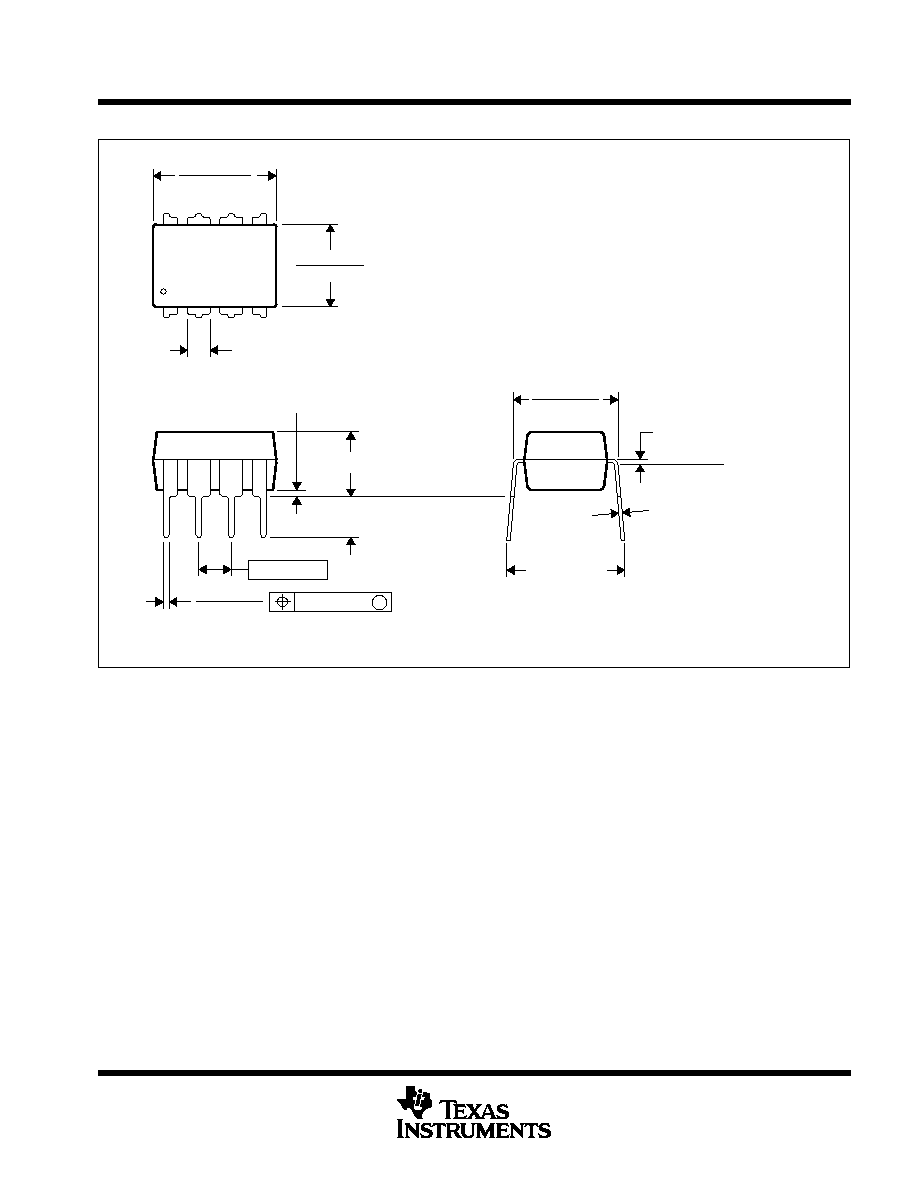
MECHANICAL DATA
MPDI001A ≠ JANUARY 1995 ≠ REVISED JUNE 1999
POST OFFICE BOX 655303
∑
DALLAS, TEXAS 75265
P (R-PDIP-T8)
PLASTIC DUAL-IN-LINE
8
4
0.015 (0,38)
Gage Plane
0.325 (8,26)
0.300 (7,62)
0.010 (0,25) NOM
MAX
0.430 (10,92)
4040082/D 05/98
0.200 (5,08) MAX
0.125 (3,18) MIN
5
0.355 (9,02)
0.020 (0,51) MIN
0.070 (1,78) MAX
0.240 (6,10)
0.260 (6,60)
0.400 (10,60)
1
0.015 (0,38)
0.021 (0,53)
Seating Plane
M
0.010 (0,25)
0.100 (2,54)
NOTES: A. All linear dimensions are in inches (millimeters).
B. This drawing is subject to change without notice.
C. Falls within JEDEC MS-001
For the latest package information, go to http://www.ti.com/sc/docs/package/pkg_info.htm