 | –≠–ª–µ–∫—Ç—Ä–æ–Ω–Ω—ã–π –∫–æ–º–ø–æ–Ω–µ–Ω—Ç: LM118 | –°–∫–∞—á–∞—Ç—å:  PDF PDF  ZIP ZIP |

LM118, LM218, LM318
FAST GENERAL-PURPOSE OPERATIONAL AMPLIFIERS
SLOS063A ≠ JUNE 1976 ≠ REVISED APRIL 1994
1
POST OFFICE BOX 655303
∑
DALLAS, TEXAS 75265
D
Small-Signal Bandwidth . . . 15 MHz Typ
D
Slew Rate . . . 50 V/
µ
s Min
D
Bias Current . . . 250 nA Max (LM118,
LM218)
D
Supply Voltage Range . . .
±
5 V to
±
20 V
D
Internal Frequency Compensation
D
Input and Output Overload Protection
D
Same Pin Assignments as
General-Purpose Operational Amplifiers
description
The LM118, LM218, and LM318 are precision,
fast operational amplifiers designed for
applications requiring wide bandwidth and high
slew rate. They feature a factor-of-ten increase in
speed over general-purpose devices without
sacrificing dc performance.
These operational amplifiers have internal unity-
gain frequency compensation. This considerably
simplifies their application, since no external
components are necessary for operation.
However, unlike most internally compensated
amplifiers, external frequency compensation may
be added for optimum performance. For inverting
applications, feed-forward compensation boosts
the slew rate to over 150 V/
µ
s and almost double
the bandwidth. Overcompensation can be used
with the amplifier for greater stability when
maximum bandwidth is not needed. Further, a
single capacitor may be added to reduce the
settling time for 0.1% error band to under 1
µ
s.
The high speed and fast settling time of these
operational amplifiers make them useful in A/D
converters, oscillators, active filters, sample-and-
hold circuits, and general-purpose amplifiers.
The LM118 is characterized for operation from
≠ 55
∞
C to 125
∞
C. The LM218 is characterized for
operation from ≠ 25
∞
C to 85
∞
C, and the LM318 is
characterized for operation from 0
∞
C to 70
∞
C.
Copyright
©
1994, Texas Instruments Incorporated
PRODUCTION DATA information is current as of publication date.
Products conform to specifications per the terms of Texas Instruments
standard warranty. Production processing does not necessarily include
testing of all parameters.
On products compliant to MIL-PRF-38535, all parameters are tested
unless otherwise noted. On all other products, production
processing does not necessarily include testing of all parameters.
1
2
3
4
8
7
6
5
BAL /COMP1
IN ≠
IN +
V
CC ≠
COMP2
V
CC +
OUT
BAL /COMP3
D, JG, OR P PACKAGE
(TOP VIEW)
3
2
1 20 19
9 10 11 12 13
4
5
6
7
8
18
17
16
15
14
NC
V
CC +
NC
OUT
NC
NC
IN ≠
NC
IN +
NC
FK PACKAGE
(TOP VIEW)
NC
BAL/COMP1
NC
NC
NC
NC
NC
NC ≠ No internal connection
CC ≠
V
BAL/COMP3
COMP2
+
≠
BAL/COMP1
COMP2
BAL/COMP3
IN +
IN ≠
OUT
symbol
1
8
5
3
2
Pin numbers shown are for the D, JG, and P packages.

LM118, LM218, LM318
FAST GENERAL-PURPOSE OPERATIONAL AMPLIFIERS
SLOS063A ≠ JUNE 1976 ≠ REVISED APRIL 1994
2
POST OFFICE BOX 655303
∑
DALLAS, TEXAS 75265
AVAILABLE OPTIONS
VIOmax
PACKAGE
TA
VIOmax
AT 25
∞
C
SMALL OUTLINE
(D)
CHIP CARRIER
(FK)
CERAMIC DIP
(JG)
PLASTIC DIP
(P)
0
∞
C to 70
∞
C
10 mV
LM318D
--
--
LM318P
≠ 25
∞
C to 85
∞
C
4 mV
LM218D
--
--
LM218P
≠ 55
∞
C to 125
∞
C
4 mV
LM118D
LM118FK
LM118JG
LM118P
The D package is available taped and reeled. Add the suffix R to the device type (e.g., LM318DR).
schematic
33
COMP2
2 k
2 k
20 k
20 k
20 k
5 k
5 k
5 k
150 k
1 k
1 k
3.5 k
13
25
30
50
4 k
500
1.2 k
1.2 k
110
5.6 k
30
1.7 k
6 pF
28 pF
100 pF
VCC +
OUT
VCC ≠
IN ≠
IN +
Component values shown are nominal.
BAL/COMP1
BAL/COMP3
LM118, LM218, LM318
FAST GENERAL-PURPOSE OPERATIONAL AMPLIFIERS
SLOS063A ≠ JUNE 1976 ≠ REVISED APRIL 1994
3
POST OFFICE BOX 655303
∑
DALLAS, TEXAS 75265
absolute maximum ratings over operating free-air temperature range (unless otherwise noted)
LM118
LM218
LM318
UNIT
Supply voltage, VCC + (see Note 1)
20
20
20
V
Supply voltage, VCC ≠ (see Note 1)
≠ 20
≠ 20
≠ 20
V
Input voltage, VI (either input, see Notes 1 and 2)
±
15
±
15
±
15
V
Differential input current, VID (see Note 3)
±
10
±
10
±
10
mA
Duration of output short circuit (see Note 4)
unlimited
unlimited
unlimited
Continuous total power dissipation
See Dissipation Rating Table
Operating free-air temperature range, TA
≠ 55 to 125
≠ 25 to 85
0 to 70
∞
C
Storage temperature range
≠ 65 to 150
≠ 65 to 150
≠ 65 to 50
∞
C
Case temperature for 60 seconds
FK package
260
∞
C
Lead temperature 1,6 mm (1/16 inch) from case for 10 seconds
D or P package
260
260
260
∞
C
Lead temperature 1,6 mm (1/16 inch) from case for 60 seconds
JG package
300
∞
C
NOTES:
1. All voltage values, unless otherwise noted, are with respect to the midpoint between VCC + and VCC ≠ .
2. The magnitude of the input voltage must never exceed the magnitude of the supply voltage or 15 V, whichever is less.
3. The inputs are shunted with two opposite-facing base-emitter diodes for overvoltage protection. Therefore, excessive current flows
if a different input voltage in excess of approximately 1 V is applied between the inputs unless some limiting resistance is used.
4. The output can be shorted to ground or either power supply. For the LM118 and LM218 only, the unlimited duration of the short circuit
applies at (or below) 85
∞
C case temperature or 75
∞
C free-air temperature.
DISSIPATION RATING TABLE
PACKAGE
TA
25
∞
C
DERATING
DERATE
TA = 70
∞
C
TA = 85
∞
C
TA = 125
∞
C
PACKAGE
A
POWER RATING
FACTOR
ABOVE TA
A
POWER RATING
A
POWER RATING
A
POWER RATING
D
500 mV
5.8 mW/
∞
C
64
∞
C
464 mW
377 mW
145 mW
FK
500 mV
11.0 mW/
∞
C
105
∞
C
500 mW
500 mW
275 mW
JG
500 mV
8.4 mW/
∞
C
90
∞
C
500 mW
500 mW
210 mW
P
500 mV
8.0 mW/
∞
C
88
∞
C
500 mW
500 mW
200 mW

LM118, LM218, LM318
FAST GENERAL-PURPOSE OPERATIONAL AMPLIFIERS
SLOS063A ≠ JUNE 1976 ≠ REVISED APRIL 1994
4
POST OFFICE BOX 655303
∑
DALLAS, TEXAS 75265
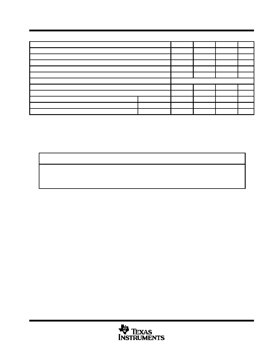
electrical characteristics at specified free-air temperature (see Note 5)
PARAMETER
TEST
T
LM118, LM218
LM318
UNIT
PARAMETER
TEST
CONDITIONS
TA
MIN
TYP
MAX
MIN
TYP
MAX
UNIT
VIO
Input offset voltage
VO = 0
25
∞
C
2
4
4
10
mV
VIO
Input offset voltage
VO = 0
Full range
6
15
mV
IIO
Input offset current
VO = 0
25
∞
C
6
50
30
200
nA
IIO
Input offset current
VO = 0
Full range
100
300
nA
IIB
Input bias current
VO = 0
25
∞
C
120
250
150
500
nA
IIB
Input bias current
VO = 0
Full range
500
750
nA
VICR
Common-mode input voltage range
VCC
±
=
±
15 V
Full range
±
11.5
±
11.5
V
VOM
Maximum peak output voltage
swing
VCC
±
=
±
15 V,
RL = 2 k
Full range
±
12
±
13
±
12
±
13
V
AVD
Large-signal differential
VCC
±
=
±
15 V,
VO
±
10 V
25
∞
C
50
200
25
200
V/mV
AVD
g
g
voltage amplification
VO =
±
10 V,
RL
2 k
Full range
25
20
V/mV
B1
Unity-gain bandwidth
VCC
±
=
±
15 V
25
∞
C
15
15
MHz
ri
Input resistance
25
∞
C
1
*
3
0.5
3
M
CMRR
Common-mode rejection ratio
VIC = VICRmin
Full range
80
100
70
100
dB
kSVR
Supply-voltage rejection ratio
(
VCC /
VIO)
Full range
70
80
65
80
dB
ICC
Supply current
VO = 0, No load
25
∞
C
5
8
5
10
mA
*
On products compliant to MIL-STD-883, Class B, this parameter is not production tested.
All characteristics are measured under open-loop conditions with common-mode input voltage unless otherwise specified.
Full range for LM118 is ≠ 55
∞
C to 125
∞
C, full range for LM218 is ≠ 25
∞
C to 85
∞
C, and full range for LM318 is 0
∞
C to 70
∞
C.
NOTE 5: Unless otherwise noted, VCC =
±
5 V to
±
20 V. All typical values are at VCC
±
=
±
15 V and TA = 25
∞
C.
operating characteristics, V
CC
±
=
±
15 V, T
A
= 25
∞
C
PARAMETER
TEST CONDITIONS
MIN
TYP
MAX
UNIT
SR
Slew rate at unity gain
VI = 10 V,
CL = 100 pF,
See Figure 1
50
*
70
V/
µ
s
*
On products compliant to MIL-STD-883, Class B, this parameter is not production tested.
PARAMETER MEASUREMENT INFORMATION
+
≠
Input
Input
Output
Output
2 k
2 k
1 k
100 pF
TEST CIRCUIT
VOLTAGE WAVEFORMS
90%
10%
VO
10 V
0 V
tt
10 V
0 V
SR
+
D
V
O
tt
Figure 1. Slew Rate

IMPORTANT NOTICE
Texas Instruments and its subsidiaries (TI) reserve the right to make changes to their products or to discontinue
any product or service without notice, and advise customers to obtain the latest version of relevant information
to verify, before placing orders, that information being relied on is current and complete. All products are sold
subject to the terms and conditions of sale supplied at the time of order acknowledgement, including those
pertaining to warranty, patent infringement, and limitation of liability.
TI warrants performance of its semiconductor products to the specifications applicable at the time of sale in
accordance with TI's standard warranty. Testing and other quality control techniques are utilized to the extent
TI deems necessary to support this warranty. Specific testing of all parameters of each device is not necessarily
performed, except those mandated by government requirements.
CERTAIN APPLICATIONS USING SEMICONDUCTOR PRODUCTS MAY INVOLVE POTENTIAL RISKS OF
DEATH, PERSONAL INJURY, OR SEVERE PROPERTY OR ENVIRONMENTAL DAMAGE ("CRITICAL
APPLICATIONS"). TI SEMICONDUCTOR PRODUCTS ARE NOT DESIGNED, AUTHORIZED, OR
WARRANTED TO BE SUITABLE FOR USE IN LIFE-SUPPORT DEVICES OR SYSTEMS OR OTHER
CRITICAL APPLICATIONS. INCLUSION OF TI PRODUCTS IN SUCH APPLICATIONS IS UNDERSTOOD TO
BE FULLY AT THE CUSTOMER'S RISK.
In order to minimize risks associated with the customer's applications, adequate design and operating
safeguards must be provided by the customer to minimize inherent or procedural hazards.
TI assumes no liability for applications assistance or customer product design. TI does not warrant or represent
that any license, either express or implied, is granted under any patent right, copyright, mask work right, or other
intellectual property right of TI covering or relating to any combination, machine, or process in which such
semiconductor products or services might be or are used. TI's publication of information regarding any third
party's products or services does not constitute TI's approval, warranty or endorsement thereof.
Copyright
©
1998, Texas Instruments Incorporated