
LMV321 SINGLE, LMV358 DUAL, LMV324 QUAD, LMV324S QUAD WITH SHUTDOWN
LOW VOLTAGE RAIL TO RAIL OUTPUT OPERATIONAL AMPLIFIERS
SLOS263M - AUGUST 1999 - REVISED OCTOBER 2003
1
POST OFFICE BOX 655303
∑
DALLAS, TEXAS 75265
D
2.7-V and 5-V Performance
D
Low-Power Shutdown Mode (LMV324S)
D
No Crossover Distortion
D
Low Supply Current:
LMV321 . . . 130
µ
A Typ
LMV358 . . . 210
µ
A Typ
LMV324 . . . 410
µ
A Typ
LMV324S . . . 410
µ
A Typ
D
Rail-to-Rail Output Swing
D
ESD Protection Exceeds JESD 22
- 2000-V Human-Body Model (A114-A)
- 1000-V Charged-Device Model (C101)
description/ordering information
The LMV321, LMV358, and LMV324/LMV324S
are single, dual, and quad low-voltage (2.7 V to
5.5 V), operational amplifiers with rail-to-rail
output swing. The LMV324S, which is a variation
of the standard LMV324, includes a power-saving
shutdown feature that reduces supply current to a
maximum of 5
µ
A per channel when the amplifiers
are not needed. Channels 1 and 2 together are put
in shutdown, as are channels 3 and 4. While in
shutdown, the outputs are actively pulled low.
The LMV321, LMV358, LMV324, and LMV324S
are the most cost-effective solutions for
applications where low-voltage operation, space
saving, and low price are needed. These
amplifiers were designed specifically for
low-voltage (2.7 V to 5 V) operation, with
performance specifications meeting or exceeding
the venerable LM358 and LM324 devices that
operate from 5 V to 30 V. Additional features of the
LMV3xx devices are a common-mode input
voltage range that includes ground, 1-MHz
unity-gain bandwidth, and 1-V/
µ
s slew rate.
The LMV321 is available in the ultra-small DCK (SC-70) package, which is approximately one-half the size of
the DBV (SOT-23) package. This package saves space on printed circuit boards and enables the design of small
portable electronic devices. It also allows the designer to place the device closer to the signal source to reduce
noise pickup and increase signal integrity.
Copyright
2003, Texas Instruments Incorporated
PRODUCTION DATA information is current as of publication date.
Products conform to specifications per the terms of Texas Instruments
standard warranty. Production processing does not necessarily include
testing of all parameters.
1
2
3
4
5
6
7
14
13
12
11
10
9
8
1OUT
1IN-
1IN+
V
CC+
2IN+
2IN-
2OUT
4OUT
4IN-
4IN+
GND
3IN+
3IN-
3OUT
LMV324 . . . D OR PW PACKAGE
(TOP VIEW)
LMV358 . . . D, DDU, DGK, OR PW PACKAGE
(TOP VIEW)
1
2
3
4
8
7
6
5
1OUT
1IN-
1IN+
GND
V
CC+
2OUT
2IN-
2IN+
LMV321 . . . DBV OR DCK PACKAGE
(TOP VIEW)
V
CC+
OUT
1
2
3
5
4
1IN+
GND
IN-
1OUT
1IN-
1IN+
V
CC
2IN+
2IN-
2OUT
1/2 SHDN
4OUT
4IN-
4IN+
GND
3IN+
3IN-
3OUT
3/4 SHDN
1
2
3
4
5
6
7
8
16
15
14
13
12
11
10
9
LMV324S . . . D OR PW PACKAGE
(TOP VIEW)
LMV321 SINGLE, LMV358 DUAL, LMV324 QUAD, LMV324S QUAD WITH SHUTDOWN
LOW VOLTAGE RAIL TO RAIL OUTPUT OPERATIONAL AMPLIFIERS
SLOS263M - AUGUST 1999 - REVISED OCTOBER 2003
2
POST OFFICE BOX 655303
∑
DALLAS, TEXAS 75265
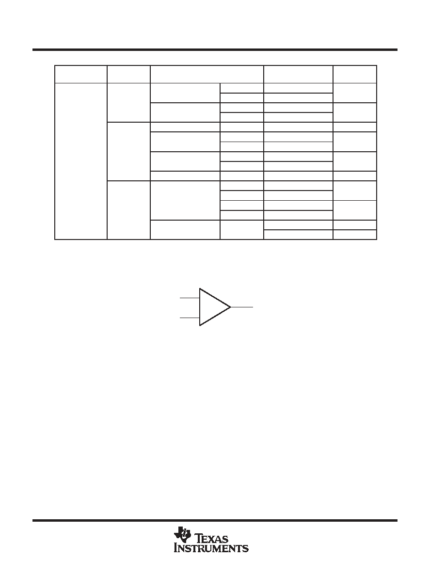
ORDERING INFORMATION
TA
PACKAGE
ORDERABLE
PART NUMBER
TOP-SIDE
MARKING
SC-70 (DCK)
Reel of 3000
LMV321IDCKR
R3_
Single
SC-70 (DCK)
Reel of 250
LMV321IDCKT
R3_
Single
SOT23-5 (DBV)
Reel of 3000
LMV321IDBVR
RC1_
SOT23-5 (DBV)
Reel of 250
LMV321IDBVT
RC1_
MSOP/VSSOP (DGK)
Reel of 2500
LMV358IDGKR
R5R
SOIC (D)
Tube of 75
LMV358ID
MV358I
Dual
SOIC (D)
Reel of 2500
LMV358IDR
MV358I
-40
∞
C to 85
∞
C
Dual
TSSOP (PW)
Tube of 150
LMV358IPW
MV358I
-40
∞
C to 85
∞
C
TSSOP (PW)
Reel of 2000
LMV358IPWR
MV358I
VSSOP (DDU)
Reel of 3000
LMV358IDDUR
RA56
Tube of 50
LMV324ID
LMV324I
SOIC (D)
Reel of 2500
LMV324IDR
LMV324I
Quad
SOIC (D)
Tube of 40
LMV324SID
LMV324SI
Quad
Reel of 2500
LMV324SIDR
LMV324SI
TSSOP (PW)
Reel of 2000
LMV324IPWR
MV324I
TSSOP (PW)
Reel of 2000
LMV324SIPWR
MV324SI
Package drawings, standard packing quantities, thermal data, symbolization, and PCB design guidelines are available at
www.ti.com/sc/package.
DBV/DCK: The actual top-side marking has one additional character that designates the assembly/test site.
symbol (each amplifier)
+
-
IN-
IN+
OUT

LMV321 SINGLE, LMV358 DUAL, LMV324 QUAD, LMV324S QUAD WITH SHUTDOWN
LOW VOLTAGE RAIL TO RAIL OUTPUT OPERATIONAL AMPLIFIERS
SLOS263M - AUGUST 1999 - REVISED OCTOBER 2003
3
POST OFFICE BOX 655303
∑
DALLAS, TEXAS 75265
absolute maximum ratings over operating free-air temperature range (unless otherwise noted)
Supply voltage, V
CC
(see Note 1)
5.5 V
. . . . . . . . . . . . . . . . . . . . . . . . . . . . . . . . . . . . . . . . . . . . . . . . . . . . . . . . . . .
Differential input voltage, V
ID
(see Note 2)
±
5.5 V
. . . . . . . . . . . . . . . . . . . . . . . . . . . . . . . . . . . . . . . . . . . . . . . . . .
Input voltage, V
I
(either input)
0 to 5.5 V
. . . . . . . . . . . . . . . . . . . . . . . . . . . . . . . . . . . . . . . . . . . . . . . . . . . . . . . . . .
Duration of output short circuit (one amplifier) to ground at (or below) T
A
=
25
∞
C,
V
CC
5.5 V (see Note 3)
Unlimited
. . . . . . . . . . . . . . . . . . . . . . . . . . . . . . . . . . . . . . . . . . . . . . . . . . . . . . . . . . . . .
Package thermal impedance,
JA
(see Notes 4 and 5): D (8-pin) package
97
∞
C/W
. . . . . . . . . . . . . . . . . . . . . .
D (14-pin) package
86
∞
C/W
. . . . . . . . . . . . . . . . . . . .
D (16-pin) package
73
∞
C/W
. . . . . . . . . . . . . . . . . . . .
DBV package
206
∞
C/W
. . . . . . . . . . . . . . . . . . . . . . . .
DCK package
252
∞
C/W
. . . . . . . . . . . . . . . . . . . . . . . .
DDU package
TBD
∞
C/W
. . . . . . . . . . . . . . . . . . . . . . .
DGK package
172
∞
C/W
. . . . . . . . . . . . . . . . . . . . . . . .
PW (8-pin) package
149
∞
C/W
. . . . . . . . . . . . . . . . . . .
PW (14-pin) package
113
∞
C/W
. . . . . . . . . . . . . . . . . .
PW (16-pin) package
108
∞
C/W
. . . . . . . . . . . . . . . . . .
Operating virtual junction temperature, T
J
150
∞
C
. . . . . . . . . . . . . . . . . . . . . . . . . . . . . . . . . . . . . . . . . . . . . . . . . . .
Storage temperature range, T
stg
-65
∞
C to 150
∞
C
. . . . . . . . . . . . . . . . . . . . . . . . . . . . . . . . . . . . . . . . . . . . . . . . . . .
Stresses beyond those listed under "absolute maximum ratings" may cause permanent damage to the device. These are stress ratings only, and
functional operation of the device at these or any other conditions beyond those indicated under "recommended operating conditions" is not
implied. Exposure to absolute-maximum-rated conditions for extended periods may affect device reliability.
NOTES:
1. All voltage values (except differential voltages and VCC specified for the measurement of IOS) are with respect to the network GND.
2. Differential voltages are at IN+ with respect to IN-.
3. Short circuits from outputs to VCC can cause excessive heating and eventual destruction.
4. Maximum power dissipation is a function of TJ(max),
JA, and TA. The maximum allowable power dissipation at any allowable
ambient temperature is PD = (TJ(max) - TA)/
JA. Selecting the maximum of 150
∞
C can affect reliability.
5. The package thermal impedance is calculated in accordance with JESD 51-7.
recommended operating conditions (see Note 6)
MIN
MAX
UNIT
VCC
Supply voltage (single-supply operation)
2.7
5.5
V
VIH
Amplifier turnon voltage level (LMV324S)
VCC = 2.7 V
1.7
V
VIH
Amplifier turnon voltage level (LMV324S)
VCC = 5 V
3.5
V
VIL
Amplifier turnoff voltage level (LMV324S)
VCC = 2.7 V
0.7
V
VIL
Amplifier turnoff voltage level (LMV324S)
VCC = 5 V
1.5
V
TA
Operating free-air temperature
-40
85
∞
C
VIH should not be allowed to exceed VCC.
NOTE 6: All unused control inputs of the device must be held at VCC or GND to ensure proper device operation. Refer to the TI application report,
Implications of Slow or Floating CMOS Inputs, literature number SCBA004.

LMV321 SINGLE, LMV358 DUAL, LMV324 QUAD, LMV324S QUAD WITH SHUTDOWN
LOW VOLTAGE RAIL TO RAIL OUTPUT OPERATIONAL AMPLIFIERS
SLOS263M - AUGUST 1999 - REVISED OCTOBER 2003
4
POST OFFICE BOX 655303
∑
DALLAS, TEXAS 75265
electrical characteristics at T
A
= 25
∞
C and V
CC+
= 2.7 V (unless otherwise noted)
PARAMETER
TEST CONDITIONS
MIN
TYP
MAX
UNIT
VIO
Input offset voltage
1.7
7
mV
a
V
IO
Average temperature coefficient
of input offset voltage
5
m
V/
∞
C
IIB
Input bias current
11
250
nA
IIO
Input offset current
5
50
nA
CMRR
Common-mode rejection ratio
VCM = 0 to 1.7 V
50
63
dB
kSVR
Supply-voltage rejection ratio
VCC = 2.7 V to 5 V,
VO = 1 V
50
60
dB
VICR
Common-mode input voltage range
CMRR
w
50 dB
0 to 1.7
-0.2 to 1.9
V
Output swing
RL = 10 k
to 1.35 V
High level
VCC-100
VCC-10
mV
Output swing
RL = 10 k
to 1.35 V
Low level
60
180
mV
LMV321I
80
170
ICC
Supply current
LMV358I (both amplifiers)
140
340
m
A
ICC
Supply current
LMV324I/LMV324SI (all four amplifiers)
260
680
m
A
B1
Unity-gain bandwidth
CL = 200 pF
1
MHz
F
m
Phase margin
60
deg
Gm
Gain margin
10
dB
Vn
Equivalent input noise voltage
f = 1 kHz
46
nV/
Hz
In
Equivalent input noise current
f = 1 kHz
0.17
pA/
Hz
shutdown characteristics (LMV324S) at T
A
= 25
∞
C and V
CC+
= 2.7 V (unless otherwise noted)
PARAMETER
TEST CONDITIONS
MIN
TYP
MAX
UNIT
ICC(SHDN)
Supply current in shutdown mode
(per channel)
SHDN
0.6 V
5
m
A
t(on)
Amplifier turnon time
AV = 1, RL = Open (measured at 50% point)
2
m
s
t(off)
Amplifier turnoff time
AV = 1, RL = Open (measured at 50% point)
40
ns

LMV321 SINGLE, LMV358 DUAL, LMV324 QUAD, LMV324S QUAD WITH SHUTDOWN
LOW VOLTAGE RAIL TO RAIL OUTPUT OPERATIONAL AMPLIFIERS
SLOS263M - AUGUST 1999 - REVISED OCTOBER 2003
5
POST OFFICE BOX 655303
∑
DALLAS, TEXAS 75265
electrical characteristics at specified free-air temperature range, V
CC+
= 5 V (unless otherwise
noted)
PARAMETER
TEST CONDITIONS
TA
MIN
TYP
MAX
UNIT
VIO
Input offset voltage
25
∞
C
1.7
7
mV
VIO
Input offset voltage
-40
∞
C to 85
∞
C
9
mV
a
V
IO
Average temperature coefficient
of input offset voltage
25
∞
C
5
m
V/
∞
C
IIB
Input bias current
25
∞
C
15
250
nA
IIB
Input bias current
-40
∞
C to 85
∞
C
500
nA
IIO
Input offset current
25
∞
C
5
50
nA
IIO
Input offset current
-40
∞
C to 85
∞
C
150
nA
CMRR
Common-mode rejection ratio
VCM = 0 to 4 V
25
∞
C
50
65
dB
kSVR
Supply-voltage rejection ratio
VCC= 2.7 V to 5 V, VO = 1 V,
VCM = 1 V
25
∞
C
50
60
dB
VICR
Common-mode
CMMR
w
50 dB
25
∞
C
0 to 4
-0.2 to 4.2
V
VICR
Common-mode
input voltage range
CMMR
w
50 dB
25
∞
C
0 to 4
-0.2 to 4.2
V
High level
25
∞
C
VCC-300
VCC-40
RL = 2 k
to 2.5 V
High level
-40
∞
C to 85
∞
C
VCC-400
RL = 2 k
to 2.5 V
Low level
25
∞
C
120
300
Output swing
Low level
-40
∞
C to 85
∞
C
400
mV
Output swing
High level
25
∞
C
VCC-100
VCC-10
mV
RL = 10 k
to 2.5 V
High level
-40
∞
C to 85
∞
C
VCC-200
RL = 10 k
to 2.5 V
Low level
25
∞
C
65
180
Low level
-40
∞
C to 85
∞
C
280
AVD
Large-signal differential
RL = 2 k
25
∞
C
15
100
V/mV
AVD
Large-signal differential
voltage gain
RL = 2 k
-40
∞
C to 85
∞
C
10
V/mV
IOS
Output short-circuit current
Sourcing, VO = 0 V
25
∞
C
5
60
mA
IOS
Output short-circuit current
Sinking, VO = 5 V
25
∞
C
10
160
mA
LMV321I
25
∞
C
130
250
LMV321I
-40
∞
C to 85
∞
C
350
ICC
Supply current
LMV358I (both amplifiers)
25
∞
C
210
440
A
ICC
Supply current
LMV358I (both amplifiers)
-40
∞
C to 85
∞
C
615
m
A
LMV324I/LMV324SI
25
∞
C
410
830
LMV324I/LMV324SI
(all four amplifiers)
-40
∞
C to 85
∞
C
1160
B1
Unity-gain bandwidth
CL = 200 pF
25
∞
C
1
MHz
f
m
Phase margin
25
∞
C
60
deg
Gm
Gain margin
25
∞
C
10
dB
Vn
Equivalent input noise voltage
f = 1 kHz
25
∞
C
39
nV/
Hz
In
Equivalent input noise current
f = 1 kHz
25
∞
C
0.21
pA/
Hz
SR
Slew rate
25
∞
C
1
V/
m
s
shutdown characteristics (LMV324S) at T
A
= 25
∞
C and V
CC+
= 5 V (unless otherwise noted)
PARAMETER
TEST CONDITIONS
TA
MIN
TYP
MAX
UNIT
ICC(SHDN)
Supply current in shutdown mode
(per channel)
SHDN
0.6 V
-40
∞
C to 85
∞
C
5
m
A
t(on)
Amplifier turnon time
AV = 1, RL = Open (measured at 50% point)
2
m
s
t(off)
Amplifier turnoff time
AV = 1, RL = Open (measured at 50% point)
40
ns