
µ
A78L00 SERIES
POSITIVE-VOLTAGE REGULATORS
SLVS010I ≠ JANUARY 1976 ≠ REVISED JULY 1999
1
POST OFFICE BOX 655303
∑
DALLAS, TEXAS 75265
D
3-Terminal Regulators
D
Output Current up to 100 mA
D
No External Components
D
Internal Thermal-Overload Protection
D
Internal Short-Circuit Current Limiting
D
Direct Replacements for Fairchild
µ
A78L00
Series
description
This series of fixed-voltage integrated-circuit
voltage regulators is designed for a wide range of
applications. These applications include on-card
regulation for elimination of noise and distribution
problems associated with single-point regulation.
In addition, they can be used with power-pass
elements to make high-current voltage regulators.
One of these regulators can deliver up to 100 mA
of output current. The internal limiting and
thermal-shutdown features of these regulators
make them essentially immune to overload. When
used as a replacement for a zener diode-resistor
combination, an effective improvement in output
impedance can be obtained, together with lower
bias current.
The
µ
A78L00C series is characterized for
operation over the virtual junction temperature
range of 0
∞
C to 125
∞
C.
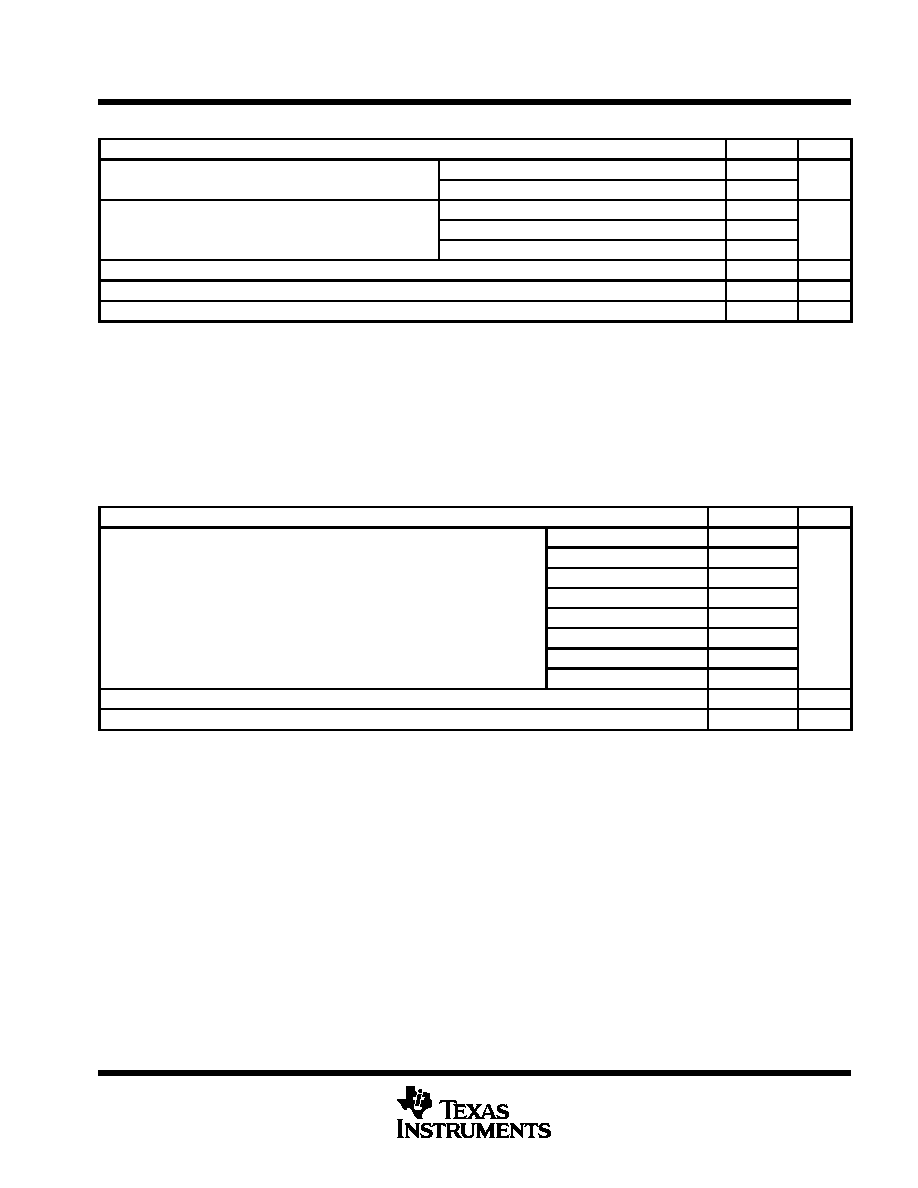
AVAILABLE OPTIONS
PACKAGED DEVICES
TJ
VO(NOM)
(V)
SMALL OUTLINE
(D)
PLASTIC CYLINDRICAL
(LP)
SOT-89
(PK)
CHIP
FORM
J
(V)
OUTPUT VOLTAGE TOLERANCE
(Y)
5%
10%
5%
10%
5%
10%
0
∞
C to
125
∞
C
2.6
5
6.2
8
9
10
12
15
µ
A78L02ACD
µ
A78L05ACD
µ
A78L06ACD
µ
A78L08ACD
µ
A78L09ACD
µ
A78L10ACD
µ
A78L12ACD
µ
A78L15ACD
≠
µ
A78L05CD
µ
A78L06CD
µ
A78L08CD
µ
A78L09CD
≠
µ
A78L12CD
µ
A78L15CD
µ
A78L02ACLP
µ
A78L05ACLP
µ
A78L06ACLP
µ
A78L08ACLP
µ
A78L09ACLP
µ
A78L10ACLP
µ
A78L12ACLP
µ
A78L15ACLP
µ
A78L02CLP
µ
A78L05CLP
µ
A78L06CLP
µ
A78L08CLP
µ
A78L09CLP
µ
A78L10CLP
µ
A78L12CLP
µ
A78L15CLP
µ
A78L02ACPK
µ
A78L05ACPK
µ
A78L06ACPK
µ
A78L08ACPK
µ
A78L09ACPK
µ
A78L10ACPK
µ
A78L12ACPK
µ
A78L15ACPK
µ
A78L02CPK
µ
A78L05CPK
µ
A78L06CPK
µ
A78L08CPK
µ
A78L09CPK
µ
A78L10CPK
µ
A78L12CPK
µ
A78L15CPK
µ
A78L02Y
µ
A78L05Y
µ
A78L06Y
µ
A78L08Y
µ
A78L09Y
µ
A78L10Y
µ
A78L12Y
µ
A78L15Y
D and LP packages are available taped and reeled. Add the suffix R to the device type (e.g.,
µ
A78L05ACDR). The PK package is only available
taped and reeled (e.g.,
µ
A78L02ACPKR). Chip forms are tested at TA = 25
∞
C.
Please be aware that an important notice concerning availability, standard warranty, and use in critical applications of
Texas Instruments semiconductor products and disclaimers thereto appears at the end of this data sheet.
Copyright
©
1999, Texas Instruments Incorporated
PRODUCTION DATA information is current as of publication date.
Products conform to specifications per the terms of Texas Instruments
standard warranty. Production processing does not necessarily include
testing of all parameters.
D PACKAGE
(TOP VIEW)
1
2
3
4
8
7
6
5
OUTPUT
COMMON
COMMON
NC
INPUT
COMMON
COMMON
NC
LP PACKAGE
(TOP VIEW)
PK PACKAGE
(TOP VIEW)
NC ≠ No internal connection
INPUT
COMMON
OUTPUT
INPUT
COMMON
OUTPUT
TO≠226AA

µ
A78L00 SERIES
POSITIVE-VOLTAGE REGULATORS
SLVS010I ≠ JANUARY 1976 ≠ REVISED JULY 1999
2
POST OFFICE BOX 655303
∑
DALLAS, TEXAS 75265
schematic
20 k
1 k
to 14 k
INPUT
OUTPUT
COMMON
NOTE: Resistor values shown are nominal.
1.4 k
µ
A78L00 SERIES
POSITIVE-VOLTAGE REGULATORS
SLVS010I ≠ JANUARY 1976 ≠ REVISED JULY 1999
3
POST OFFICE BOX 655303
∑
DALLAS, TEXAS 75265
absolute maximum ratings over operating temperature range (unless otherwise noted)
µ
A78Lxx
UNIT
Input voltage VI
µ
A78L02AC,
µ
A78L05C≠
µ
A78L09C,
µ
A78L10AC
30
V
Input voltage, VI
µ
A78L12C,
µ
A78L12AC,
µ
A78L15C,
µ
A78L15AC
35
V
D package
97
Package thermal impedance,
JA (see Notes 1 and 2)
LP package
156
∞
C
PK package
52
Virtual junction temperature range, TJ
0 to 150
∞
C
Lead temperature 1,6 mm (1/16 inch) from case for 10 seconds
260
∞
C
Storage temperature range, Tstg
≠65 to 150
∞
C
Stresses beyond those listed under "absolute maximum ratings" may cause permanent damage to the device. These are stress ratings only, and
functional operation of the device at these or any other conditions beyond those indicated under "recommended operating conditions" is not
implied. Exposure to absolute-maximum-rated conditions for extended periods may affect device reliability.
NOTES:
1. Maximum power dissipation is a function of TJ(max),
JA, and TA. The maximum allowable power dissipation at any allowable
ambient temperature is PD = (TJ(max) ≠ TA)/
JA. Operating at the absolute maximum TJ of 150
∞
C can impact reliability. Due to
variations in individual device electrical characteristics and thermal resistance, the built-in thermal-overload protection may be
activated at power levels slightly above or below the rated dissipation.
2. The package thermal impedance is calculated in accordance with JESD 51, except for through-hole packages, which use a trace
length of zero.
recommended operating conditions
MIN
MAX
UNIT
µ
A78L02AC
4.75
20
µ
A78L05C,
µ
A78L05AC
7
20
µ
A78L06C,
µ
A78L06AC
8.5
20
Input voltage VI
µ
A78L08C,
µ
A78L08AC
10.5
23
V
Input voltage, VI
µ
A78L09C,
µ
A78L09AC
11.5
24
V
µ
A78L10AC
12.5
25
µ
A78L12C,
µ
A78L12AC
14.5
27
µ
A78L15C,
µ
A78L15AC
17.5
30
Output current, IO
100
mA
Operating virtual junction temperature, TJ
0
125
∞
C

µ
A78L00 SERIES
POSITIVE-VOLTAGE REGULATORS
SLVS010I ≠ JANUARY 1976 ≠ REVISED JULY 1999
4
POST OFFICE BOX 655303
∑
DALLAS, TEXAS 75265
electrical characteristics at specified virtual junction temperature, V
I
= 9 V, I
O
= 40 mA (unless
otherwise noted)
PARAMETER
TEST CONDITIONS
T
µ
A78L02C
UNIT
PARAMETER
TEST CONDITIONS
TJ
MIN
TYP
MAX
UNIT
V
4 75 V to 20 V
I
1 mA to 40 mA
25
∞
C
2.5
2.6
2.7
Output voltage
VI = 4.75 V to 20 V,
IO = 1 mA to 40 mA
0
∞
C to 125
∞
C
2.45
2.75
V
IO = 1 mA to 70 mA
0
∞
C to 125
∞
C
2.45
2.75
Input voltage regulation
VI = 4.75 V to 20 V
25
∞
C
20
100
mV
Input voltage regulation
VI = 5 V to 20 V
25
∞
C
16
75
mV
Ripple rejection
VI = 6 V to 20 V,
f = 120 Hz
25
∞
C
43
51
dB
Output voltage regulation
IO = 1 mA to 100 mA
25
∞
C
12
50
mV
Output voltage regulation
IO = 1 mA to 40 mA
25
∞
C
6
25
mV
Output noise voltage
f = 10 Hz to 100 kHz
25
∞
C
30
µ
V
Dropout voltage
25
∞
C
1.7
V
Bias current
25
∞
C
3.6
6
mA
Bias current
125
∞
C
5.5
mA
Bias current change
VI = 5 V to 20 V
0
∞
C to 125
∞
C
2.5
mA
Bias current change
IO = 1 mA to 40 mA
0
∞
C to 125
∞
C
0.1
mA
Pulse-testing techniques maintain TJ as close to TA as possible. Thermal effects must be taken into account separately. All characteristics are
measured with a 0.33-
µ
F capacitor across the input and a 0.1-
µ
F capacitor across the output.
electrical characteristics at specified virtual junction temperature, V
I
= 10 V, I
O
= 40 mA (unless
otherwise noted)
PARAMETER
TEST CONDITIONS
TJ
µ
A78L05C
µ
A78L05AC
UNIT
PARAMETER
TEST CONDITIONS
TJ
MIN
TYP
MAX
MIN
TYP
MAX
UNIT
V
7 V to 20 V
I
1 mA to 40 mA
25
∞
C
4.6
5
5.4
4.8
5
5.2
Output voltage
VI = 7 V to 20 V,
IO = 1 mA to 40 mA
0
∞
C to 125
∞
C
4.5
5.5
4.75
5.25
V
IO = 1 mA to 70 mA
0
∞
C to 125
∞
C
4.5
5.5
4.75
5.25
Input
VI = 7 V to 20 V
25
∞
C
32
200
32
150
mV
voltage regulation
VI = 8 V to 20 V
25
∞
C
26
150
26
100
mV
Ripple rejection
VI = 8 V to 18 V,
f = 120 Hz
25
∞
C
40
49
41
49
dB
Output
IO = 1 mA to 100 mA
25
∞
C
15
60
15
60
mV
voltage regulation
IO = 1 mA to 40 mA
25
∞
C
8
30
8
30
mV
Output
noise voltage
f = 10 Hz to 100 kHz
25
∞
C
42
42
µ
V
Dropout voltage
25
∞
C
1.7
1.7
V
Bias current
25
∞
C
3.8
6
3.8
6
mA
Bias current
125
∞
C
5.5
5.5
mA
Bias
VI = 8 V to 20 V
0
∞
C to 125
∞
C
1.5
1.5
mA
current change
IO = 1 mA to 40 mA
0
∞
C to 125
∞
C
0.2
0.1
mA
Pulse-testing techniques maintain TJ as close to TA as possible. Thermal effects must be taken into account separately. All characteristics are
measured with a 0.33-
µ
F capacitor across the input and a 0.1-
µ
F capacitor across the output.

µ
A78L00 SERIES
POSITIVE-VOLTAGE REGULATORS
SLVS010I ≠ JANUARY 1976 ≠ REVISED JULY 1999
5
POST OFFICE BOX 655303
∑
DALLAS, TEXAS 75265
electrical characteristics at specified virtual junction temperature, V
I
= 12 V, I
O
= 40 mA (unless
otherwise noted)
PARAMETER
TEST CONDITIONS
TJ
µ
A78L06C
µ
A78L06AC
UNIT
PARAMETER
TEST CONDITIONS
TJ
MIN
TYP
MAX
MIN
TYP
MAX
UNIT
V
8 5 V to 20 V
I
1 mA to 40 mA
25
∞
C
5.7
6.2
6.7
5.95
6.2
6.45
Output voltage
VI = 8.5 V to 20 V,
IO = 1 mA to 40 mA
0
∞
C to 125
∞
C
5.6
6.8
5.9
6.5
V
IO = 1 mA to 70 mA
0
∞
C to 125
∞
C
5.6
6.8
5.9
6.5
Input
VI = 8.5 V to 20 V
25
∞
C
35
200
35
175
mV
voltage regulation
VI = 9 V to 20 V
25
∞
C
29
150
29
125
mV
Ripple rejection
VI = 10 V to 20 V,
f = 120 Hz
25
∞
C
39
48
40
48
dB
Output
IO = 1 mA to 100 mA
25
∞
C
16
80
16
80
mV
voltage regulation
IO = 1 mA to 40 mA
25
∞
C
9
40
9
40
mV
Output
noise voltage
f = 10 Hz to 100 kHz
25
∞
C
46
46
µ
V
Dropout voltage
25
∞
C
1.7
1.7
V
Bias current
25
∞
C
3.9
6
3.9
6
mA
Bias current
125
∞
C
5.5
5.5
mA
Bias
VI = 9 V to 20 V
0
∞
C to 125
∞
C
1.5
1.5
mA
current change
IO = 1 mA to 40 mA
0
∞
C to 125
∞
C
0.2
0.1
mA
Pulse-testing techniques maintain TJ as close to TA as possible. Thermal effects must be taken into account separately. All characteristics are
measured with a 0.33-
µ
F capacitor across the input and a 0.1-
µ
F capacitor across the output.
electrical characteristics at specified virtual junction temperature, V
I
= 14 V, I
O
= 40 mA (unless
otherwise noted)
PARAMETER
TEST CONDITIONS
TJ
µ
A78L08C
µ
A78L08AC
UNIT
PARAMETER
TEST CONDITIONS
TJ
MIN
TYP
MAX
MIN
TYP
MAX
UNIT
V
10 5 V to 23 V
I
1 mA to 40 mA
25
∞
C
7.36
8
8.64
7.7
8
8.3
Output voltage
VI = 10.5 V to 23 V, IO = 1 mA to 40 mA
0
∞
C to 125
∞
C
7.2
8.8
7.6
8.4
V
IO = 1 mA to 70 mA
0
∞
C to 125
∞
C
7.2
8.8
7.6
8.4
Input voltage
VI = 10.5 V to 23 V
25
∞
C
42
200
42
175
mV
g
regulation
VI = 11 V to 23 V
25
∞
C
36
150
36
125
mV
Ripple rejection
VI = 13 V to 23 V,
f = 120 Hz
25
∞
C
36
46
37
46
dB
Output voltage
IO = 1 mA to 100 mA
25
∞
C
18
80
18
80
mV
g
regulation
IO = 1 mA to 40 mA
25
∞
C
10
40
10
40
mV
Output
noise voltage
f = 10 Hz to 100 kHz
25
∞
C
54
54
µ
V
Dropout voltage
25
∞
C
1.7
1.7
V
Bias current
25
∞
C
4
6
4
6
mA
Bias current
125
∞
C
5.5
5.5
mA
Bias
VI = 5 V to 20 V
0
∞
C to 125
∞
C
1.5
1.5
mA
current change
IO = 1 mA to 40 mA
0
∞
C to 125
∞
C
0.2
0.1
mA
Pulse-testing techniques maintain TJ as close to TA as possible. Thermal effects must be taken into account separately. All characteristics are
measured with a 0.33-
µ
F capacitor across the input and a 0.1-
µ
F capacitor across the output.