
1
2
3
4
8
7
6
5
V+
Out B
≠In B
+In B
Out A
≠In A
+In A
V≠
OPA2137
8-Pin DIP, SO-8, MSOP-8
A
B
1
2
3
4
8
7
6
5
NC
V+
Output
NC
NC
≠In
+In
V≠
OPA137
8-Pin DIP, SO-8
1
2
3
5
4
V+
≠In
Out
V≠
+In
OPA137
SOT-23-5
LOW COST
FET-INPUT OPERATIONAL AMPLIFIERS
Micro
Amplifier
TM
Series
International Airport Industrial Park ∑ Mailing Address: PO Box 11400, Tucson, AZ 85734 ∑ Street Address: 6730 S. Tucson Blvd., Tucson, AZ 85706 ∑ Tel: (520) 746-1111 ∑ Twx: 910-952-1111
Internet: http://www.burr-brown.com/ ∑ FAXLine: (800) 548-6133 (US/Canada Only) ∑ Cable: BBRCORP ∑ Telex: 066-6491 ∑ FAX: (520) 889-1510 ∑ Immediate Product Info: (800) 548-6132
© 1998 Burr-Brown Corporation
PDS-1438A
Printed in U.S.A. August, 1998
OPA137
OPA2137
OPA4137
Æ
FEATURES
q
FET INPUT: I
B
= 5pA
q
LOW OFFSET VOLTAGE: 1.5mV
q
WIDE SUPPLY RANGE:
±
2.25V to
±
18V
q
LOW QUIESCENT CURRENT: 220
µ
A/channel
q
EXCELLENT SPEED/POWER: 1MHz
q
INPUT TO POSITIVE SUPPLY
q
Micro
SIZE PACKAGES: SOT-23-5, MSOP-8
q
SINGLE, DUAL, AND QUAD
DESCRIPTION
OPA137 series FET-input operational amplifiers are designed
for low cost and miniature applications. In addition to small
size (SOT-23-5 and MSOP-8 packages), they provide low
input bias current (5pA), low quiescent currrent (220
µ
A/
channel), and high open-loop gain (94dB).
Either single (+4.5V to +36V) or dual (
±
2.25 to
±
18V)
supplies can be used. The input common-mode voltage range
includes the positive supply--suitable for many single-supply
applications. Single, dual, and quad versions have identical
specifications for maximum design flexibility.
OPA137 op amps are easy to use and free from phase
inversion and overload problems found in some FET-input
amplifiers. High performance, including linearity, is main-
tained as the amplifiers swing to their specified limits. In
addition, the combination of high slew rate (3.5V/
µ
s) and
wide bandwidth (1MHz) provide fast settling time assuring
good dynamic response. Dual and quad designs feature com-
pletely independent circuitry for lowest crosstalk and freedom
from interaction.
The single (OPA137) packages are the tiny 5-lead SOT-23-5
surface mount, SO-8 surface mount, and 8-pin DIP. The dual
(OPA2137) comes in the miniature MSOP-8 surface mount,
SO-8 surface mount, and 8-pin DIP packages. The quad
(OPA4137) packages are the SO-14 surface mount and the
14-pin DIP. All are specified from ≠40
∞
C to +85
∞
C and operate
from ≠55
∞
C to +125
∞
C. A SPICE macromodel is available for
design analysis.
APPLICATIONS
q
STRAIN GAGE AMPLIFIER
q
PHOTODETECTOR AMPLIFIER
q
PRECISION INTEGRATOR
q
BATTERY-POWERED INSTRUMENTS
q
TEST EQUIPMENT
q
ACTIVE FILTERS
1
2
3
4
5
6
7
14
13
12
11
10
9
8
Out D
≠In D
+In D
V≠
+In C
≠In C
Out C
Out A
≠In A
+In A
V+
+In B
≠In B
Out B
OPA4137
14-Pin DIP
SO-14
A
D
B
C
OPA4137
OPA137
OPA2137
OPA4137
SBOS089

2
Æ
OPA137, 2137, 4137
SPECIFICATIONS: V
S
=
±
15V
At T
A
= +25
∞
C, R
L
= 10k
connected to ground, unless otherwise noted.
Boldface limits apply over the specified temperature range, T
A
= ≠40
∞
C to +85
∞
C.
OPA137N, U, P
OPA137NA, UA, PA
OPA2137E, U, P
OPA2137EA, UA, PA
OPA4137U, P
OPA4137UA, PA
PARAMETER
CONDITION
MIN
TYP
MAX
MIN
TYP
MAX
UNITS
OFFSET VOLTAGE
Input Offset Voltage
V
OS
±
1.5
±
3
±
2.5
±
10
mV
T
A
= ≠40
∞
C to +85
∞
C
±
2.5
±
7
±
3.5
±
15
mV
vs Temperature
dV
OS
/dT
T
A
= ≠40
∞
C to +85
∞
C
±
15
T
µ
V/
∞
C
vs Power Supply
PSRR
V
S
=
±
3V to
±
18V
±
90
±
250
T
T
µ
V/V
T
A
= ≠40
∞
C to +85
∞
C
±
250
T
µ
V/V
Channel Separation (dual, quad)
dc
0.6
T
µ
V/V
INPUT BIAS CURRENT
V
CM
= 0V
Input Bias Current
I
B
±
5
±
100
T
T
pA
vs Temperature
See Typical Curve
T
Input Offset Current
I
OS
±
2
±
50
T
T
pA
NOISE
Input Voltage Noise, f = 0.1 to 10Hz
2
T
µ
Vp-p
Input Voltage Noise Density, f = 1kHz
e
n
45
T
nV/
Hz
Current Noise Density, f = 1kHz
i
n
1.2
T
fA/
Hz
INPUT VOLTAGE RANGE
Common-Mode Voltage Range
V
CM
(V≠) + 3
(V+)
T
T
V
Common-Mode Rejection Ratio
CMRR
V
CM
= ≠12V to 15V
OPA137, OPA2137
76
84
70
T
dB
OPA4137
74
84
70
T
dB
T
A
= ≠40
∞
C to +85
∞
C
V
CM
= ≠12V to 15V
OPA137, OPA2137
72
70
dB
OPA4137
70
70
dB
INPUT IMPEDANCE
Differential
10
10
|| 1
T
|| pF
Common-Mode
10
12
|| 2
T
|| pF
OPEN-LOOP GAIN
Open-Loop Voltage Gain
A
OL
V
O
= ≠13.8V to 13.9V
86
94
T
T
dB
T
A
= ≠40
∞
C to +85
∞
C
V
O
= ≠13.8V to 13.9V
86
T
dB
FREQUENCY RESPONSE
Gain-Bandwidth Product
GBW
1
T
MHz
Slew Rate
SR
G = 1
3.5
T
V/
µ
s
Settling Time, 0.1%
G = 1, 10V Step, C
L
= 100pF
8
T
µ
s
0.01%
G = 1, 10V Step, C
L
= 100pF
10
T
µ
s
Overload Recovery Time
V
IN
∑ G = V
S
1
T
µ
s
Total Harmonic Distortion + Noise
THD+N
G = 1, f = 1kHz, 3.5Vrms
0.05
T
%
OUTPUT
Voltage Output
V
OUT
(V≠) + 1.2
(V+) ≠ 1.1
T
T
V
T
A
= ≠40
∞
C to +85
∞
C
(V≠) + 1.2
(V+) ≠ 1.1
T
T
V
Short-Circuit Current
I
SC
≠25/+60
T
mA
Capacitive Load Drive
C
LOAD
1000
T
pF
POWER SUPPLY
Specified Operating Range
V
S
±
15
T
V
Operating Voltage Range
Dual Supplies
±
2.25
(1)
±
18
T
T
V
Single Supply
+4.5
+36
T
T
V
Quiescent Current
I
Q
I
O
= 0
±
220
±
270
T
T
µ
A
T
A
= ≠40
∞
C to +85
∞
C
I
O
= 0
±
375
T
µ
A
TEMPERATURE RANGE
Specified Range
≠40
+85
T
T
∞
C
Operating Range
≠55
+125
T
T
∞
C
Storage Range
≠55
+125
T
T
∞
C
Thermal Resistance
JA
SOT-23-5 Surface Mount
200
T
∞
C/W
MSOP-8 Surface Mount
150
T
∞
C/W
SO-8 Surface Mount
150
T
∞
C/W
8-Pin DIP
100
T
∞
C/W
SO-14 Surface Mount
100
T
∞
C/W
14-Pin DIP
80
T
∞
C/W
T
Specifications the same as OPA137N, U, P.
NOTE: (1) At minimum power supply voltage inputs must be biased above ground in accordance with common-mode voltage range restrictions--see "Operating
Voltage" discussion.

3
Æ
OPA137, 2137, 4137
ELECTROSTATIC
DISCHARGE SENSITIVITY
This integrated circuit can be damaged by ESD. Burr-Brown
recommends that all integrated circuits be handled with
appropriate precautions. Failure to observe proper handling
and installation procedures can cause damage.
ESD damage can range from subtle performance degrada-
tion to complete device failure. Precision integrated circuits
may be more susceptible to damage because very small
parametric changes could cause the device not to meet its
published specifications.
Supply Voltage, V+ to V≠ ..................................................................... 36V
Input Voltage ....................................................... (V≠) ≠0.7V to (V+) +0.7V
Input Current ....................................................................................... 2mA
Output Short-Circuit
(2)
.............................................................. Continuous
Operating Temperature .................................................. ≠55
∞
C to +125
∞
C
Storage Temperature ...................................................... ≠55
∞
C to +125
∞
C
Junction Temperature .................................................................... +150
∞
C
Lead Temperature (soldering, 10s) ................................................. 300
∞
C
NOTE: (1) Stresses above these ratings may cause permanent damage.
Exposure to absolute maximum ratings for extended periods may affact device
reliability. (2) Short circuit to ground, one amplifier per package.
ABSOLUTE MAXIMUM RATINGS
(1)
PACKAGE
SPECIFIED
DRAWING
TEMPERATURE
PACKAGE
ORDERING
TRANSPORT
PRODUCT
PACKAGE
NUMBER
(1)
RANGE
MARKING
NUMBER
(2)
MEDIA
Single
OPA137N
5-Lead SOT-23-5 Surface Mount
331
≠40
∞
C to +85
∞
C
E37
(3)
OPA137N/250
Tape and Reel
"
"
"
"
"
OPA137N/3K
Tape and Reel
OPA137NA
5-Lead SOT-23-5 Surface Mount
331
≠40
∞
C to +85
∞
C
E37
(3)
OPA137NA/250
Tape and Reel
"
"
"
"
"
OPA137NA/3K
Tape and Reel
OPA137U
SO-8 Surface Mount
182
≠40
∞
C to +85
∞
C
OPA137U
OPA137U
Rails
"
"
"
"
"
OPA137U/2K5
Tape and Reel
OPA137UA
SO-8 Surface Mount
182
≠40
∞
C to +85
∞
C
OPA137UA
OPA137UA
Rails
"
"
"
"
"
OPA137UA/2K5
Tape and Reel
OPA137P
8-Pin DIP
006
≠40
∞
C to +85
∞
C
OPA137P
OPA137P
Rails
OPA137PA
8-Pin DIP
006
≠40
∞
C to +85
∞
C
OPA137PA
OPA137PA
Rails
Dual
OPA2137E
MSOP-8 Surface Mount
337
≠40
∞
C to +85
∞
C
E37
(3)
OPA2137E/250
Tape and Reel
"
"
"
"
"
OPA2137E/2K5
Tape and Reel
OPA2137EA
MSOP-8 Surface Mount
337
≠40
∞
C to +85
∞
C
E37
(3)
OPA2137EA/250
Tape and Reel
"
"
"
"
"
OPA2137EA/2K5
Tape and Reel
OPA2137U
SO-8 Surface Mount
182
≠40
∞
C to +85
∞
C
OPA2137U
OPA2137U
Rails
"
"
"
"
"
OPA2137U/2K5
Tape and Reel
OPA2137UA
SO-8 Surface Mount
182
≠40
∞
C to +85
∞
C
OPA2137UA
OPA2137UA
Rails
"
"
"
"
"
OPA2137UA/2K5
Tape and Reel
OPA2137P
8-Pin DIP
006
≠40
∞
C to +85
∞
C
OPA2137P
OPA2137P
Rails
OPA2137PA
8-Pin DIP
006
≠40
∞
C to +85
∞
C
OPA2137PA
OPA2137PA
Rails
Quad
OPA4137U
SO-14 Surface Mount
235
≠40
∞
C to +85
∞
C
OPA4137U
OPA4137U
Rails
"
"
"
"
"
OPA4137U/2K5
Tape and Reel
OPA4137UA
SO-14 Surface Mount
235
≠40
∞
C to +85
∞
C
OPA4137UA
OPA4137UA
Rails
"
"
"
"
"
OPA4137UA/2K5
Tape and Reel
OPA4137P
14-Pin DIP
010
≠40
∞
C to +85
∞
C
OPA4137P
OPA4137P
Rails
OPA4137PA
14-Pin DIP
010
≠40
∞
C to +85
∞
C
OPA4137PA
OPA4137PA
Rails
NOTES: (1) For detailed drawing and dimension table, please see end of data sheet, or Appendix C of Burr-Brown IC Data Book. (2) Models with a slash (/) are
available only in Tape and Reel in the quantities indicated (e.g., /2K5 indicates 2500 devices per reel). Ordering 3000 pieces of "OPA137NA/3K" will get a single
3000-piece Tape and Reel. For detailed Tape and Reel mechanical information, refer to Appendix B of Burr-Brown IC Data Book. (3) Grade information is marked
on the reel.
PACKAGE/ORDERING INFORMATION
The information provided herein is believed to be reliable; however, BURR-BROWN assumes no responsibility for inaccuracies or omissions. BURR-BROWN assumes no
responsibility for the use of this information, and all use of such information shall be entirely at the user's own risk. Prices and specifications are subject to change without notice.
No patent rights or licenses to any of the circuits described herein are implied or granted to any third party. BURR-BROWN does not authorize or warrant any BURR-BROWN product
for use in life support devices and/or systems.
4
Æ
OPA137, 2137, 4137
TYPICAL PERFORMANCE CURVES
At T
A
= +25
∞
C, V
S
=
±
15V, R
L
= 10k
, connected to ground, unless otherwise noted.
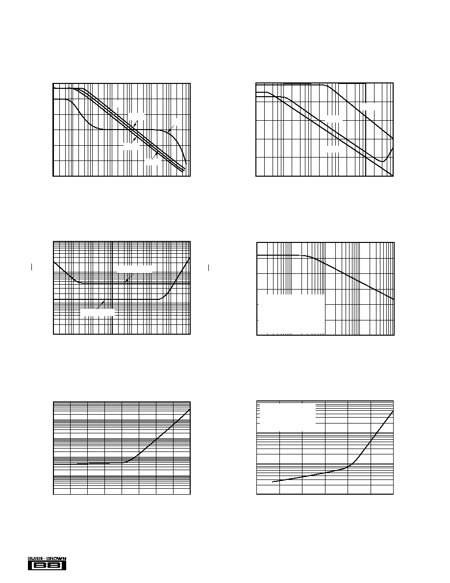
CHANNEL SEPARATION vs FREQUENCY
Frequency (Hz)
Channel Separation (dB)
140
120
100
80
60
40
20
100
1k
10k
100k
1M
Dual and quad devices.
G = 1, all channels.
Quad measured channel
A to D or B to C--other
combinations yield improved
rejection.
INPUT BIAS CURRENT
vs INPUT COMMON-MODE VOLTAGE
Common-Mode Voltage (V)
Input Bias Current (pA)
1n
100p
10p
1p
≠15
≠10
≠5
0
5
10
15
Input bias current is a
function of the voltage
between the V≠ supply
and the inputs.
INPUT VOLTAGE AND CURRENT NOISE
SPECTRAL DENSITY vs FREQUENCY
0.1
1k
100
10
1
1
10
1
0.1
Frequency (Hz)
1
10
100
1k
10k
100k
1M
Voltage Noise (nV/
Hz)
Current Noise (fA/
Hz)
Current Noise
Voltage Noise
POWER SUPPLY AND COMMON-MODE REJECTION
vs FREQUENCY
Frequency (Hz)
PSRR, CMRR (dB)
100
80
60
40
20
0
10
100
1k
10k
100k
1M
CMRR
≠PSRR
+PSRR
OPEN-LOOP GAIN/PHASE vs FREQUENCY
1
10
100
1k
10k
100k
1M
10M
100
80
60
40
20
0
≠20
0
≠45
≠90
≠135
≠180
Gain (dB)
Phase Shift (∞)
Frequency (Hz)
G
≠40∞C
+85∞C
+25∞C
INPUT BIAS CURRENT vs TEMPERATURE
Temperature (∞C)
Input Bias Current (pA)
10k
1k
100
10
1
0.1
≠75
≠50
≠25
0
25
50
75
100
125
5
Æ
OPA137, 2137, 4137
TYPICAL PERFORMANCE CURVES
(CONT)
At T
A
= +25
∞
C, V
S
=
±
15V, R
L
= 10k
, connected to ground, unless otherwise noted.
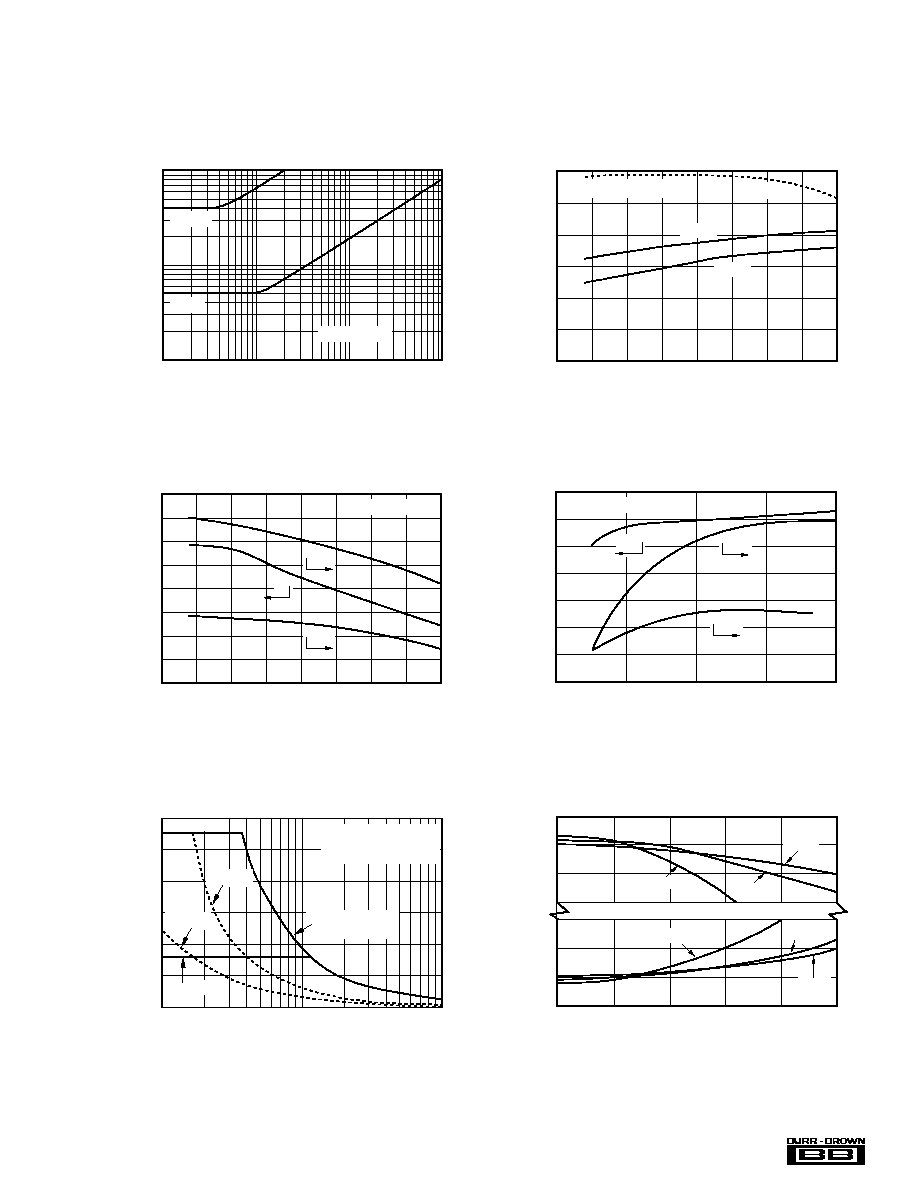
OUTPUT VOLTAGE SWING vs OUTPUT CURRENT
(V+)
(V+) ≠1
(V+) ≠2
(V+) ≠3
(V≠) +3
(V≠) +2
(V≠) +1
(V≠)
0
±2
±4
±6
±8
±10
Output Current (mA)
Output Voltage Swing (V)
≠55∞C
≠55∞C
+25∞C
+125∞C
+125∞C
+25∞C
QUIESCENT CURRENT and SHORT-CIRCUIT CURRENT
vs SUPPLY VOLTAGE
Supply Voltage (V)
Quiescent Current (µA)
Short-Circuit Current (mA)
±230
±220
±210
±200
±190
±180
±170
±160
±70
±60
±50
±40
±30
±20
±10
0
0
±5
±10
±15
±20
±I
SC
I
Q
≠I
SC
(I
Q
Per Amplifier)
TOTAL HARMONIC DISTORTION + NOISE
vs FREQUENCY
Frequency (Hz)
THD+N (%)
1
0.1
0.01
100k
100
1k
10k
G = 10
G = 1
V
O
= 3.5Vrms
A
OL
, CMRR, PSRR vs TEMPERATURE
Temperature (
∞
C)
A
OL
, CMRR, PSRR (dB)
95
90
85
80
75
70
65
≠75
≠50
≠25
0
25
50
75
100
125
PSRR
CMRR
V
O
= ≠13.8V to +13.9V
A
OL
QUIESCENT CURRENT and SHORT-CIRCUIT CURRENT
vs TEMPERATURE
Temperature (
∞
C)
Quiescent Current (
µ
A)
Short-Circuit Current (mA)
±
400
±
350
±
300
±
250
±
200
±
150
±
100
±
50
0
±
80
±
70
±
60
±
50
±
40
±
30
±
20
±
10
0
≠75
≠50
≠25
0
25
50
75
100
125
+I
SC
(I
Q
Per Amplifier)
I
Q
≠I
SC
MAXIMUM OUTPUT VOLTAGE vs FREQUENCY
Frequency (Hz)
10k
100k
1M
30
25
20
15
10
5
0
Output Voltage (Vp-p)
Without slew-rate
induced distortion
Maximum output voltage
without visible dynamic
distortion.
V
S
=
±
5V
C
L
= 200pF
V
S
=
±
15V
C
L
= 100pF
6
Æ
OPA137, 2137, 4137
TYPICAL PERFORMANCE CURVES
(CONT)
At T
A
= +25
∞
C, V
S
=
±
15V, R
L
= 10k
, connected to ground, unless otherwise noted.
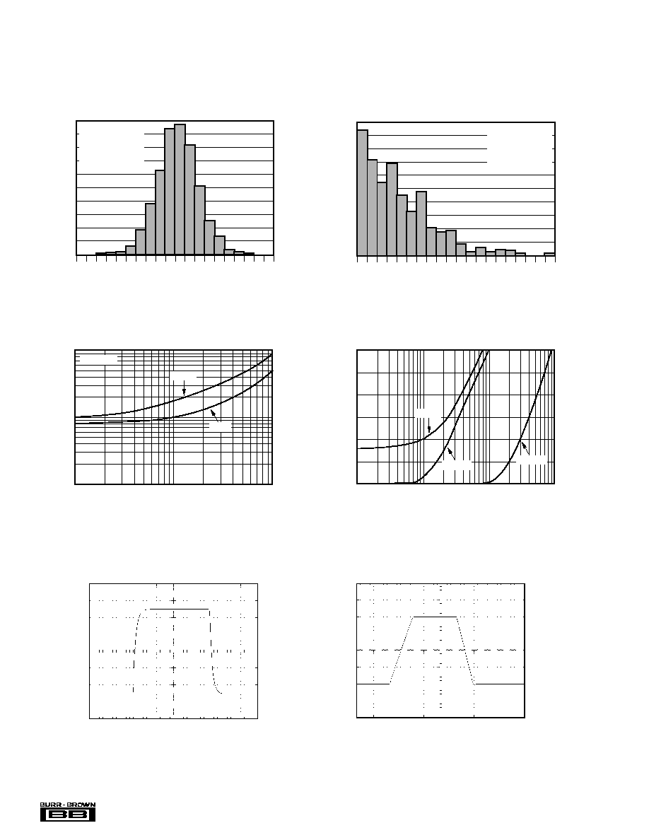
SMALL-SIGNAL STEP RESPONSE
G = 1, C
L
= 50pF
20mV/div
1
µ
s/div
LARGE-SIGNAL STEP RESPONSE
G = 1, C
L
= 50pF
5V/div
5
µ
s/div
SMALL-SIGNAL OVERSHOOT
vs LOAD CAPACITANCE
Load Capacitance (pF)
Overshoot (%)
60
50
40
30
20
10
0
10
100
1k
10k
G = ≠1
G = +10
G = +1
OFFSET VOLTAGE PRODUCTION DISTRIBUTION
Percent of Amplifiers (%)
Offset Voltage (mV)
20
18
16
14
12
10
8
6
4
2
0
Typical production
distribution of
packaged units.
Single, duals, and
quads included.
≠10
≠9
≠8
≠7
≠6
≠5
≠4
≠3
≠2
≠1
0
1
2
3
4
5
6
7
8
9
10
SETTLING TIME vs CLOSED-LOOP GAIN
Closed-Loop Gain (V/V)
Settling Time (µs)
100
10
1
1
10
100
10V Step
0.01%
0.1%
OFFSET VOLTAGE DRIFT
PRODUCTION DISTRIBUTION
Percent of Amplifiers (%)
Offset Voltage Drift (
µ
V/
∞
C)
20
18
16
14
12
10
8
6
4
2
0
Typical production
distribution of
packaged units.
Single, duals, and
quads included.
0
4
8
12
16
20
24
28
32
36
40
44
48
52
56
60
64
68
82
76
80
7
Æ
OPA137, 2137, 4137
APPLICATIONS INFORMATION
OPA137 series op amps are unity-gain stable and suitable
for a wide range of general-purpose applications. Power
supply pins should be bypassed with 10nF ceramic capaci-
tors or larger. All circuitry is completely independent in dual
and quad versions, assuring normal performance when one
amplifier in a package is overdriven or short circuited. Many
key parameters are guaranteed over the specified tempera-
ture range, ≠40
∞
C to +85
∞
C.
OPERATING VOLTAGE
OPA137 op amps can be operated on power supplies as low
as
±
2.25V. Performance remains excellent with power sup-
plies ranging from
±
2.25V to
±
18V (+4.5V to +36V single
supply). Most parameters vary only slightly throughout this
supply voltage range. Quiescent current and short-circuit
current vs supply voltage are shown in Typical Performance
Curves.
Operation at very low supply voltage (V
S
±
3V) requires
careful attention to ensure that the common-mode voltage
remains within the linear range, V
CM
= (V≠)+3V to (V+).
Inputs may need to be biased above ground in accordance
with the common-mode voltage range restrictions for linear
operation.
INPUT VOLTAGE
The input common-mode voltage range of OPA137 series
op amps extends from (V≠)+3V to the positive rail, V+. For
normal operation, inputs should be limited to this range. The
inputs may go beyond the power supplies without output
phase-reversal. Many FET-input op amps (such as TL061
types) exhibit phase-reversal of the output when the input
common-mode range is exceeded. This can occur in voltage-
follower circuits, causing serious problems in control loop
applications.
Input terminals are diode-clamped to the power supply rails
for ESD protection. If the input voltage can exceed the
negative supply by 500mV, input current should be limited
to 2mA (or less). If the input current is not adequately
limited, you may see unpredicatable behavior in the other
amplifiers in the package. This is easily accomplished with
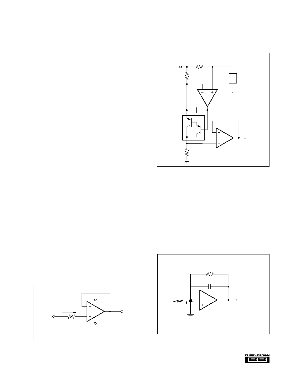
an input resistor as shown in Figure 1. Many input signals
are inherently current-limited, therefore, a limiting resistor
may not be required.
FIGURE 1. Input Current Protection for Voltages Exceed-
ing the Supply Voltage.
HIGH-SIDE CURRENT SENSING
Many applications require the sensing of signals near the
positive supply. The common-mode input range of OPA137
op amps includes the positive rail, enabling them to be used
to sense power supply currents as shown in Figure 2.
FIGURE 2. High-Side Current Monitor.
INPUT BIAS CURRENT
The input bias current is approximately 5pA at room tem-
perature and increases with temperature as shown in the
typical performance curve "Input Bias Current vs Tempera-
ture."
Input Bias current also varies with common-mode voltage
and power supply voltage. This variation is dependent on
the voltage between the negative power supply and the
common-mode input voltage. The effect is shown in the
typical performance curve "Input Bias Current vs Common-
Mode Voltage."
FIGURE 3. Photodetector Amplifier.
R
F
1M
3.3pF
V
O
= ≠ R
F
I
D
I
D
OPA137
I
D
is proportional to
light intensity (radiant power)
Photodiode
BPW34
C
D
= 75pF
OPA137
V
IN
V
OUT
I
OVERLOAD
2mA max
V≠
V+
Inputs are internally
clamped to V+ and V≠
R
1
0.1
R
2
1k
R
3
10k
OPA241
V
O
= I
L
OPA137
20pF
Load
Ground-referred
output
V
O
V+
R
1
R
3
R
2
Zetex
Darlington
ZTX712
8
Æ
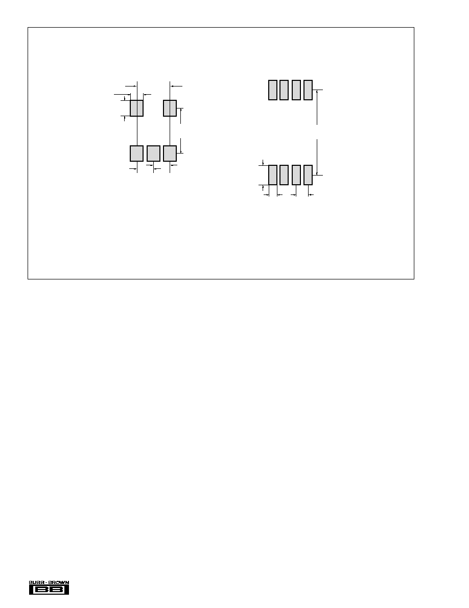
OPA137, 2137, 4137
FIGURE 4. Recommended SOT-23-5 and MSOP-8 Solder Footprints.
0.04
(1.016)
0.19
(4.83)
0.016
(0.41)
0.0256
(0.65)
MSOP-8
(Package Drawing #337)
SOT-23-5
(Package Drawing #331)
Refer to end of data sheet or Appendix C of Burr-Brown
Data Book for tolerances and detailed package drawing.
For further information on solder pads for surface-mount
devices consult Application Bulletin AB-132.
0.035
(0.889)
0.10
(2.54)
0.0375
(0.9525)
0.0375
(0.9525)
0.075
(1.905)
0.027
(0.686)

PACKAGING INFORMATION
ORDERABLE DEVICE
STATUS(1)
PACKAGE TYPE
PACKAGE DRAWING
PINS
PACKAGE QTY
OPA137N/250
ACTIVE
SOP
DBV
5
250
OPA137N/3K
ACTIVE
SOP
DBV
5
3000
OPA137NA/250
ACTIVE
SOP
DBV
5
250
OPA137NA/3K
ACTIVE
SOP
DBV
5
3000
OPA137P
ACTIVE
PDIP
P
8
50
OPA137PA
ACTIVE
PDIP
P
8
50
OPA137U
ACTIVE
SOIC
D
8
100
OPA137U/2K5
ACTIVE
SOIC
D
8
2500
OPA137UA
ACTIVE
SOIC
D
8
100
OPA137UA/2K5
ACTIVE
SOIC
D
8
2500
OPA2137E/250
ACTIVE
VSSOP
DGK
8
250
OPA2137E/2K5
ACTIVE
VSSOP
DGK
8
2500
OPA2137EA/250
ACTIVE
VSSOP
DGK
8
250
OPA2137EA/2K5
ACTIVE
VSSOP
DGK
8
2500
OPA2137P
ACTIVE
PDIP
P
8
50
OPA2137PA
ACTIVE
PDIP
P
8
50
OPA2137U
ACTIVE
SOIC
D
8
100
OPA2137U/2K5
ACTIVE
SOIC
D
8
2500
OPA2137UA
ACTIVE
SOIC
D
8
100
OPA2137UA/2K5
ACTIVE
SOIC
D
8
2500
OPA4137P
ACTIVE
PDIP
N
14
25
OPA4137PA
ACTIVE
PDIP
N
14
25
OPA4137U
ACTIVE
SOIC
D
14
58
OPA4137U/2K5
ACTIVE
SOIC
D
14
2500
OPA4137UA
ACTIVE
SOIC
D
14
58
OPA4137UA/2K5
ACTIVE
SOIC
D
14
2500
(1) The marketing status values are defined as follows:
ACTIVE: Product device recommended for new designs.
LIFEBUY: TI has announced that the device will be discontinued, and a lifetime-buy period is in effect.
NRND: Not recommended for new designs. Device is in production to support existing customers, but TI does not recommend using this part in
a new design.
PREVIEW: Device has been announced but is not in production. Samples may or may not be available.
OBSOLETE: TI has discontinued the production of the device.
PACKAGE OPTION ADDENDUM
www.ti.com
3-Oct-2003

IMPORTANT NOTICE
Texas Instruments Incorporated and its subsidiaries (TI) reserve the right to make corrections, modifications,
enhancements, improvements, and other changes to its products and services at any time and to discontinue
any product or service without notice. Customers should obtain the latest relevant information before placing
orders and should verify that such information is current and complete. All products are sold subject to TI's terms
and conditions of sale supplied at the time of order acknowledgment.
TI warrants performance of its hardware products to the specifications applicable at the time of sale in
accordance with TI's standard warranty. Testing and other quality control techniques are used to the extent TI
deems necessary to support this warranty. Except where mandated by government requirements, testing of all
parameters of each product is not necessarily performed.
TI assumes no liability for applications assistance or customer product design. Customers are responsible for
their products and applications using TI components. To minimize the risks associated with customer products
and applications, customers should provide adequate design and operating safeguards.
TI does not warrant or represent that any license, either express or implied, is granted under any TI patent right,
copyright, mask work right, or other TI intellectual property right relating to any combination, machine, or process
in which TI products or services are used. Information published by TI regarding third-party products or services
does not constitute a license from TI to use such products or services or a warranty or endorsement thereof.
Use of such information may require a license from a third party under the patents or other intellectual property
of the third party, or a license from TI under the patents or other intellectual property of TI.
Reproduction of information in TI data books or data sheets is permissible only if reproduction is without
alteration and is accompanied by all associated warranties, conditions, limitations, and notices. Reproduction
of this information with alteration is an unfair and deceptive business practice. TI is not responsible or liable for
such altered documentation.
Resale of TI products or services with statements different from or beyond the parameters stated by TI for that
product or service voids all express and any implied warranties for the associated TI product or service and
is an unfair and deceptive business practice. TI is not responsible or liable for any such statements.
Following are URLs where you can obtain information on other Texas Instruments products and application
solutions:
Products
Applications
Amplifiers
amplifier.ti.com
Audio
www.ti.com/audio
Data Converters
dataconverter.ti.com
Automotive
www.ti.com/automotive
DSP
dsp.ti.com
Broadband
www.ti.com/broadband
Interface
interface.ti.com
Digital Control
www.ti.com/digitalcontrol
Logic
logic.ti.com
Military
www.ti.com/military
Power Mgmt
power.ti.com
Optical Networking
www.ti.com/opticalnetwork
Microcontrollers
microcontroller.ti.com
Security
www.ti.com/security
Telephony
www.ti.com/telephony
Video & Imaging
www.ti.com/video
Wireless
www.ti.com/wireless
Mailing Address:
Texas Instruments
Post Office Box 655303 Dallas, Texas 75265
Copyright
2003, Texas Instruments Incorporated