Document Outline
- FEATURES
- APPLICATIONS
- DESCRIPTION
- ABSOLUTE MAXIMUM RATINGS
- PACKAGE/ORDERING INFORMATION
- ELECTRICAL CHARACTERISTICS: V S = 2.5V to 5.5V
- TYPICAL CHARACTERISTICS
- APPLICATIONS INFORMATION
- OPERATING VOLTAGE
- RAIL-TO-RAIL INPUT
- DESIGN OPTIMIZATION WITH RAIL- TO- RAIL INPUT OP AMPS
- COMMON-MODE REJECTION
- INPUT VOLTAGE
- RAIL-TO-RAIL OUTPUT
- CAPACITIVE LOAD AND STABILITY
- DRIVING ADCs
- OPA2347 WCSP PACKAGE
- PHOTOSENSITIVITY
- PACKAGE DIMENSIONS
- LAND PATTERNS AND ASSEMBLY
- RELIABILITY TESTING
- PACKAGE DRAWINGS
- DBV (R=PDSO-G5) PLASTICE SMALL-OUTLINE
- P(R-PDIP-T8) PLASTIC DUAL-IN-LINE
- D(R-PDSO-G**) PLASTIC SMALL-OUTLINE PACKAGE
- DCK (R-PDSO-G5) PLASTIC SMALL-OUTLINE
- DCN (R-PDSO-G8) PLASTIC SMALL-OUTLINE
- YED (P-XBGA-N8)DIE-SIZE BALL GRID ARRAY
- PW (R-PDSO-G**) PLASTIC SMALL-OUTLINE PACKAGE

micro
Power, Rail-to-Rail
Operational Amplifiers
FEATURES
q
LOW I
Q
: 20
µ
A
q
micro
SIZE PACKAGES: WCSP-8, SC70-5
SOT23-5, SOT23-8, and TSSOP-14
q
HIGH SPEED/POWER RATIO WITH
BANDWIDTH: 350kHz
q
RAIL-TO-RAIL INPUT AND OUTPUT
q
SINGLE SUPPLY: 2.3V to 5.5V
APPLICATIONS
q
PORTABLE EQUIPMENT
q
BATTERY-POWERED EQUIPMENT
q
2-WIRE TRANSMITTERS
q
SMOKE DETECTORS
q
CO DETECTORS
DESCRIPTION
The OPA347 is a
microPower, low-cost operational amplifier
available in
micropackages. The OPA347 (single version) is
available in the SC-70 and SOT23-5 packages. The OPA2347
(dual version) is available in the SOT23-8 and WCSP-8
packages. Both are also available in the SO-8. The OPA347
is also available in the DIP-8. The OPA4347 (quad) is
available in the SO-14 and the TSSOP-14.
The small size and low power consumption (34
µ
A per chan-
nel maximum) of the OPA347 make it ideal for portable and
battery-powered applications. The input range of the OPA347
extends 200mV beyond the rails, and the output range is
within 5mV of the rails. The OPA347 also features an
excellent speed/power ratio with a bandwidth of 350kHz.
The OPA347 can be operated with a single or dual power
supply from 2.3V to 5.5V. All models are specified for
operation from ≠55
∞
C to +125
∞
C.
Æ
OPA347
OPA347
OPA2347
OPA4347
OPA347
1
2
3
5
4
V+
≠In
Out
V≠
+In
OPA347
SOT23-5
1
2
3
4
8
7
6
5
NC
V+
Out
NC
NC
≠In
+In
V≠
OPA347
SO-8, DIP-8
1
2
3
4
8
7
6
5
V+
Out B
≠In B
+In B
Out A
≠In A
+In A
V≠
OPA2347
SOT23-8, SO-8
A
B
1
2
3
4
5
6
7
14
13
12
11
10
9
8
Out D
≠In D
+In D
V≠
+In C
≠In C
Out C
Out A
≠In A
+In A
V+
+In B
≠In B
Out B
OPA4347
TSSOP-14, SO-14
A
D
B
C
OPA347
OPA2347
OPA4347
SBOS167C ≠ NOVEMBER 2000≠ REVISED JUNE 2003
www.ti.com
PRODUCTION DATA information is current as of publication date.
Products conform to specifications per the terms of Texas Instruments
standard warranty. Production processing does not necessarily include
testing of all parameters.
Copyright © 2000-2003, Texas Instruments Incorporated
1
2
3
5
4
V+
Out
+In
V≠
≠In
OPA347
SC70-5
Please be aware that an important notice concerning availability, standard warranty, and use in critical applications of
Texas Instruments semiconductor products and disclaimers thereto appears at the end of this data sheet.
All trademarks are the property of their respective owners.
1
2
3
4
1
8
7
6
5
V+
Out B
≠In B
+In B
Out A
≠In A
+In A
V≠
OPA2347
(bump side down)
Not to Scale
WCSP-8
(top view)

OPA347, 2347, 4347
2
SBOS167C
www.ti.com
SPECIFIED
PACKAGE
TEMPERATURE
PACKAGE
ORDERING
TRANSPORT
PRODUCT
PACKAGE
DESIGNATOR
(1)
RANGE
MARKING
NUMBER
MEDIA, QUANTITY
OPA347NA
SOT23-5
DBV
≠55
∞
C to +125
∞
C
A47
OPA347NA/250
Tape and Reel, 250
"
"
"
"
"
OPA347NA /3K
Tape and Reel, 3000
OPA347PA
DIP-8
P
≠55
∞
C to +125
∞
C
OPA347PA
OPA347PA
Rails, 50
OPA347UA
SO-8
D
≠55
∞
C to +125
∞
C
OPA347UA
OPA347UA
Rails, 100
"
"
"
"
"
OPA347UA /2K5
Tape and Reel, 2500
OPA347SA
SC-70
DCK
≠55
∞
C to +125
∞
C
S47
OPA347SA/250
Tape and Reel, 250
"
"
"
"
"
OPA347SA/3K
Tape and Reel, 3000
OPA2347EA
SOT23-8
DCN
≠55
∞
C to +125
∞
C
B47
OPA2347EA /250
Tape and Reel, 250
"
"
"
"
"
OPA2347EA /3K
Tape and Reel, 3000
OPA2347UA
SO-8
D
≠55
∞
C to +125
∞
C
OPA2347UA
OPA2347UA
Rails, 100
"
"
"
"
"
OPA2347UA /2K5
Tape and Reel, 2500
OPA2347YED
WCSP-8
YED
≠55
∞
C to +125
∞
C
YMD CCS
OPA2347YEDT
Tape and Reel, 250
"
"
"
"
"
OPA2347YEDR
Tape and Reel, 3000
OPA4347EA
TSSOP-14
PW
≠55
∞
C to +125
∞
C
OPA4347EA
OPA4347EA /250
Tape and Reel, 250
"
"
"
"
"
OPA4347EA /2K5
Tape and Reel, 2500
OPA4347UA
SO-14
D
≠55
∞
C to +125
∞
C
OPA4347UA
OPA4347UA
Rails, 58
"
"
"
"
"
OPA4347UA /2K5
Tape and Reel, 2500
NOTE: (1) For the most current specifications and package information, refer to our web site at www.ti.com.
PACKAGE/ORDERING INFORMATION
Supply Voltage, V+ to V≠ ................................................................... 7.5V
Signal Input Terminals, Voltage
(2)
.................. (V≠) ≠ 0.5V to (V+) + 0.5V
Current
(2)
.................................................... 10mA
Output Short-Circuit
(3)
.............................................................. Continuous
Operating Temperature .................................................. ≠65
∞
C to +150
∞
C
Storage Temperature ..................................................... ≠65
∞
C to +150
∞
C
Junction Temperature ...................................................................... 150
∞
C
Lead Temperature (soldering, 10s) ................................................. 300
∞
C
NOTES: (1) Stresses above these ratings may cause permanent damage.
Exposure to absolute maximum conditions for extended periods may
degrade device reliability. These are stress ratings only. Functional opera-
tion of the device at these conditions, or beyond the specified operating
conditions, is not implied. (2) Input terminals are diode-clamped to the
power-supply rails. Input signals that can swing more than 0.5V beyond the
supply rails should be current-limited to 10mA or less. (3) Short-circuit to
ground, one amplifier per package.
ABSOLUTE MAXIMUM RATINGS
(1)
ELECTROSTATIC
DISCHARGE SENSITIVITY
This integrated circuit can be damaged by ESD. Texas Instru-
ments recommends that all integrated circuits be handled with
appropriate precautions. Failure to observe proper handling
and installation procedures can cause damage.
ESD damage can range from subtle performance degrada-
tion to complete device failure. Precision integrated circuits
may be more susceptible to damage because very small
parametric changes could cause the device not to meet its
published specifications.

OPA347, 2347, 4347
3
SBOS167C
www.ti.com
OPA347NA, UA, PA, SA
OPA2347EA, UA, YED
OPA4347EA, UA
PARAMETER
CONDITION
MIN
TYP
MAX
UNITS
OFFSET VOLTAGE
Input Offset Voltage
V
OS
V
S
= 5.5V, V
CM
= (V≠) + 0.8V
2
6
mV
over Temperature
2
7
mV
Drift
dV
OS
/dT
3
µ
V/
∞
C
vs Power Supply
PSRR
V
S
= 2.5V to 5.5V, V
CM
< (V+) ≠ 1.7V
60
175
µ
V/V
over Temperature
V
S
= 2.5V to 5.5V, V
CM
< (V+) ≠ 1.7V
300
µ
V/V
Channel Separation, DC
0.3
µ
V/V
f = 1kHz
128
dB
INPUT VOLTAGE RANGE
Common-Mode Voltage Range
V
CM
(V≠) ≠ 0.2
(V+) + 0.2
V
Common-Mode Rejection Ratio
CMRR
V
S
= 5.5V, (V≠) ≠ 0.2V < V
CM
< (V+) ≠ 1.7V
70
80
dB
over Temperature
V
S
= 5.5V, V≠ < V
CM
< (V+) ≠ 1.7V
66
dB
Vs = 5.5V, (V≠) ≠ 0.2V < V
CM
< (V+) + 0.2V
54
70
dB
over Temperature
Vs = 5.5V, V≠ < V
CM
< V+
48
dB
INPUT BIAS CURRENT
(1)
Input Bias Current
I
b
±
0.5
±
10
pA
Input Offset Current
I
OS
±
0.5
±
10
pA
INPUT IMPEDANCE
Differential
10
13
|| 3
|| pF
Common-Mode
10
13
|| 6
|| pF
NOISE
V
CM
< (V+) ≠ 1.7V
Input Voltage Noise, f = 0.1Hz to 10Hz
12
µ
V
PP
Input Voltage Noise Density, f = 1kHz
e
n
60
nV/
Hz
Input Current Noise Density, f = 1kHz
i
n
0.7
fA/
Hz
OPEN-LOOP GAIN
Open-Loop Voltage Gain
A
OL
V
S
= 5.5V, R
L
= 100k
, 0.015V < V
O
< 5.485V
100
115
dB
over Temperature
V
S
= 5.5V, R
L
= 100k
, 0.015V < V
O
< 5.485V
88
dB
V
S
= 5.5V, R
L
= 5k
, 0.125V < V
O
< 5.375V
100
115
dB
over Temperature
V
S
= 5.5V, R
L
= 5k
, 0.125V < V
O
< 5.375V
88
dB
A
OL
(SC-70 only)
V
S
= 5.5V, R
L
= 5k
0.125V < V
O
< 5.375V
96
115
dB
OUTPUT
Voltage Output Swing from Rail
R
L
= 100k
, A
OL
> 100dB
5
15
mV
over Temperature
R
L
= 100k
, A
OL
> 88dB
15
mV
R
L
= 5k
, A
OL
> 100dB
90
125
mV
over Temperature
R
L
= 5k
, A
OL
> 88dB
125
mV
Short-Circuit Current
I
SC
±
17
mA
Capacitive Load Drive
C
LOAD
See Typical Characteristics
FREQUENCY RESPONSE
C
L
= 100pF
Gain-Bandwidth Product
GBW
350
kHz
Slew Rate
SR
G = +1
0.17
V/
µ
s
Settling Time, 0.1%
t
S
V
S
= 5V, 2V Step, G = +1
21
µ
s
0.01%
V
S
= 5V, 2V Step, G = +1
27
µ
s
Overload Recovery Time
V
IN
◊
Gain = V
S
23
µ
s
POWER SUPPLY
Specified Voltage Range
V
S
2.5
5.5
V
Minimum Operating Voltage
2.3
V
Minimum Operating Voltage (OPA347SA)
2.4
V
Quiescent Current (per amplifier)
I
Q
I
O
= 0
20
34
µ
A
over Temperature
38
µ
A
TEMPERATURE RANGE
Specified Range
≠55
125
∞
C
Operating Range
≠65
150
∞
C
Storage Range
≠65
150
∞
C
Thermal Resistance
JA
SOT23-5 Surface-Mount
200
∞
C/W
SOT23-8 Surface-Mount
150
∞
C/W
SO-8 Surface-Mount
150
∞
C/W
SO-14 Surface-Mount
100
∞
C/W
TSSOP-14 Surface-Mount
100
∞
C/W
DIP-8
100
∞
C/W
SC70-5 Surface-Mount
250
∞
C/W
ELECTRICAL CHARACTERISTICS: V
S
= 2.5V to 5.5V
Boldface limits apply over the specified temperature range, T
A
= ≠55
∞
C to +125
∞
C.
At T
A
= +25
∞
C, R
L
= 100k
connected to V
S
/2 and V
OUT
= V
S
/2, unless otherwise noted.
NOTE: (1) Input bias current for the OPA2347YED package is specified in the absence of light. See the Photosensitivity section for further detail.

OPA347, 2347, 4347
4
SBOS167C
www.ti.com
TYPICAL CHARACTERISTICS
At T
A
= +25
∞
C, V
S
= +5V, and R
L
= 100k
connected to V
S
/2, unless otherwise noted.
OPEN-LOOP GAIN/PHASE vs FREQUENCY
10
Open-Loop Gain (dB)
0
≠30
≠60
≠90
≠120
≠150
≠180
Phase (
∞
)
Frequency (Hz)
100
1k
10k
100k
1M
100
80
60
40
20
0
≠20
POWER-SUPPLY AND COMMON-MODE
REJECTION vs FREQUENCY
10
PSRR, CMRR (dB)
Frequency (Hz)
100
1k
10k
100k
1M
100
80
60
40
20
0
CMRR
PSRR
MAXIMUM OUTPUT VOLTAGE vs FREQUENCY
Output Voltage (Vp-p)
Frequency (Hz)
1k
10k
100k
1M
6
5
4
3
2
1
0
V
S
= 5.5V
V
S
= 5.0V
V
S
= 2.5V
CHANNEL SEPARATION vs FREQUENCY
10
Channel Separation (dB)
Frequency (Hz)
100
1k
10k
100k
1M
140
120
100
80
60
OUTPUT VOLTAGE SWING vs OUTPUT CURRENT
0
Output Voltage (V)
Output Current (
±
mA)
5
10
15
20
25
V+
(V+) ≠ 1
(V+) ≠ 2
2
1
0
Sourcing
Sinking
125
∞
C
25
∞
C
≠55
∞
C
≠55
∞
C
QUIESCENT AND SHORT-CIRCUIT CURRENT
vs SUPPLY VOLTAGE
2.0
Quiescent Current (
µ
A)
25
20
15
10
5
Short-Circuit Current (mA)
Supply Voltage (V)
2.5
3.0
3.5
4.0
4.5
5.0
5.5
30
25
20
15
10
I
Q
I
SC

OPA347, 2347, 4347
5
SBOS167C
www.ti.com
TYPICAL CHARACTERISTICS
(Cont.)
At T
A
= +25
∞
C, V
S
= +5V, and R
L
= 100k
connected to V
S
/2, unless otherwise noted.
OPEN-LOOP GAIN AND POWER-SUPPLY
REJECTION vs TEMPERATURE
≠75
A
OL
, PSRR (dB)
Temperature (
∞
C)
≠50
≠25
0
25
50
75
100
125
150
130
120
110
100
90
80
70
A
OL
PSRR
QUIESCENT AND SHORT-CIRCUIT CURRENT
vs TEMPERATURE
≠75
Quiescent Current (
µ
A)
25
20
15
10
5
Short-Circuit Current (mA)
Temperature (
∞
C)
≠50
≠25
0
25
50
75
100
125
150
30
25
20
15
10
I
SC
I
Q
INPUT BIAS CURRENT vs TEMPERATURE
≠75
Input Bias Current (pA)
Temperature (
∞
C)
≠50
≠25
0
25
50
75
100
125
150
10k
1k
100
10
1
0.1
≠6
≠5
≠4
≠3
≠2
≠1
0
1
2
3
4
5
6
OFFSET VOLTAGE PRODUCTION DISTRIBUTION
Offset Voltage (mV)
18
16
14
12
10
8
6
4
2
0
Percent of Amplifiers (%)
Typical production
distribution of
packaged units.
COMMON-MODE REJECTION vs TEMPERATURE
≠75
Common-Mode Rejection (dB)
Temperature (
∞
C)
≠50
≠25
0
25
50
75
100
125
150
100
90
80
70
60
50
40
V≠ < V
CM
< (V+) ≠ 1.7V
V≠ < V
CM
< V+
OFFSET VOLTAGE DRIFT MAGNITUDE
PRODUCTION DISTRIBUTION
Percentage of Amplifiers (%)
Offset Voltage Drift (
µ
V/
∞
C)
1
2
3
4
5
6
7
8
9
10
11
12
25
20
15
10
5
0

OPA347, 2347, 4347
6
SBOS167C
www.ti.com
SMALL-SIGNAL STEP RESPONSE
G = +1V/V, R
L
= 100k
, C
L
= 100pF
20mV/div
10
µ
s/div
SMALL-SIGNAL STEP RESPONSE
G = +1V/V, R
L
= 5k
, C
L
= 100pF
20mV/div
10
µ
s/div
INPUT VOLTAGE AND CURRENT NOISE
SPECTRAL DENSITY vs FREQUENCY
1
Voltage Noise (nV/
Hz)
Current Noise (fA
Hz)
Frequency (Hz)
10
100
1k
10k
100k
10k
1k
100
10
100
10
1.0
0.1
TYPICAL CHARACTERISTICS
(Cont.)
At T
A
= +25
∞
C, V
S
= +5V, and R
L
= 100k
connected to V
S
/2, unless otherwise noted.
SMALL-SIGNAL OVERSHOOT
vs LOAD CAPACITANCE
10
Small-Signal Overshoot (%)
Load Capacitance (pF)
100
1k
10k
60
50
40
30
20
10
0
G = +1V/V
R
L
= 100k
G = ≠1V/V
R
FB
= 5k
G = ≠1V/V
R
FB
= 100k
SMALL-SIGNAL OVERSHOOT
vs LOAD CAPACITANCE
10
Small-Signal Overshoot (%)
Load Capacitance (pF)
100
1k
10k
50
40
30
20
10
0
G =
±
5V/V
R
FB
= 100k
LARGE-SIGNAL STEP RESPONSE
G = +1V/V, R
L
= 100k
, C
L
= 100pF
500mV/div
20
µ
s/div
OPA347, 2347, 4347
7
SBOS167C
www.ti.com
APPLICATIONS INFORMATION
The OPA347 series op amps are unity-gain stable and can
operate on a single supply, making them highly versatile and
easy to use.
Rail-to-rail input and output swing significantly increases dy-
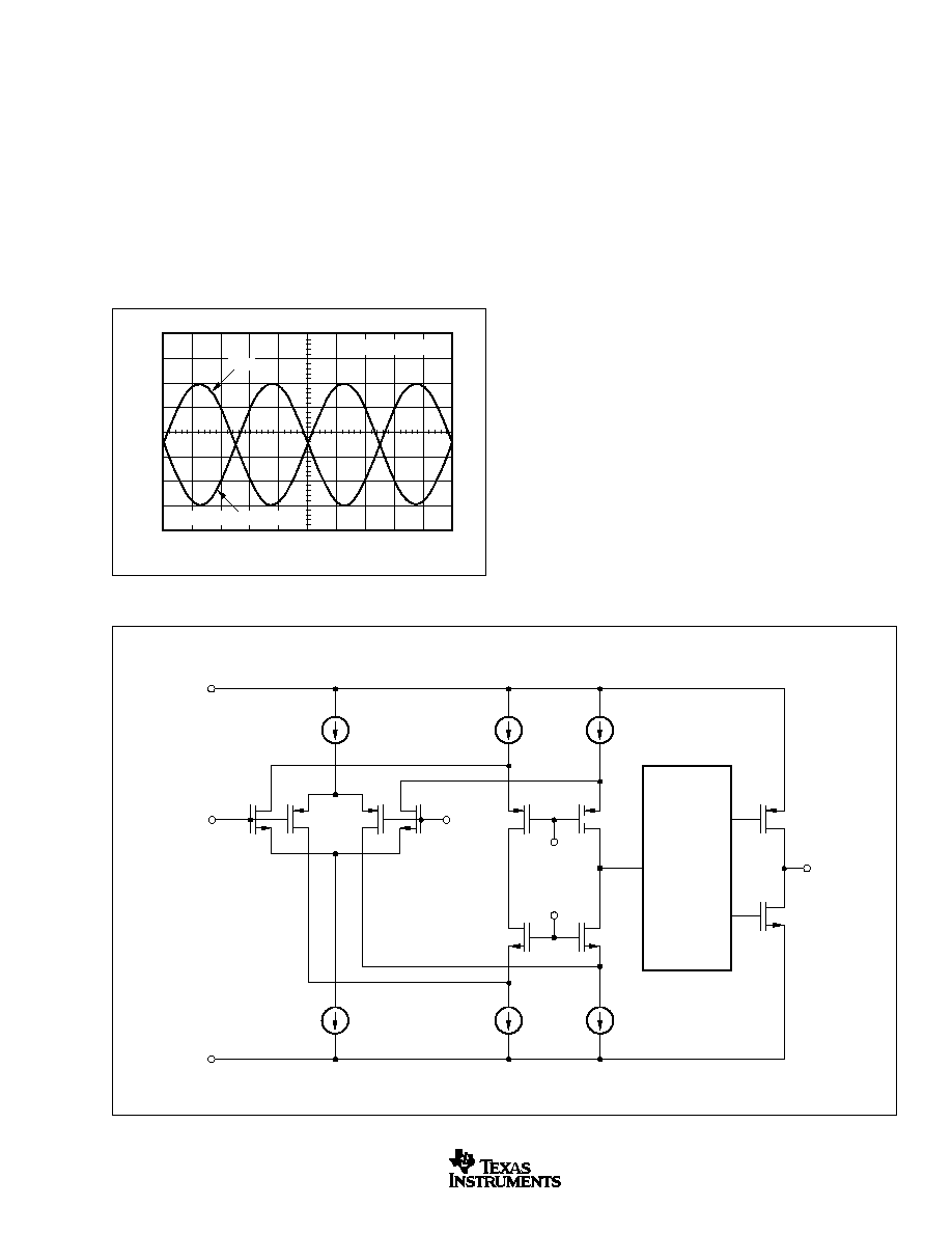
namic range, especially in low supply applications. Figure 1
shows the input and output waveforms for the OPA347 in
unity-gain configuration. Operation is from V
S
= +5V with a
100k
load connected to V
S
/2. The input is a 5V
PP
sinusoid.
Output voltage is approximately 4.995V
PP
.
Power-supply pins should be bypassed with 0.01
µ
F ceramic
capacitors.
OPERATING VOLTAGE
The OPA347 series op amps are fully specified and en-
sured from 2.5V to 5.5V. In addition, many specifications
apply from ≠55
∞
C to +125
∞
C. Parameters that vary signifi-
cantly with operating voltages or temperature are shown in
the Typical Characteristics.
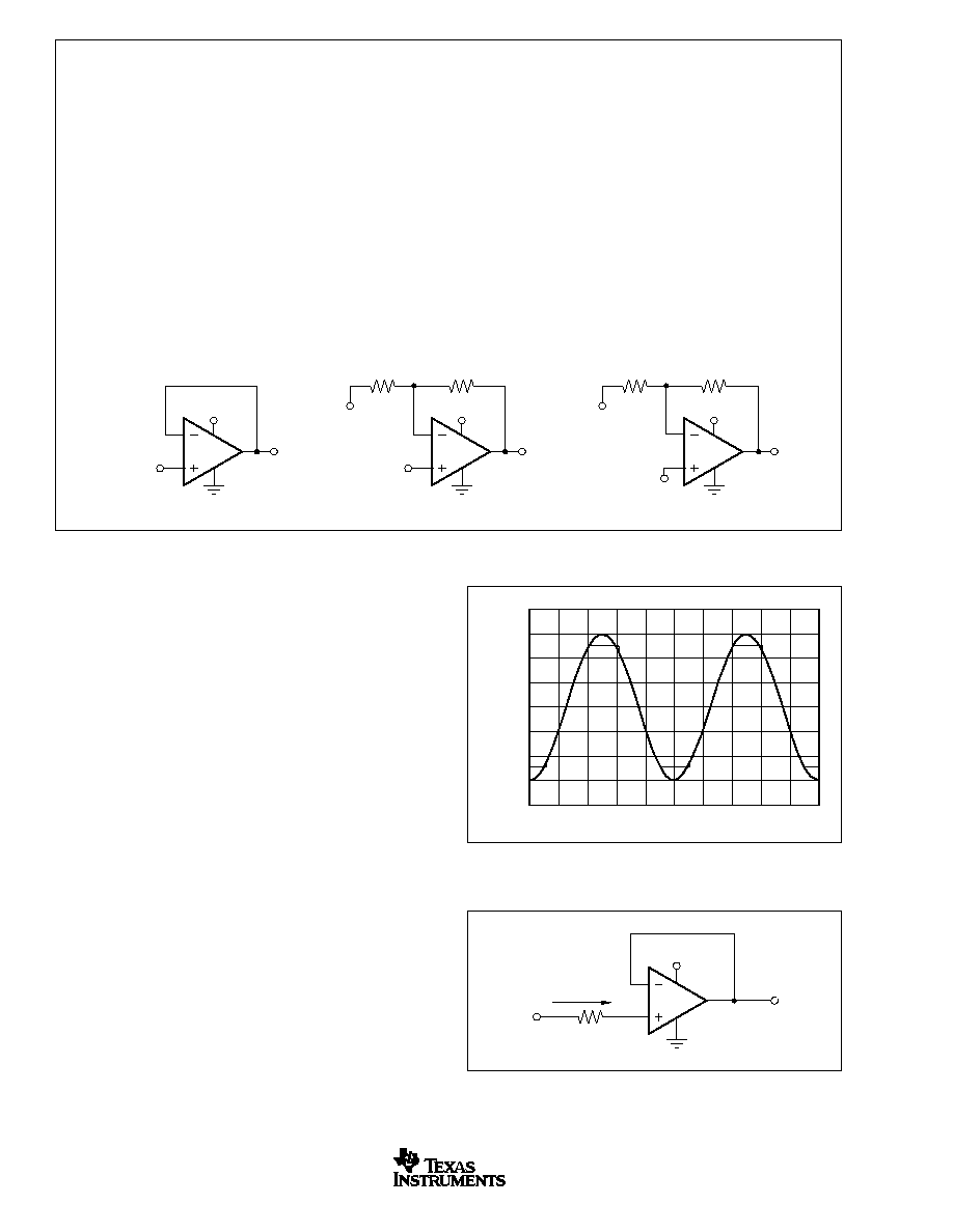
RAIL-TO-RAIL INPUT
The input common-mode voltage range of the OPA347
series extends 200mV beyond the supply rails. This is
achieved with a complementary input stage--an N-channel
input differential pair in parallel with a P-channel differential
pair, as shown in Figure 2. The N-channel pair is active for
input voltages close to the positive rail, typically (V+) ≠ 1.3V
to 200mV above the positive supply, while the P-channel pair
is on for inputs from 200mV below the negative supply to
approximately (V+) ≠ 1.3V. There is a small transition region,
typically (V+) ≠ 1.5V to (V+) ≠ 1.1V, in which both pairs are
on. This 400mV transition region can vary 300mV with
process variation. Thus, the transition region (both stages
on) can range from (V+) ≠ 1.65V to (V+) ≠ 1.25V on the low
end, up to (V+) ≠ 1.35V to (V+) ≠ 0.95V on the high end.
Within the 400mV transition region PSRR, CMRR, offset
voltage, and offset drift may be degraded compared to
operation outside this region. For more information on de-
signing with rail-to-rail input op amps, see Figure 3,
Design
Optimization with Rail-to-Rail Input Op Amps.
FIGURE 2. Simplified Schematic.
FIGURE 1. Rail-to-Rail Input and Output.
V
BIAS1
V
BIAS2
V
IN
+
V
IN
≠
Class AB
Control
Circuitry
V
O
V≠
(Ground)
V+
Reference
Current
Input
Output (inverted on scope)
5V
1V/div
0V
G = +1, V
S
= +5V
20
µ
s/div
OPA347, 2347, 4347
8
SBOS167C
www.ti.com
COMMON-MODE REJECTION
The CMRR for the OPA347 is specified in several ways so
the best match for a given application may be used. First, the
CMRR of the device in the common-mode range below the
transition region (V
CM
< (V+) ≠ 1.7V) is given. This specifica-
tion is the best indicator of the capability of the device when
the application requires use of one of the differential input
pairs. Second, the CMRR at V
S
= 5.5V over the entire
common-mode range is specified.
INPUT VOLTAGE
The input common-mode range extends from (V≠) ≠ 0.2V to
(V+) + 0.2V. For normal operation, inputs should be limited
to this range. The absolute maximum input voltage is 500mV
beyond the supplies. Inputs greater than the input
common-mode range but less than the maximum input
voltage, while not valid, will not cause any damage to the op
amp. Furthermore, if input current is limited the inputs may go
beyond the power supplies without phase inversion, as
shown in Figure 4, unlike some other op amps.
Normally, input currents are 0.4pA. However, large inputs
(greater than 500mV beyond the supply rails) can cause
excessive current to flow in or out of the input pins. There-
fore, as well as keeping the input voltage below the maxi-
mum rating, it is also important to limit the input current to
less than 10mA. This is easily accomplished with an input
resistor, as shown in Figure 5.
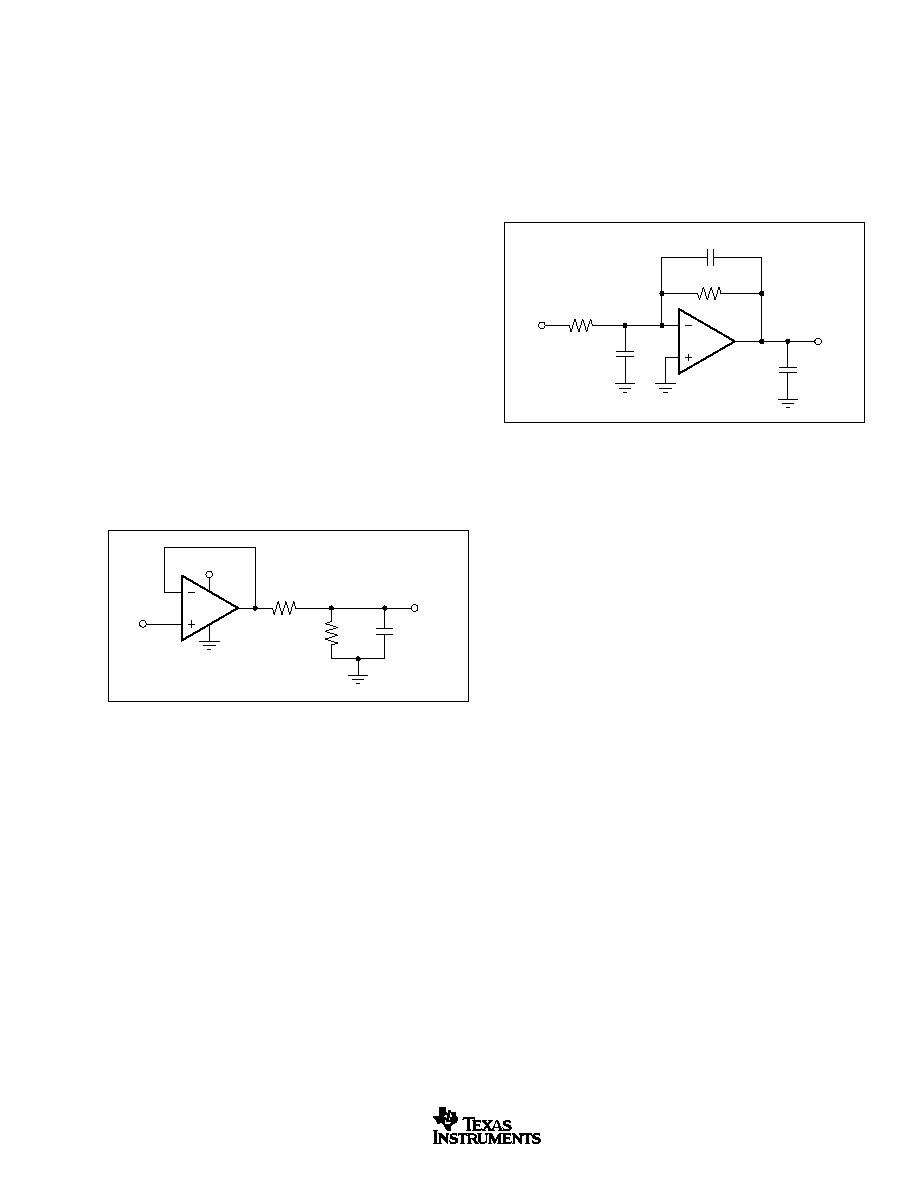
FIGURE 3. Design Optimization with Rail-to-Rail Input Op Amps.
Rail-to-rail op amps can be used in virtually any op amp
configuration. To achieve optimum performance, how-
ever, applications using these special double-input-stage
op amps may benefit from consideration of their special
behavior.
In many applications, operation remains within the com-
mon-mode range of only one differential input pair. How-
ever, some applications exercise the amplifier through the
transition region of both differential input stages. A small
discontinuity may occur in this transition. Careful selection
of the circuit configuration, signal levels, and biasing can
often avoid this transition region.
DESIGN OPTIMIZATION WITH RAIL-TO-RAIL INPUT OP AMPS
With a unity-gain buffer, for example, signals will traverse
this transition at approximately 1.3V below the V+ supply
and may exhibit a small discontinuity at this point.
The common-mode voltage of the noninverting amplifier
is equal to the input voltage. If the input signal always
remains less than the transition voltage, no discontinuity
will be created. The closed-loop gain of this configuration
can still produce a rail-to-rail output.
Inverting amplifiers have a constant common-mode volt-
age equal to V
B
. If this bias voltage is constant, no
discontinuity will be created. The bias voltage can gener-
ally be chosen to avoid the transition region.
FIGURE 4. OPA347--No Phase Inversion with Inputs Greater
than the Power-Supply Voltage.
V
O
V
IN
V
B
V+
Noninverting Amplifier
V
CM
= V
IN
V
O
V
B
V
IN
V+
Inverting Amplifier
V
CM
= V
B
V
O
V
IN
V+
Unity-Gain Buffer
V
CM
= V
IN
= V
O
FIGURE 5. Input Current Protection for Voltages Exceeding
the Supply Voltage.
5k
OPA347
10mA max
+5V
V
IN
V
OUT
I
OVERLOAD
5.5V
0V
≠0.5V
200
µ
s/div
OPA347, 2347, 4347
9
SBOS167C
www.ti.com
RAIL-TO-RAIL OUTPUT
A class AB output stage with common-source transistors is
used to achieve rail-to-rail output. This output stage is ca-
pable of driving 5k
loads connected to any potential be-
tween V+ and ground. For light resistive loads (> 100k
), the
output voltage can typically swing to within 5mV from supply
rail. With moderate resistive loads (10k
to 50k
), the output
can swing to within a few tens of millivolts from the supply
rails while maintaining high open-loop gain (see the typical
characteristic Output Voltage Swing vs Output Current).
CAPACITIVE LOAD AND STABILITY
The OPA347 in a unity-gain configuration can directly drive
up to 250pF pure capacitive load. Increasing the gain en-
hances the amplifier's ability to drive greater capacitive loads
(see the characteristic curve Small-Signal Overshoot vs
Capacitive Load). In unity-gain configurations, capacitive
load drive can be improved by inserting a small (10
to 20
)
resistor, R
S
, in series with the output, as shown in Figure 6.
This significantly reduces ringing while maintaining Direct
Current (DC) performance for purely capacitive loads. How-
ever, if there is a resistive load in parallel with the capacitive
load, a voltage divider is created, introducing a DC error at
the output and slightly reducing the output swing. The error
introduced is proportional to the ratio R
S
/ R
L
, and is generally
negligible.
load, reducing the resistor values from 100k
to 5k
de-
creases overshoot from 40% to 8% (see the characteristic
curve Small-Signal Overshoot vs Load Capacitance). How-
ever, when large-valued resistors can not be avoided, a
small (4pF to 6pF) capacitor, C
FB
, can be inserted in the
feedback, as shown in Figure 7. This significantly reduces
overshoot by compensating the effect of capacitance, C
IN
,
which includes the amplifier input capacitance and PC board
parasitic capacitance.
FIGURE 6. Series Resistor in Unity-Gain Buffer Configura-
tion Improves Capacitive Load Drive.
10
to
20
OPA347
V+
V
IN
V
OUT
R
S
R
L
C
L
FIGURE 7. Adding a Feedback Capacitor In the Unity-Gain
Inverter Configuration Improves Capacitative
Load.
R
I
OPA347
V
IN
V
OUT
R
F
C
FB
C
IN
C
L
DRIVING ADCs
The OPA347 series op amps are optimized for driving
medium-speed sampling Analog-to-Digital Converters (ADCs).
The OPA347 op amps buffer the ADC's input capacitance
and resulting charge injection while providing signal gain.
See Figure 8 for the OPA347 in a basic noninverting configu-
ration driving the ADS7822. The ADS7822 is a 12-bit,
microPower sampling converter in the MSOP-8 package.
When used with the low-power, miniature packages of the
OPA347, the combination is ideal for space-limited, low-
power applications. In this configuration, an RC network at
the ADC input can be used to provide for anti-aliasing filter
and charge injection current.
See Figure 9 for the OPA2347 driving an ADS7822 in a
speech bandpass filtered data acquisition system. This small,
low-cost solution provides the necessary amplification and
signal conditioning to interface directly with an electret micro-
phone. This circuit will operate with V
S
= 2.7V to 5V with less
than 250
µ
A typical quiescent current.
In unity-gain inverter configuration, phase margin can be
reduced by the reaction between the capacitance at the op
amp input, and the gain setting resistors, thus degrading
capacitive load drive. Best performance is achieved by using
small valued resistors. For example, when driving a 500pF

OPA347, 2347, 4347
10
SBOS167C
www.ti.com
FIGURE 8. OPA347 in Noninverting Configuration Driving ADS7822.
FIGURE 9. Speech Bandpass Filtered Data Acquisition System.
ADS7822
12-Bit ADC
DCLOCK
D
OUT
CS/SHDN
OPA347
+5V
V
IN
V+
2
+In
3
≠In
V
REF
8
4
GND
Serial
Interface
1
0.1
µ
F
0.1
µ
F
7
6
5
NOTE: ADC Input = 0V to V
REF
V
IN
= 0V to 5V for
0V to 5V output.
RC network filters high-frequency noise.
500
3300pF
C
3
33pF
V+
GND
3
1
8
4
5
6
7
≠IN
+IN
2
DCLOCK
Serial
Interface
C
2
1000pF
R
1
1.5k
R
4
20k
R
5
20k
R
6
100k
R
8
150k
R
9
510k
R
7
51k
D
OUT
V
REF
V+ = +2.7V to 5V
CS/SHDN
C
1
1000pF
Electret
Microphone
(1)
G = 100
Passband 300Hz to 3kHz
R
3
1M
R
2
1M
NOTE: (1) Electret microphone
powered by R
1
.
ADS7822
12-Bit A/D
1/2
OPA2347
1/2
OPA2347

OPA347, 2347, 4347
11
SBOS167C
www.ti.com
OPA2347 WCSP PACKAGE
The OPA2347YED is a die-level package using bump-on-pad
technology. Unlike plastic packages, the OPA2347YED has no
molding compound, lead frame, wire bonds, or leads. Using
standard surface-mount assembly procedures, the WCSP can
be mounted to a printed circuit board without additional under
fill. Figures 10 and 11 detail pinout and package marking.
FIGURE 10. Pin Description.
PACKAGE DIMENSIONS
The OPA2347YED is transported in tape and reel media and
is described in Table I and Figure 12. Pin 1 orientation is
consistent throughout the tape and reel carrier, with balls
facing down in each pocket of the carrier tape. The location
of Pin 1 is specified in Figure 12.
FIGURE 11. Top View Package Marking.
1
2
3
4
1
8
7
6
5
V+
Out B
≠In B
+In B
Out A
≠In A
+In A
V≠
OPA2347
(bump side down)
Not to Scale
WCSP-8
(top view)
1
OPA2347YED
Top View
YMDCCS
(bump side down)
Actual Size:
Package Marking Code:
YMD = year/month/day
CC = indicates OPA2347
S = for engineering purposes only
Exact Size:
1.008mm x 2.100mm
TEST
CONDITION
ACCEPT CRITERIA (ACTUAL)
SAMPLE SIZE
Temperature Cycle
≠40
∞
C to 125
∞
C, 1 Cycle/hr, 15 Minute Ramp
(1)
10 Minute Dwell
500 (1600) Cycles, R < 1.2X from R
0
36
Drop
50cm
10 (129) Drops, R < 1.2X from R
0
8
Key Push
100 Cycles/min,
5K (6.23K) Cycles, R < 1.2X from R
0
8
1300
µ
, Displacement = 2.7mm Max
3 Point Bend
Strain Rate 5 mm/min, 85 mm Span
R < 1.2X from R
0
8
NOTE: (1) Per IPC9701.
TABLE II. Reliability Test Results.
PHOTOSENSITIVITY
Although the OPA2347YED package has a protective back-
side coating that reduces the amount of light exposure on the
die, unless fully shielded, ambient light will still reach the
active region of the device. Input bias current for the
OPA2347YED package is specified in the absence of light.
Depending on the amount of light exposure in a given
application, an increase in bias current, and possible in-
creases in offset voltage should be expected. In circuit board
tests under ambient light conditions, a typical increase in bias
current reached 100pA. Flourescent lighting may introduce
noise or hum due to their time varying light output. Best
practice should include end-product packaging that provides
shielding from possible light souces during operation.
DIMENSIONS (mm)
OPA2347YED
Pocket Width, A
0
1.12
±
0.10
Pocket Length, B
0
2.13
±
0.10
Pocket Depth, K
0
0.61
±
0.10
Pocket Pitch, P
1
4.00
±
0.10
Sprocket Hole-to-Pocket Centerline, F
3.50
±
0.05
Sprocket Hole-to-Pocket Offset, P
2
2.00
±
0.05
Sprocket Hole Pitch, P
0
4.00
±
0.10
Tape Width, W
8.00
±
0.30
Reel Diameter, Max
TBD
TABLE I. Carrier Tape Dimensions.
FIGURE 12. Tape and Reel Carrier Tape Diagram.
+
+
+
+
+
+
+
+
+
+
+
+
+
5
∞
K
O
C
L
0.229
1.50
±
0.10
1.75
±
0.10
Y
Y
Pin 1
(1)
Section Y ≠ Y
Dimensions in mm
P
1
P
0
E
1
B
0
F
W
A
0
P
2
NOTE: (1) Pin 1 location is
in the upper left-hand corner
of the cavity. Units are shipped
with bumps down.
LAND PATTERNS AND ASSEMBLY
The recommended land pattern for the OPA2347YED package
is detailed in Figure 13 with specifications listed in Table III.
The maximum amount of force during assembly should be
limited to 30 grams of force per bump.
RELIABILITY TESTING
To ensure reliability, the OPA2347YED has been verified to
successfully pass a series of reliability stress tests. A sum-
mary of JEDEC standard reliability tests is shown in Table II.
OPA347, 2347, 4347
12
SBOS167C
www.ti.com
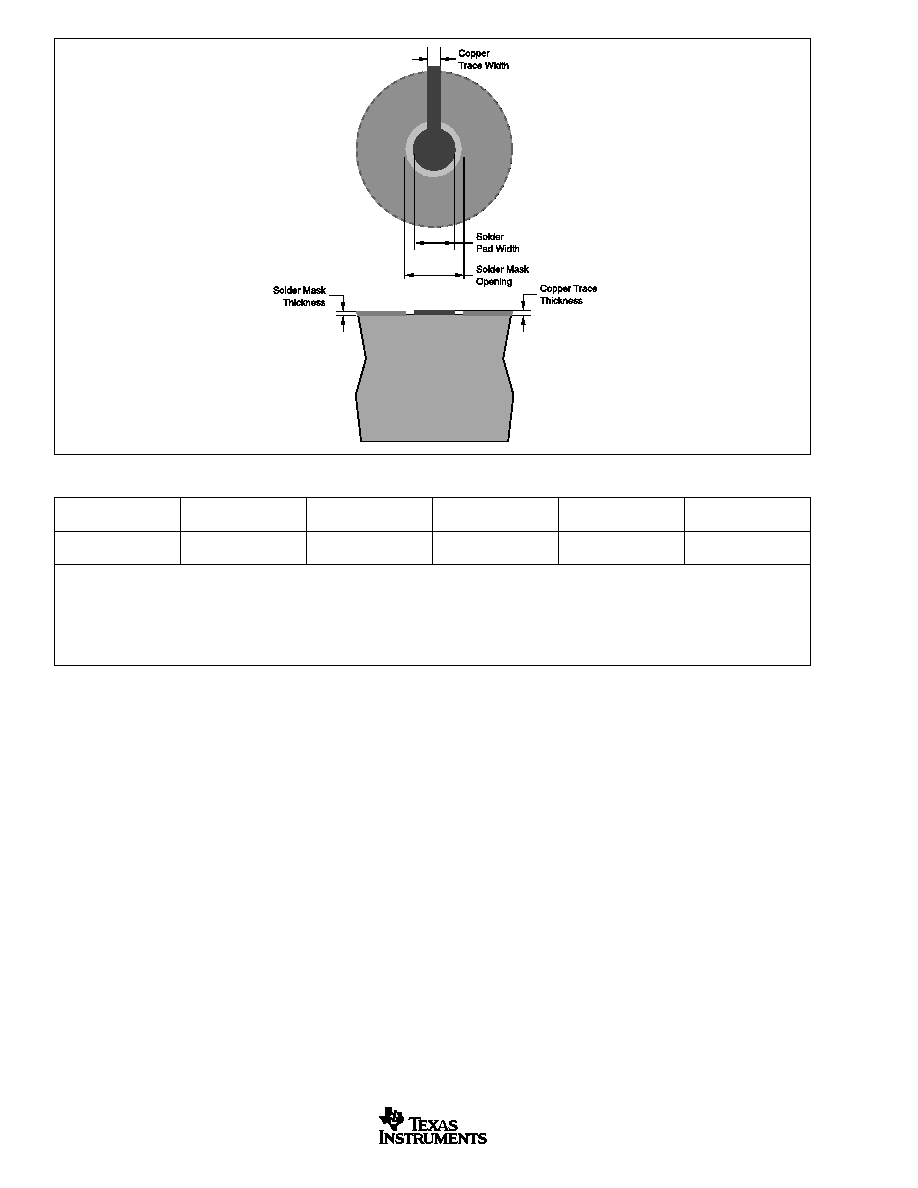
SOLDER PAD
SOLDER MASK
COPPER
DEFINITION
COPPER PAD
OPENING
THICKNESS
STENCIL OPENING
STENCIL THICKNESS
Non-Solder Mask
275
µ
m
375
µ
m
1 oz max
275
µ
m X 275
µ
m, sq
125
µ
m Thick
Defined (NSMD)
(+0.0, ≠25
µ
m)
(+0.0, ≠25
µ
m)
NOTES: (1) Circuit traces from NSMD-defined PWB lands should be less tham 100
µ
m (preferrably = 75
µ
m) wide in the exposed area inside the solder mask
opening. Wider trace widths will reduce device stand off and impact reliability. (2) Recommended solder paste is type 3 or type 4. (3) Best reliability results are
achieved when the PWB laminate glass transistion temperature is above the operating range of the intended application. (4) For PWB using an Ni/Au surface
finish, the gold thickness should be less than 0.5um to avoid solder embrittlement and a reduction in thermal fatigue performance. (5) Solder mask thickness
should be less than 20um on top of the copper circuit pattern. (6) Best solder stencil performance will be achieved using laser-cut stencils with electro polishing.
Use of chemically etched stencils results in inferior solder paste volume control. (7) Trace routing away from the WLCSP device should be balanced in X and
Y directions to avoid unintentional component movement due to solder wetting forces.
TABLE III. Recommended Land Pattern.
FIGURE 13. Recommended Land Area.

OPA347, 2347, 4347
13
SBOS167C
www.ti.com
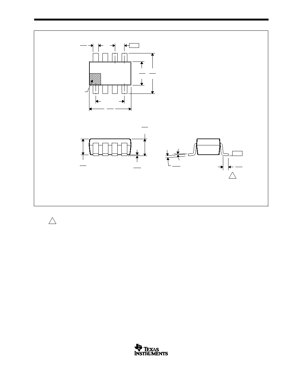
PACKAGE DRAWINGS
DBV (R-PDSO-G5)
PLASTIC SMALL-OUTLINE
0,10
M
0,20
0,95
0
∞
≠ 8
∞
0,25
0,35
0,55
Gage Plane
0,15 NOM
4073253-4/G 01/02
2,60
3,00
0,50
0,30
1,50
1,70
4
5
3
1
2,80
3,00
0,95
1,45
0,05 MIN
Seating Plane
NOTES: A. All linear dimensions are in millimeters.
B. This drawing is subject to change without notice.
C. Body dimensions do not include mold flash or protrusion.
D. Falls within JEDEC MO-178

OPA347, 2347, 4347
14
SBOS167C
www.ti.com
PACKAGE DRAWINGS (Cont.)
P (R-PDIP-T8)
PLASTIC DUAL-IN-LINE
8
4
0.015 (0,38)
Gage Plane
0.325 (8,26)
0.300 (7,62)
0.010 (0,25) NOM
MAX
0.430 (10,92)
4040082/D 05/98
0.200 (5,08) MAX
0.125 (3,18) MIN
5
0.355 (9,02)
0.020 (0,51) MIN
0.070 (1,78) MAX
0.240 (6,10)
0.260 (6,60)
0.400 (10,60)
1
0.015 (0,38)
0.021 (0,53)
Seating Plane
M
0.010 (0,25)
0.100 (2,54)
NOTES: A. All linear dimensions are in inches (millimeters).
B. This drawing is subject to change without notice.
C. Falls within JEDEC MS-001

OPA347, 2347, 4347
15
SBOS167C
www.ti.com
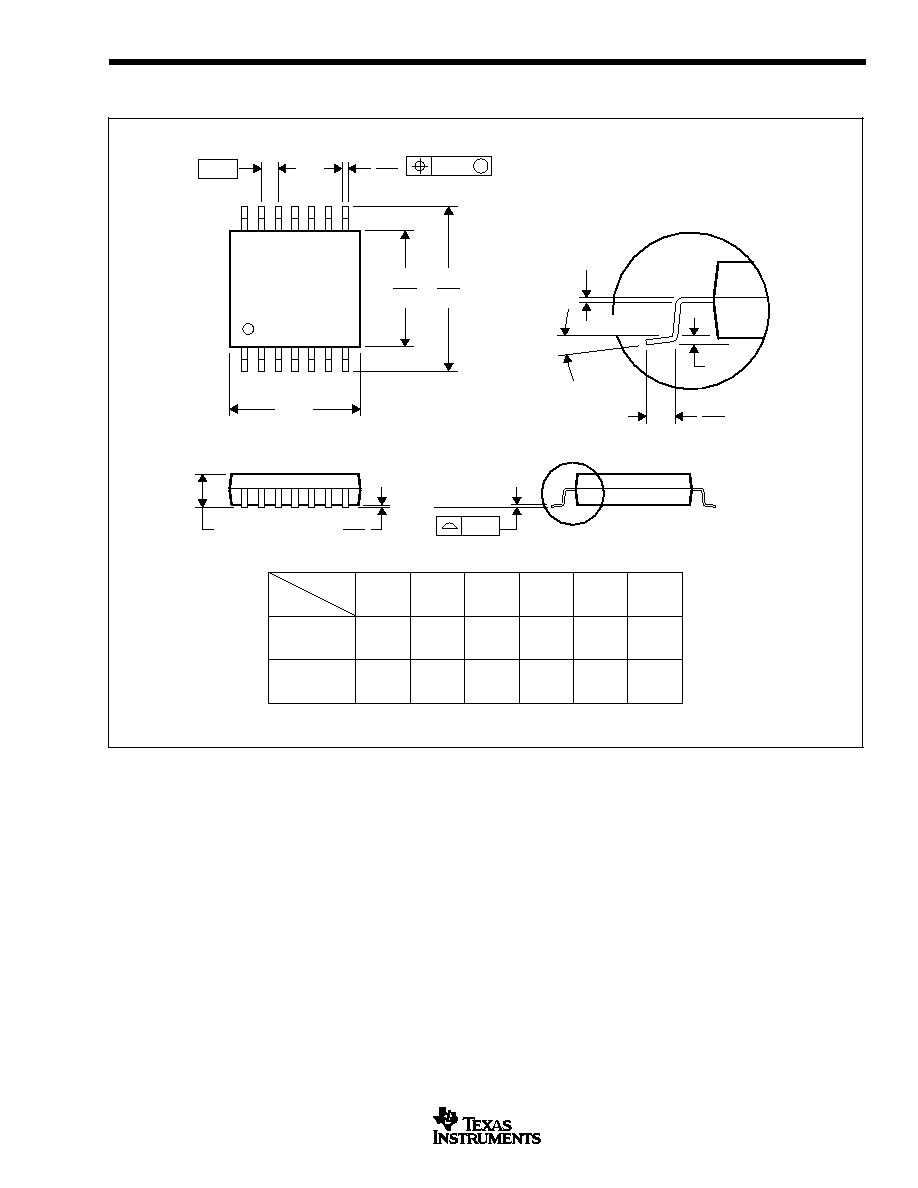
PACKAGE DRAWINGS (Cont.)
D (R-PDSO-G**)
PLASTIC SMALL-OUTLINE PACKAGE
8 PINS SHOWN
8
0.197
(5,00)
A MAX
A MIN
(4,80)
0.189
0.337
(8,55)
(8,75)
0.344
14
0.386
(9,80)
(10,00)
0.394
16
DIM
PINS **
4040047/E 09/01
0.069 (1,75) MAX
Seating Plane
0.004 (0,10)
0.010 (0,25)
0.010 (0,25)
0.016 (0,40)
0.044 (1,12)
0.244 (6,20)
0.228 (5,80)
0.020 (0,51)
0.014 (0,35)
1
4
8
5
0.150 (3,81)
0.157 (4,00)
0.008 (0,20) NOM
0
∞
≠ 8
∞
Gage Plane
A
0.004 (0,10)
0.010 (0,25)
0.050 (1,27)
NOTES: A. All linear dimensions are in inches (millimeters).
B. This drawing is subject to change without notice.
C. Body dimensions do not include mold flash or protrusion, not to exceed 0.006 (0,15).
D. Falls within JEDEC MS-012

OPA347, 2347, 4347
16
SBOS167C
www.ti.com
DCK (R-PDSO-G5)
PLASTIC SMALL-OUTLINE
0,10
M
0,10
0,65
0
∞
≠8
∞
0,15
0,46
0,26
Gage Plane
0,13 NOM
4093553/B 06/99
0,15
0,30
1,40
1,10
2,30
1,90
4
5
2,15
1,85
1
3
1,10
0,80
0,10
0,00
Seating Plane
NOTES: A. All linear dimensions are in millimeters.
B. This drawing is subject to change without notice.
C. Body dimensions do not include mold flash or protrusion.
D. Falls within JEDEC MO-203
PACKAGE DRAWINGS (Cont.)
OPA347, 2347, 4347
17
SBOS167C
www.ti.com
DCN (R-PDSO-G8)
PLASTIC SMALL-OUTLINE
C
4202106/A 03/01
3,00
2,80
3,00
2,60
1,50
1,75
Area
0,28
0,45
0
∞
≠10
∞
0,09
0,20
1,30
0,90
0,10
0,60
Index
0,00
0,15
≠A≠
0,65
0,90
1,45
1,95 REF
NOTES: A. All linear dimensions are in millimeters.
B. This drawing is subject to change without notice.
C. Foot length measured reference to flat foot surface
parallel to Datum A.
D. Package outline exclusive of mold flash, metal burr and
dambar protrusion/intrusion.
E. Package outline inclusive of solder plating.
F. A visual index feature must be located within the
cross-hatched area.
PACKAGE DRAWINGS (Cont.)

OPA347, 2347, 4347
18
SBOS167C
www.ti.com
PACKAGE DRAWINGS (Cont.)
OPA347, 2347, 4347
19
SBOS167C
www.ti.com
PW (R-PDSO-G**)
PLASTIC SMALL-OUTLINE PACKAGE
14 PINS SHOWN
0,65
M
0,10
0,10
0,25
0,50
0,75
0,15 NOM
Gage Plane
28
9,80
9,60
24
7,90
7,70
20
16
6,60
6,40
4040064/F 01/97
0,30
6,60
6,20
8
0,19
4,30
4,50
7
0,15
14
A
1
1,20 MAX
14
5,10
4,90
8
3,10
2,90
A MAX
A MIN
DIM
PINS **
0,05
4,90
5,10
Seating Plane
0
∞
≠ 8
∞
NOTES: A. All linear dimensions are in millimeters.
B. This drawing is subject to change without notice.
C. Body dimensions do not include mold flash or protrusion not to exceed 0,15.
D. Falls within JEDEC MO-153
PACKAGE DRAWINGS (Cont.)

PACKAGING INFORMATION
ORDERABLE DEVICE
STATUS(1)
PACKAGE TYPE
PACKAGE DRAWING
PINS
PACKAGE QTY
OPA2347EA/250
ACTIVE
SSOP
DCN
8
250
OPA2347EA/3K
ACTIVE
SSOP
DCN
8
3000
OPA2347UA
ACTIVE
SOIC
D
8
100
OPA2347UA/2K5
ACTIVE
SOIC
D
8
2500
OPA2347YEDR
ACTIVE
8
2500
OPA2347YEDT
ACTIVE
8
250
OPA347NA/250
ACTIVE
SOP
DBV
5
250
OPA347NA/3K
ACTIVE
SOP
DBV
5
3000
OPA347PA
ACTIVE
PDIP
P
8
50
OPA347SA/250
ACTIVE
SOP
DCK
5
250
OPA347SA/3K
ACTIVE
SOP
DCK
5
3000
OPA347UA
ACTIVE
SOIC
D
8
100
OPA347UA/2K5
ACTIVE
SOIC
D
8
2500
OPA4347EA/250
ACTIVE
TSSOP
PW
14
250
OPA4347EA/2K5
ACTIVE
TSSOP
PW
14
2500
OPA4347UA
ACTIVE
SOIC
D
14
58
OPA4347UA/2K5
ACTIVE
SOIC
D
14
2500
(1) The marketing status values are defined as follows:
ACTIVE: Product device recommended for new designs.
LIFEBUY: TI has announced that the device will be discontinued, and a lifetime-buy period is in effect.
NRND: Not recommended for new designs. Device is in production to support existing customers, but TI does not recommend using this part in
a new design.
PREVIEW: Device has been announced but is not in production. Samples may or may not be available.
OBSOLETE: TI has discontinued the production of the device.
PACKAGE OPTION ADDENDUM
www.ti.com
3-Oct-2003

IMPORTANT NOTICE
Texas Instruments Incorporated and its subsidiaries (TI) reserve the right to make corrections, modifications,
enhancements, improvements, and other changes to its products and services at any time and to discontinue
any product or service without notice. Customers should obtain the latest relevant information before placing
orders and should verify that such information is current and complete. All products are sold subject to TI's terms
and conditions of sale supplied at the time of order acknowledgment.
TI warrants performance of its hardware products to the specifications applicable at the time of sale in
accordance with TI's standard warranty. Testing and other quality control techniques are used to the extent TI
deems necessary to support this warranty. Except where mandated by government requirements, testing of all
parameters of each product is not necessarily performed.
TI assumes no liability for applications assistance or customer product design. Customers are responsible for
their products and applications using TI components. To minimize the risks associated with customer products
and applications, customers should provide adequate design and operating safeguards.
TI does not warrant or represent that any license, either express or implied, is granted under any TI patent right,
copyright, mask work right, or other TI intellectual property right relating to any combination, machine, or process
in which TI products or services are used. Information published by TI regarding third-party products or services
does not constitute a license from TI to use such products or services or a warranty or endorsement thereof.
Use of such information may require a license from a third party under the patents or other intellectual property
of the third party, or a license from TI under the patents or other intellectual property of TI.
Reproduction of information in TI data books or data sheets is permissible only if reproduction is without
alteration and is accompanied by all associated warranties, conditions, limitations, and notices. Reproduction
of this information with alteration is an unfair and deceptive business practice. TI is not responsible or liable for
such altered documentation.
Resale of TI products or services with statements different from or beyond the parameters stated by TI for that
product or service voids all express and any implied warranties for the associated TI product or service and
is an unfair and deceptive business practice. TI is not responsible or liable for any such statements.
Following are URLs where you can obtain information on other Texas Instruments products and application
solutions:
Products
Applications
Amplifiers
amplifier.ti.com
Audio
www.ti.com/audio
Data Converters
dataconverter.ti.com
Automotive
www.ti.com/automotive
DSP
dsp.ti.com
Broadband
www.ti.com/broadband
Interface
interface.ti.com
Digital Control
www.ti.com/digitalcontrol
Logic
logic.ti.com
Military
www.ti.com/military
Power Mgmt
power.ti.com
Optical Networking
www.ti.com/opticalnetwork
Microcontrollers
microcontroller.ti.com
Security
www.ti.com/security
Telephony
www.ti.com/telephony
Video & Imaging
www.ti.com/video
Wireless
www.ti.com/wireless
Mailing Address:
Texas Instruments
Post Office Box 655303 Dallas, Texas 75265
Copyright
2003, Texas Instruments Incorporated