
OPA244
OPA2244
OPA4244
Æ
© 1999 Burr-Brown Corporation
PDS-1437C
Printed in U.S.A. December, 1999
FEATURES
q
Micro
SIZE PACKAGES
OPA244 (Single): SOT-23-5
OPA2244 (Dual): MSOP-8
OPA4244 (Quad): TSSOP-14
q
Micro
POWER: I
Q
= 50
µ
A/channel
q
SINGLE SUPPLY OPERATION
q
WIDE BANDWIDTH: 430kHz
q
WIDE SUPPLY RANGE:
Single Supply: 2.2V to 36V
Dual Supply:
±
1.1V to
±
18V
DESCRIPTION
The OPA244 (single), OPA2244 (dual), and OPA4244 (quad)
op amps are designed for very low quiescent current
(50
µ
A/channel), yet achieve excellent bandwidth. Ideal for
battery powered and portable instrumentation, all versions are
offered in micro packages for space-limited applications.
The dual and quad versions feature completely independent
circuitry for lowest crosstalk and freedom from interaction, even
when overdriven or overloaded.
The OPA244 series is easy to use and free from phase
inversion and overload problems found in some other op amps.
These amplifiers are stable in unity gain and excellent perfor-
mance is maintained as they swing to their specified limits.
They can be operated from single (+2.2V to +36V) or dual
supplies (
±
1.1V to
±
18V). The input common-mode voltage
range includes ground--ideal for many single supply applica-
tions. All versions have similar performance. However, there
are some differences, such as common-mode rejection. All
versions are interchangeable in most applications.
All versions are offered in miniature, surface-mount packages.
OPA244 (single version) comes in the tiny 5-lead SOT-23-5
surface mount, SO-8 surface mount, and 8-pin DIP. OPA2244
(dual version) is available in the MSOP-8 surface mount,
SO-8 surface-mount, and 8-pin DIP. The OPA4244 (quad)
comes in the TSSOP-14 surface mount. They are fully specified
from ≠40
∞
C to +85
∞
C and operate from ≠55
∞
C to +125
∞
C.
A SPICE Macromodel is available for design analysis.
Micro
Power, Single-Supply
OPERATIONAL AMPLIFIERS
Micro
Amplifier
TM
Series
APPLICATIONS
q
BATTERY POWERED SYSTEMS
q
PORTABLE EQUIPMENT
q
PCMCIA CARDS
q
BATTERY PACKS AND POWER SUPPLIES
q
CONSUMER PRODUCTS
1
2
3
4
8
7
6
5
V+
Out B
≠In B
+In B
Out A
≠In A
+In A
V≠
OPA2244
8-Pin DIP, SO-8, MSOP-8
A
B
1
2
3
5
4
V+
≠In
Out
V≠
+In
OPA244
SOT-23-5
1
2
3
4
8
7
6
5
NC
V+
Output
NC
NC
≠In
+In
V≠
OPA244
8-Pin DIP, SO-8
Æ
OPA4244
OPA244
OPA244
OPA2244
OPA2244
International Airport Industrial Park ∑ Mailing Address: PO Box 11400, Tucson, AZ 85734 ∑ Street Address: 6730 S. Tucson Blvd., Tucson, AZ 85706 ∑ Tel: (520) 746-1111
Twx: 910-952-1111 ∑ Internet: http://www.burr-brown.com/ ∑ Cable: BBRCORP ∑ Telex: 066-6491 ∑ FAX: (520) 889-1510 ∑ Immediate Product Info: (800) 548-6132
1
2
3
4
5
6
7
14
13
12
11
10
9
8
Output D
≠Input D
+Input D
≠V
+Input C
≠Input C
Output C
Output A
≠Input A
+Input A
+V
+Input B
≠Input B
Output B
OPA4244
TSSOP-14
SBOS088

2
Æ
OPA244, 2244, 4244
The information provided herein is believed to be reliable; however, BURR-BROWN assumes no responsibility for inaccuracies or omissions. BURR-BROWN assumes
no responsibility for the use of this information, and all use of such information shall be entirely at the user's own risk. Prices and specifications are subject to change
without notice. No patent rights or licenses to any of the circuits described herein are implied or granted to any third party. BURR-BROWN does not authorize or warrant
any BURR-BROWN product for use in life support devices and/or systems.
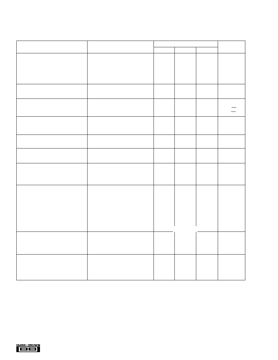
OPA244NA, PA, UA
PARAMETER
CONDITION
MIN
TYP
(1)
MAX
UNITS
OFFSET VOLTAGE
Input Offset Voltage
V
OS
V
S
=
±
7.5V, V
CM
= 0
±
0.7
±
1.5
mV
T
A
= ≠40
∞
C to 85
∞
C
±
2
mV
vs Temperature
dV
OS
/dT
T
A
= ≠40
∞
C to 85
∞
C
±
4
µ
V/
∞
C
vs Power Supply
PSRR
V
S
= +2.6V to +36V
5
50
µ
V/V
T
A
= ≠40
∞
C to 85
∞
C
V
S
= +2.6V to +36V
50
µ
V/V
INPUT BIAS CURRENT
Input Bias Current
I
B
V
CM
= V
S
/2
≠10
≠25
nA
Input Offset Current
I
OS
V
CM
= V
S
/2
±
1
±
10
nA
NOISE
Input Voltage Noise, f = 0.1kHz to 10kHz
0.4
µ
Vp-p
Input Voltage Noise Density, f = 1kHz
e
n
22
nV/
Hz
Current Noise Density, f = 1kHz
i
n
40
fA/
Hz
INPUT VOLTAGE RANGE
Common-Mode Voltage Range
V
CM
0
(V+) ≠ 0.9
V
Common-Mode Rejection
CMRR
V
S
=
±
18V, V
CM
= ≠18V to +17.1V
84
98
dB
T
A
= ≠40
∞
C to 85
∞
C
V
S
=
±
18V, V
CM
= ≠18V to +17.1V
84
dB
INPUT IMPEDANCE
Differential
10
6
|| 2
|| pF
Common-Mode
10
9
|| 2
|| pF
OPEN-LOOP GAIN
Open-Loop Voltage Gain
A
OL
V
O
= 0.5V to (V+) ≠ 0.9
86
106
dB
T
A
= ≠40
∞
C to 85
∞
C
V
O
= 0.5V to (V+) ≠ 0.9
86
dB
FREQUENCY RESPONSE
Gain-Bandwidth Product
GBW
430
kHz
Slew Rate
SR
G = 1
≠0.1/+0.16
V/
µ
s
Settling Time 0.01%
10V Step
150
µ
s
Overload Recovery Time
V
IN
∑ Gain = V
S
8
µ
s
OUTPUT
Voltage Output, Positive
V
O
A
OL
80dB, R
L
= 20k
to V
S
/2
(V+) ≠ 0.9
(V+) ≠ 0.75
V
T
A
= ≠40
∞
C to 85
∞
C
A
OL
80dB, R
L
= 20k
to V
S
/2
(V+) ≠ 0.9
(V+) ≠ 0.75
V
Voltage Output, Negative
A
OL
80dB, R
L
= 20k
to V
S
/2
0.5
0.2
V
T
A
= ≠40
∞
C to 85
∞
C
A
OL
80dB, R
L
= 20k
to V
S
/2
0.5
0.2
V
Voltage Output, Positive
A
OL
80dB, R
L
= 20k
to Ground
(V+) ≠ 0.75
V
T
A
= ≠40
∞
C to 85
∞
C
A
OL
80dB, R
L
= 20k
to Ground
(V+) ≠ 0.75
V
Voltage Output, Negative
A
OL
80dB, R
L
= 20k
to Ground
0.1
V
T
A
= ≠40
∞
C to 85
∞
C
A
OL
80dB, R
L
= 20k
to Ground
0.1
V
Short-Circuit Current
I
SC
≠25 /+12
mA
Capacitive Load Drive
C
LOAD
See Typical Curve
POWER SUPPLY
Specified Voltage Range
V
S
T
A
= ≠40
∞
C to 85
∞
C
+2.6
+36
V
Minimum Operating Voltage
+2.2
V
Quiescent Current
I
Q
I
O
= 0
50
60
µ
A
T
A
= ≠40
∞
C to 85
∞
C
I
O
= 0
70
µ
A
TEMPERATURE RANGE
Specified Range
≠40
85
∞
C
Operating Range
≠55
125
∞
C
Storage Range
≠65
150
∞
C
Thermal Resistance
JA
SOT-23-5 Surface-Mount
200
∞
C/W
SO-8 Surface-Mount
150
∞
C/W
8-Pin DIP
100
∞
C/W
NOTE: (1) V
S
= +15V.
SPECIFICATIONS: V
S
= +2.6V to +36V
Boldface limits apply over the specified temperature range, T
A
= ≠40
∞
C to +85
∞
C
At T
A
= +25
∞
C, R
L
= 20k
connected to ground, unless otherwise noted.

3
OPA244, 2244, 4244
Æ
OPA2244EA, PA, UA
PARAMETER
CONDITION
MIN
TYP
(1)
MAX
UNITS
OFFSET VOLTAGE
Input Offset Voltage
V
OS
V
S
=
±
7.5V, V
CM
= 0
±
0.7
±
1.5
mV
T
A
= ≠40
∞
C to 85
∞
C
±
2
mV
vs Temperature
dV
OS
/dT
T
A
= ≠40
∞
C to 85
∞
C
±
4
µ
V/
∞
C
vs Power Supply
PSRR
V
S
= +2.6V to +36V
5
50
µ
V/V
T
A
= ≠40
∞
C to 85
∞
C
V
S
= +2.6V to +36V
50
µ
V/V
Channel Separation
140
dB
INPUT BIAS CURRENT
Input Bias Current
I
B
V
CM
= V
S
/2
≠10
≠25
nA
Input Offset Current
I
OS
V
CM
= V
S
/2
±
1
±
10
nA
NOISE
Input Voltage Noise, f = 0.1kHz to 10kHz
0.4
µ
Vp-p
Input Voltage Noise Density, f = 1kHz
e
n
22
nV/
Hz
Current Noise Density, f = 1kHz
i
n
40
fA/
Hz
INPUT VOLTAGE RANGE
Common-Mode Voltage Range
V
CM
0
(V+) ≠ 0.9
V
Common-Mode Rejection
CMRR
V
S
=
±
18V, V
CM
= ≠18V to +17.1V
72
98
dB
T
A
= ≠40
∞
C to 85
∞
C
V
S
=
±
18V, V
CM
= ≠18V to +17.1V
72
dB
INPUT IMPEDANCE
Differential
10
6
|| 2
|| pF
Common-Mode
10
9
|| 2
|| pF
OPEN-LOOP GAIN
Open-Loop Voltage Gain
A
OL
V
O
= 0.5V to (V+) ≠ 0.9
86
106
dB
T
A
= ≠40
∞
C to 85
∞
C
V
O
= 0.5V to (V+) ≠ 0.9
86
dB
FREQUENCY RESPONSE
Gain-Bandwidth Product
GBW
430
kHz
Slew Rate
SR
G = 1
≠0.1/+0.16
V/
µ
s
Settling Time 0.01%
10V Step
150
µ
s
Overload Recovery Time
V
IN
∑ Gain = V
S
8
µ
s
OUTPUT
Voltage Output, Positive
V
O
A
OL
80dB, R
L
= 20k
to V
S
/2
(V+) ≠ 0.9
(V+) ≠ 0.75
V
T
A
= ≠40
∞
C to 85
∞
C
A
OL
80dB, R
L
= 20k
to V
S
/2
(V+) ≠ 0.9
(V+) ≠ 0.75
V
Voltage Output, Negative
A
OL
80dB, R
L
= 20k
to V
S
/2
0.5
0.2
V
T
A
= ≠40
∞
C to 85
∞
C
A
OL
80dB, R
L
= 20k
to V
S
/2
0.5
0.2
V
Voltage Output, Positive
A
OL
80dB, R
L
= 20k
to Ground
(V+) ≠ 0.75
V
T
A
= ≠40
∞
C to 85
∞
C
A
OL
80dB, R
L
= 20k
to Ground
(V+) ≠ 0.75
V
Voltage Output, Negative
A
OL
80dB, R
L
= 20k
to Ground
0.1
V
T
A
= ≠40
∞
C to 85
∞
C
A
OL
80dB, R
L
= 20k
to Ground
0.1
V
Short-Circuit Current
I
SC
≠25 /+12
mA
Capacitive Load Drive
C
LOAD
See Typical Curve
POWER SUPPLY
Specified Voltage Range
V
S
T
A
= ≠40
∞
C to 85
∞
C
+2.6
+36
V
Minimum Operating Voltage
+2.2
V
Quiescent Current (per amplifier)
I
Q
I
O
= 0
40
50
µ
A
T
A
= ≠40
∞
C to 85
∞
C
I
O
= 0
63
µ
A
TEMPERATURE RANGE
Specified Range
≠40
85
∞
C
Operating Range
≠55
125
∞
C
Storage Range
≠65
150
∞
C
Thermal Resistance
JA
MSOP-8 Surface-Mount
200
∞
C/W
SO-8 Surface-Mount
150
∞
C/W
8-Pin DIP
100
∞
C/W
NOTE: (1) V
S
= +15V.
SPECIFICATIONS: V
S
= +2.6V to +36V
Boldface limits apply over the specified temperature range, T
A
= ≠40
∞
C to +85
∞
C
At T
A
= +25
∞
C, R
L
= 20k
connected to ground, unless otherwise noted.
4
Æ
OPA244, 2244, 4244
OPA4244EA
PARAMETER
CONDITION
MIN
TYP
(1)
MAX
UNITS
OFFSET VOLTAGE
Input Offset Voltage
V
OS
V
S
=
±
7.5V, V
CM
= 0
±
0.7
±
1.5
mV
T
A
= ≠40
∞
C to 85
∞
C
±
2
mV
vs Temperature
dV
OS
/dT
T
A
= ≠40
∞
C to 85
∞
C
±
4
µ
V/
∞
C
vs Power Supply
PSRR
V
S
= +2.6V to +36V
5
50
µ
V/V
T
A
= ≠40
∞
C to 85
∞
C
V
S
= +2.6V to +36V
50
µ
V/V
Channel Separation
140
dB
INPUT BIAS CURRENT
Input Bias Current
I
B
V
CM
= V
S
/2
≠10
≠25
nA
Input Offset Current
I
OS
V
CM
= V
S
/2
±
1
±
10
nA
NOISE
Input Voltage Noise, f = 0.1kHz to 10kHz
0.4
µ
Vp-p
Input Voltage Noise Density, f = 1kHz
e
n
22
nV/
Hz
Current Noise Density, f = 1kHz
i
n
40
fA/
Hz
INPUT VOLTAGE RANGE
Common-Mode Voltage Range
V
CM
0
(V+) ≠ 0.9
V
Common-Mode Rejection
CMRR
V
S
=
±
18V, V
CM
= ≠18V to +17.1V
82
104
dB
T
A
= ≠40
∞
C to 85
∞
C
V
S
=
±
18V, V
CM
= ≠18V to +17.1V
82
dB
INPUT IMPEDANCE
Differential
10
6
|| 2
|| pF
Common-Mode
10
9
|| 2
|| pF
OPEN-LOOP GAIN
Open-Loop Voltage Gain
A
OL
V
O
= 0.5V to (V+) ≠ 0.9
86
106
dB
T
A
= ≠40
∞
C to 85
∞
C
V
O
= 0.5V to (V+) ≠ 0.9
86
dB
FREQUENCY RESPONSE
Gain-Bandwidth Product
GBW
430
kHz
Slew Rate
SR
G = 1
≠0.1/+0.16
V/
µ
s
Settling Time 0.01%
10V Step
150
µ
s
Overload Recovery Time
V
IN
∑ Gain = V
S
8
µ
s
OUTPUT
Voltage Output, Positive
V
O
A
OL
80dB, R
L
= 20k
to V
S
/2
(V+) ≠ 0.9
(V+) ≠ 0.75
V
T
A
= ≠40
∞
C to 85
∞
C
A
OL
80dB, R
L
= 20k
to V
S
/2
(V+) ≠ 0.9
(V+) ≠ 0.75
V
Voltage Output, Negative
A
OL
80dB, R
L
= 20k
to V
S
/2
0.5
0.2
V
T
A
= ≠40
∞
C to 85
∞
C
A
OL
80dB, R
L
= 20k
to V
S
/2
0.5
0.2
V
Voltage Output, Positive
A
OL
80dB, R
L
= 20k
to Ground
(V+) ≠ 0.75
V
T
A
= ≠40
∞
C to 85
∞
C
A
OL
80dB, R
L
= 20k
to Ground
(V+) ≠ 0.75
V
Voltage Output, Negative
A
OL
80dB, R
L
= 20k
to Ground
0.1
V
T
A
= ≠40
∞
C to 85
∞
C
A
OL
80dB, R
L
= 20k
to Ground
0.1
V
Short-Circuit Current
I
SC
≠25 /+12
mA
Capacitive Load Drive
C
LOAD
See Typical Curve
POWER SUPPLY
Specified Voltage Range
V
S
T
A
= ≠40
∞
C to 85
∞
C
+2.6
+36
V
Minimum Operating Voltage
+2.2
V
Quiescent Current (per amplifier)
I
Q
I
O
= 0
40
60
µ
A
T
A
= ≠40
∞
C to 85
∞
C
I
O
= 0
70
µ
A
TEMPERATURE RANGE
Specified Range
≠40
85
∞
C
Operating Range
≠55
125
∞
C
Storage Range
≠65
150
∞
C
Thermal Resistance
JA
TSSOP-14 Surface Mount
100
∞
C/W
NOTE: (1) V
S
= +15V.
SPECIFICATIONS: V
S
= +2.6V to +36V
Boldface limits apply over the specified temperature range, T
A
= ≠40
∞
C to +85
∞
C
At T
A
= +25
∞
C, R
L
= 20k
connected to ground, unless otherwise noted.
5
OPA244, 2244, 4244
Æ
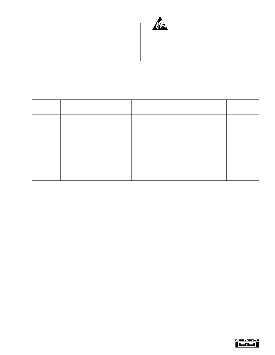
PACKAGE
SPECIFIED
DRAWING
TEMPERATURE
PACKAGE
ORDERING
TRANSPORT
PRODUCT
PACKAGE
NUMBER
RANGE
MARKING
NUMBER
(1)
MEDIA
Single
OPA244NA
SOT-23-5 Surface-Mount
331
≠40
∞
C to +85
∞
C
A44
OPA244NA/250
Tape and Reel
"
"
"
"
"
OPA244NA/3K
Tape and Reel
OPA244PA
8-Pin DIP
006
≠40
∞
C to +85
∞
C
OPA244PA
OPA244PA
Rails
OPA244UA
SO-8 Surface-Mount
182
≠40
∞
C to +85
∞
C
OPA244UA
OPA244UA
Rails
"
"
"
"
"
OPA244UA/2K5
Tape and Reel
Dual
OPA2244EA
MSOP-8 Surface-Mount
337
≠40
∞
C to +85
∞
C
A44
OPA2244EA/250
Tape and Reel
"
"
"
"
"
OPA2244EA/2K5
Tape and Reel
OPA2244PA
8-Pin DIP
006
≠40
∞
C to +85
∞
C
OPA2244PA
OPA2244PA
Rails
OPA2244UA
SO-8 Surface-Mount
182
≠40
∞
C to +85
∞
C
OPA2244UA
OPA2244UA
Rails
"
"
"
"
"
OPA2244UA/2K5
Tape and Reel
Quad
OPA4244EA
TSSOP-14 Surface-Mount
357
≠40
∞
C to +85
∞
C
OPA4244EA
OPA4244EA/250
Tape and Reel
"
"
"
"
"
OPA4244EA/2K5
Tape and Reel
NOTE: (1) Products followed by a slash (/) are only available in Tape and Reel in the quantities indicated (e.g., /250 indicates 250 devices per reel). Ordering 3000
pieces of "OPA244NA/3K" will get a single 3000 piece Tape and Reel.
ELECTROSTATIC
DISCHARGE SENSITIVITY
This integrated circuit can be damaged by ESD. Burr-Brown
recommends that all integrated circuits be handled with
appropriate precautions. Failure to observe proper handling
and installation procedures can cause damage.
ESD damage can range from subtle performance degrada-
tion to complete device failure. Precision integrated circuits
may be more susceptible to damage because very small
parametric changes could cause the device not to meet its
published specifications.
Supply Voltage, V+ to V≠ .................................................................... 36V
Input Voltage Range
(2)
................................... (V≠) ≠ 0.3V to (V+) + 0.3V
Input Current
(2)
................................................................................. 10mA
Output Short-Circuit
(3)
.............................................................. Continuous
Operating Temperature .................................................. ≠55
∞
C to +125
∞
C
Storage Temperature ..................................................... ≠65
∞
C to +150
∞
C
Junction Temperature ...................................................................... 150
∞
C
Lead Temperature (soldering, 10s) ................................................. 300
∞
C
ESD Capability ................................................................................ 2000V
NOTES: (1) Stresses above these ratings may cause permanent damage.
Exposure to absolute maximum conditions for extended periods may de-
grade device reliability. (2) Inputs are diode-clamped to the supply rails and
should be current-limited to 10mA or less if input voltages can exceed rails
by more than 0.3V. (3) Short-circuit to ground, one amplifier per package.
ABSOLUTE MAXIMUM RATINGS
(1)
PACKAGE /ORDERING INFORMATION

6
Æ
OPA244, 2244, 4244
TYPICAL PERFORMANCE CURVES
At T
A
= 25
∞
C, V
S
= +15V, and R
L
= 20k
connected to Ground, unless otherwise noted.
180
160
140
120
100
80
60
40
20
0
≠20
OPEN-LOOP GAIN AND PHASE vs FREQUENCY
1
Frequency (Hz)
10
100
1k
10k
100k
1M
0
≠20
≠40
≠60
≠80
≠100
≠120
≠140
≠160
≠180
≠200
A
OL
(dB)
Phase(
∞
)
All Models
Gain
Phase
160
150
140
130
120
110
100
90
80
70
60
CHANNEL SEPARATION
1
10
100
1k
10k
100k
Separation (dB)
OPA4244
Frequency (Hz)
OPA2244
OPA244
Frequency (Hz)
PSRR, CMRR (dB)
110
100
90
80
70
60
50
40
30
10
100
1k
10k
100k
1M
PSRR
OPA2244
OPA244
CMRR
120
110
100
90
80
70
60
1
10
100
OPEN-LOOP GAIN vs LOAD RESISTANCE
Gain(dB)
Load (k
)
V
O
=
±
5V
OUTPUT VOLTAGE SWING vs OUTPUT CURRENT
15
14
13
12
11
10
≠10
≠11
≠12
≠13
≠14
≠15
0
±
2
±
4
±
6
±
8
±
10
±
14
±
12
Output Current (mA)
Output Voltage Swing (V)
25
∞
C
125
∞
C
≠55
∞
C
≠55
∞
C
125
∞
C
25
∞
C
R
L
to V
S
/2
POWER SUPPLY AND COMMON-MODE REJECTION vs FREQUENCY
1
10
100
1k
10k
100k
1M
Frequency (Hz)
120
110
100
90
80
70
60
50
40
30
PSRR, CMRR (dB)
OPA4244
CMRR
PSRR
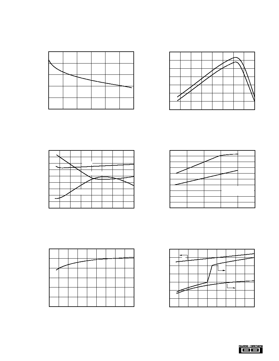
7
OPA244, 2244, 4244
Æ
TYPICAL PERFORMANCE CURVES
(Cont.)
At T
A
= 25
∞
C, V
S
= +15V, and R
L
= 20k
connected to Ground, unless otherwise noted.
INPUT BIAS CURRENT
vs INPUT COMMON-MODE VOLTAGE
Common-Mode Voltage (V)
Bias Current (nA)
≠12
≠10
≠8
≠6
≠4
≠2
≠15
≠10
≠5
0
5
10
15
52
48
44
40
36
32
28
24
Quiescent Current (
µ
A)
0
4
8
12
16
20
24
28
32
36
35
30
25
20
15
10
5
0
Short-Circuit Current (mA)
Supply Voltage (V)
QUIESCENT CURRENT AND SHORT-CIRCUIT
vs SUPPLY VOLTAGE
+I
SC
≠I
SC
I
Q
120
100
80
60
40
20
0
COMMON-MODE REJECTION
vs SUPPY VOLTAGE
0
4
8
12
16
20
24
28
32
36
Suppy Voltage (V)
CMRR (dB)
0.20
0.18
0.16
0.14
0.12
0.10
0.08
0.06
0.04
0.02
0.00
≠75
≠25
25
75
125
175
Temperature (
∞
C)
SLEW RATE vs TEMPERATURE
V
S
=
±
7.5, R
L
= 20k
,
C
L
= 100pF, Gain = +1
+SR
≠SR
Slew Rate (V/
µ
s)
125
120
115
110
105
100
95
90
85
80
≠75
≠50
≠25
0
25
50
75
100
125
A
OL
, CMRR, PSRR vs TEMPERATURE
Temperature(
∞
C)
PSRR
CMRR
A
OL
INPUT BIAS CURRENT vs TEMPERATURE
Temperature (
∞
C)
Bias Current (nA)
≠12
≠11
≠10
≠9
≠8
≠7
≠6
≠5
≠75
≠50
≠25
0
25
50
75
100
125
≠I
B
+I
B

8
Æ
OPA244, 2244, 4244
TYPICAL PERFORMANCE CURVES
(Cont.)
At T
A
= 25
∞
C, V
S
= +15V, and R
L
= 20k
connected to Ground, unless otherwise noted.
70%
60%
50%
40%
30%
20%
10%
0%
10
100
1k
10k
Load Capacitance (pF)
Overshoot (%)
G = +1, R
L
=
G = +1, R
L
= 20k
G = +2, R
L
= 20k
G = +3, R
L
= 20k
OPA4244
Load Capacitance (pF)
Overshoot (%)
60
50
40
30
20
10
0
100
1k
10k
G = ≠1
G = ≠2
G = +3
G = +1
OPA2244
OPA244
40
35
30
25
20
15
10
5
0
100
1k
10k
100k
1M
Frequency(Hz)
Output V
oltage (Vp-p)
MAXIMUM OUTPUT VOLTAGE vs FREQUENCY
V
S
= 2.7V
V
S
=15V
V
S
= 36V
INPUT VOLTAGE AND CURRENT NOISE
SPECTRAL DENSITY vs FREQUENCY
Frequency (Hz)
Voltage Noise (nV
Hz)
1000
100
10
1
1
10
100
1k
10k
100k
Current Noise (fA
Hz)
1000
100
10
1
Voltage Noise
Current Noise
Temperature (
∞
C)
Quiescent Current (
µ
A)
65
60
55
50
45
40
35
30
25
Short-Circuit Current (mA)
±
40
±
35
±
30
±
25
±
20
±
15
±
10
±
5
0
≠75
≠50
≠25
0
25
50
75
100
125
≠I
SC
+I
SC
I
Q
OPA2244
OPA244
QUIESCENT AND SHORT-CIRCUIT CURRENT vs TEMPERATURE
60
55
50
45
40
35
30
20
≠30
≠25
≠20
≠15
+15
+10
+5
0
Short-Circuit Current (mA)
Quiescent Current (
µ
A)
≠75
≠50
≠25
0
25
50
75
100
125
Temperature (
∞
C)
≠I
SC
+I
SC
I
Q
OPA4244
SMALL SIGNAL OVERSHOOT vs LOAD CAPACITANCE

9
OPA244, 2244, 4244
Æ
TYPICAL PERFORMANCE CURVES
(Cont.)
At T
A
= 25
∞
C, V
S
= +15V, and R
L
= 20k
connected to Ground, unless otherwise noted.
50mV/div
10
µ
s/div
OPA4244
2V/div
50
µ
s/div
OPA4244
LARGE-SIGNAL STEP RESPONSE, G = 1, C
L
= 100pF
SMALL-SIGNAL STEP RESPONSE, G = 1, C
L
= 100pF
OPA244
OPA2244
OPA244
OPA2244
25
µ
s/div
2V/div
10
µ
s/div
50mV/div
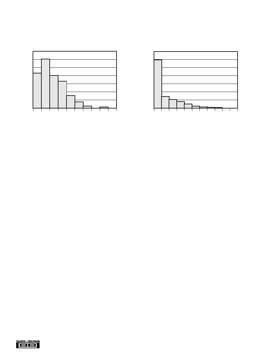
OFFSET VOLTAGE PRODUCTION DISTRIBUTION
Percent of Amplifiers (%)
Offset Voltage (
µ
V)
≠1500
≠1300
≠1100
≠900
≠700
≠500
≠300
≠100
0
100
300
500
700
900
1100
1300
1500
12
10
8
6
4
2
0
OPA2244
OPA244
Percent of Amplifiers (%)
Offset Voltage (
µ
V)
≠1500
≠1200
≠900
≠600
≠300
0
300
600
900
1200
1500
1800
30
25
20
15
10
5
0
OPA4244
10
Æ
OPA244, 2244, 4244
TYPICAL PERFORMANCE CURVES
(Cont.)
At T
A
= 25
∞
C, V
S
= +15V, and R
L
= 20k
connected to Ground, unless otherwise noted.
Percent of Amplifiers (%)
V
OS
Drift (
µ
V/
∞
C)
0
0.5
1
1.5
2
2.5
3
3.5
4
4.5
5.0
5.5
70
60
50
40
30
20
10
0
OPA4244
Percent of Amplifiers (%)
V
OS
Drift (
µ
V/
∞
C)
0
1
2
3
4
5
6
7
8
9
10
35
30
25
20
15
10
5
0
OPA2244
OPA244
OFFSET VOLTAGE PRODUCTION DISTRIBUTION

11
OPA244, 2244, 4244
Æ
APPLICATIONS INFORMATION
The OPA244 is unity-gain stable and suitable for a wide
range of general purpose applications. Power supply pins
should be bypassed with 0.01
µ
F ceramic capacitors.
OPERATING VOLTAGE
The OPA244 can operate from single supply (+2.2V to
+36V) or dual supplies (
±
1.1 to
±
18V) with excellent
performance. Unlike most op amps which are specified at
only one supply voltage, the OPA244 is specified for real
world applications; a single set of specifications applies
throughout the +2.6V to +36V (
±
1.3 to
±
18V) supply range.
This allows a designer to have the same assured perfor-
mance at any supply voltage within this range. In addition,
many key parameters are guaranteed over the specified
temperature range, ≠40
∞
C to +85
∞
C. Most behavior remains
unchanged throughout the full operating voltage range. Pa-
rameters which vary significantly with operating voltage or
temperature are shown in typical performance curves.
Useful information on solder pad design for printed circuit
boards can be found in Burr-Brown's Application Bulletin
AB-132B, "Solder Pad Recommendations for Surface-
Mount Devices," easily found at Burr-Brown's web site
(http://www.burr-brown.com).
FIGURE 1. Low and High-Side Battery Current Sensing.
R
L
10
A1
OPA244
+
R
1
38.3k
R
3
38.3k
R
5
383k
R
6
10k
R
7
9.09k
R
4
20k
R
2
19.1k
A2
OPA244
R
8
100k
R
H
10
I
H
V+
V≠
V+
V≠
2.2V to 36V
(
±
1.1V to
±
18V)
V+ for A1, A2
≠In
+In
≠In
+In
V
O
= 10 ∑ I
H
∑ R
H
To Load
To Load
V
O
= 10 ∑ I
L
∑ R
L
Common-mode range of A2
extends to V≠ for low-side sensing.
Optional for I
B
Cancellation
(R
7
= R
6
II R
8
)
R
2
and R
4
divide down the
common-mode input to A1.
Low-Side
Current Sense
High-Side
Current Sense
Out
Out
NOTE: Low and high-side sensing circuits can be used independently.
V≠ for A1, A2
I
L

PACKAGING INFORMATION
ORDERABLE DEVICE
STATUS(1)
PACKAGE TYPE
PACKAGE DRAWING
PINS
PACKAGE QTY
OPA2244EA/250
ACTIVE
VSSOP
DGK
8
250
OPA2244EA/2K5
ACTIVE
VSSOP
DGK
8
2500
OPA2244PA
ACTIVE
PDIP
P
8
50
OPA2244UA
ACTIVE
SOIC
D
8
100
OPA2244UA/2K5
ACTIVE
SOIC
D
8
2500
OPA244NA/250
ACTIVE
SOP
DBV
5
250
OPA244NA/3K
ACTIVE
SOP
DBV
5
3000
OPA244PA
ACTIVE
PDIP
P
8
50
OPA244UA
ACTIVE
SOIC
D
8
100
OPA244UA/2K5
ACTIVE
SOIC
D
8
2500
OPA4244EA/250
ACTIVE
TSSOP
PW
14
250
OPA4244EA/2K5
ACTIVE
TSSOP
PW
14
2500
(1) The marketing status values are defined as follows:
ACTIVE: Product device recommended for new designs.
LIFEBUY: TI has announced that the device will be discontinued, and a lifetime-buy period is in effect.
NRND: Not recommended for new designs. Device is in production to support existing customers, but TI does not recommend using this part in
a new design.
PREVIEW: Device has been announced but is not in production. Samples may or may not be available.
OBSOLETE: TI has discontinued the production of the device.
PACKAGE OPTION ADDENDUM
www.ti.com
3-Oct-2003

IMPORTANT NOTICE
Texas Instruments Incorporated and its subsidiaries (TI) reserve the right to make corrections, modifications,
enhancements, improvements, and other changes to its products and services at any time and to discontinue
any product or service without notice. Customers should obtain the latest relevant information before placing
orders and should verify that such information is current and complete. All products are sold subject to TI's terms
and conditions of sale supplied at the time of order acknowledgment.
TI warrants performance of its hardware products to the specifications applicable at the time of sale in
accordance with TI's standard warranty. Testing and other quality control techniques are used to the extent TI
deems necessary to support this warranty. Except where mandated by government requirements, testing of all
parameters of each product is not necessarily performed.
TI assumes no liability for applications assistance or customer product design. Customers are responsible for
their products and applications using TI components. To minimize the risks associated with customer products
and applications, customers should provide adequate design and operating safeguards.
TI does not warrant or represent that any license, either express or implied, is granted under any TI patent right,
copyright, mask work right, or other TI intellectual property right relating to any combination, machine, or process
in which TI products or services are used. Information published by TI regarding third-party products or services
does not constitute a license from TI to use such products or services or a warranty or endorsement thereof.
Use of such information may require a license from a third party under the patents or other intellectual property
of the third party, or a license from TI under the patents or other intellectual property of TI.
Reproduction of information in TI data books or data sheets is permissible only if reproduction is without
alteration and is accompanied by all associated warranties, conditions, limitations, and notices. Reproduction
of this information with alteration is an unfair and deceptive business practice. TI is not responsible or liable for
such altered documentation.
Resale of TI products or services with statements different from or beyond the parameters stated by TI for that
product or service voids all express and any implied warranties for the associated TI product or service and
is an unfair and deceptive business practice. TI is not responsible or liable for any such statements.
Following are URLs where you can obtain information on other Texas Instruments products and application
solutions:
Products
Applications
Amplifiers
amplifier.ti.com
Audio
www.ti.com/audio
Data Converters
dataconverter.ti.com
Automotive
www.ti.com/automotive
DSP
dsp.ti.com
Broadband
www.ti.com/broadband
Interface
interface.ti.com
Digital Control
www.ti.com/digitalcontrol
Logic
logic.ti.com
Military
www.ti.com/military
Power Mgmt
power.ti.com
Optical Networking
www.ti.com/opticalnetwork
Microcontrollers
microcontroller.ti.com
Security
www.ti.com/security
Telephony
www.ti.com/telephony
Video & Imaging
www.ti.com/video
Wireless
www.ti.com/wireless
Mailing Address:
Texas Instruments
Post Office Box 655303 Dallas, Texas 75265
Copyright
2003, Texas Instruments Incorporated