FEATURES
D
High Bandwidth: 150MHz
D
16-Bit Settling in 150ns
D
Low Noise: 3nV/
Hz
D
Low Distortion: 0.003%
D
Low Power: 9.5mA (typ) on 5.5V
D
Shutdown to 5
µ
A
D
Unity-Gain Stable
D
Excellent Output Swing:
(V+) - 100mV to (V-) + 100mV
D
Single Supply: +2.7V to +5.5V
D
Tiny Packages: MSOP and SOT23
APPLICATIONS
D
16-Bit ADC Input Drivers
D
Low-Noise Preamplifiers
D
IF/RF Amplifiers
D
Active Filtering
DESCRIPTION
The OPA300 and OPA301 series high-speed,
voltage-feedback, CMOS operational amplifiers are
designed for 16-bit resolution systems. The
OPA300/OPA301 series are unity-gain stable and
feature excellent settling and harmonic distortion
specifications. Low power applications benefit from low
quiescent current. The OPA300 and OPA2300 feature
a digital shutdown (Enable) function to provide
additional power savings during idle periods. Optimized
for single-supply operation, the OPA300/OPA301
series offer superior output swing and excellent
common-mode range.
The OPA300 and OPA301 series op amps have
150MHz of unity-gain bandwidth, low 3nV/
Hz voltage
noise, and 0.1% settling within 30ns. Single-supply
operation from 2.7V (
±
1.35V) to 5.5V (
±
2.75V) and an
available shutdown function that reduces supply
current to 5
µ
A are useful for portable low-power
applications. The OPA300 and OPA301 are available in
SO-8 and SOT-23 packages. The OPA2300 is available
in MSOP-10, and the OPA2301 is available in SO-8 and
MSOP-8. All versions are specified over the industrial
temperature range of -40
∞
C to +125
∞
C.
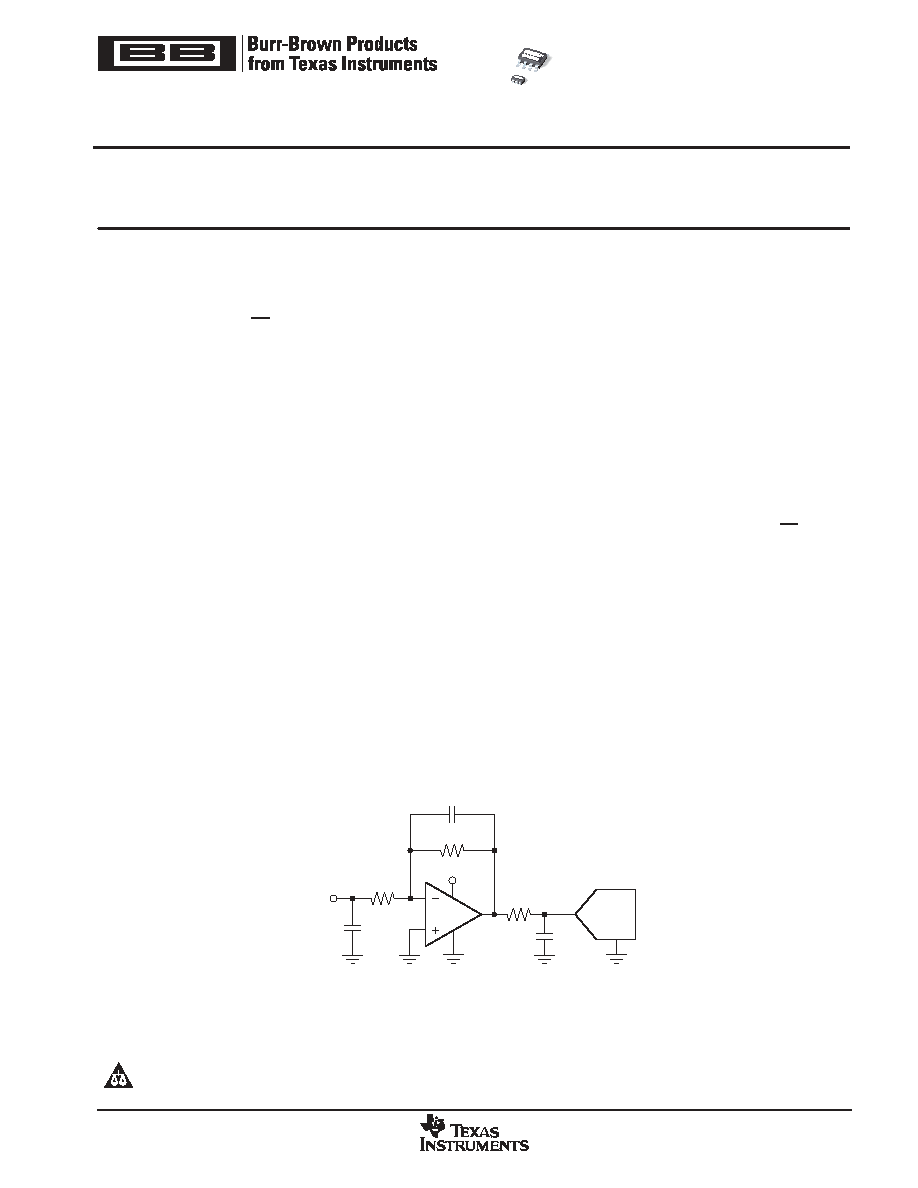
Typical Application
ADS8401
10
V
IN
1.5nF
130pF
(mica)
OPA30x
1820
f
S
= 1.25MSPS
f = 10kHz
5V
130pF
(mica)
1820
All trademarks are the property of their respective owners.
OPA300, OPA2300
OPA301, OPA2301
SBOS271B - MAY 2003 - REVISED JUNE 2005
Low-Noise, High-Speed, 16-Bit Accurate, CMOS
OPERATIONAL AMPLIFIER
PRODUCTION DATA information is current as of publication date. Products
conform to specifications per the terms of Texas Instruments standard warranty.
Production processing does not necessarily include testing of all parameters.
www.ti.com
Copyright
2003-2005, Texas Instruments Incorporated
Please be aware that an important notice concerning availability, standard warranty, and use in critical applications of Texas Instruments
semiconductor products and disclaimers thereto appears at the end of this data sheet.

OPA300, OPA2300
OPA301, OPA2301
SBOS271B - MAY 2003 - REVISED JUNE 2005
www.ti.com
2
PACKAGE/ORDERING INFORMATION
(1)
PRODUCT
PACKAGE-LEAD
PACKAGE DESIGNATOR
PACKAGE MARKING
OPA300
SO-8
D
300A
OPA300
SO-8
D
300A
OPA300
SOT23-6
DBV
A52
OPA300
SOT23-6
DBV
A52
OPA301
SO-8
D
301A
OPA301
SO-8
D
301A
OPA301
SOT23-5
DBV
AUP
OPA301
SOT23-5
DBV
AUP
OPA2300
MSOP-10
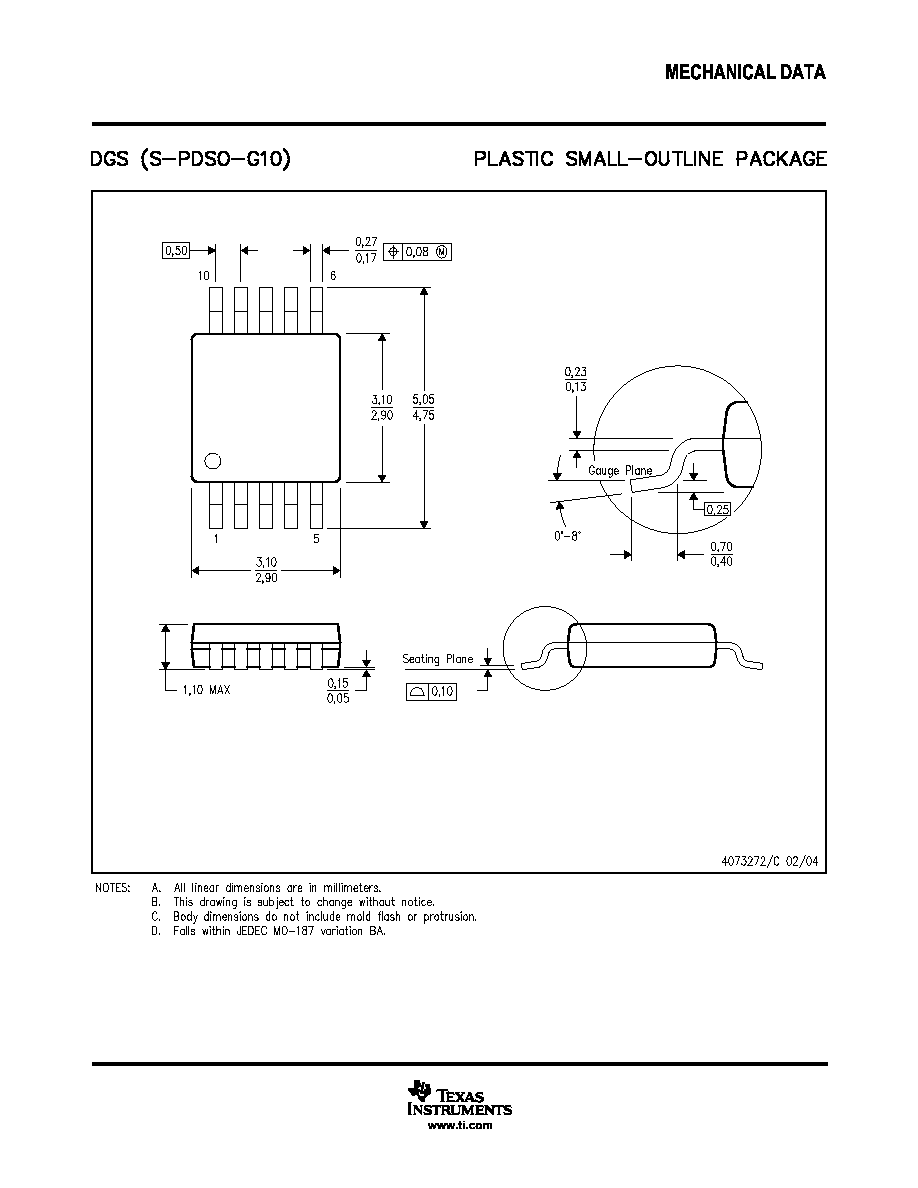
DGS
C01
OPA2301
SO-8
D
OPA2301A
OPA2301
MSOP-8
DGK
C02
(1) For the most current package and ordering information, see the Package Option Addendum at the end of this document, or see the TI website
at www.ti.com.
ABSOLUTE MAXIMUM RATINGS
over operating free-air temperature range unless otherwise noted(1)
Power Supply V+
7V
. . . . . . . . . . . . . . . . . . . . . . . . . . . . . . . . . . . . . .
Signal Input Terminals(2), Voltage
0.5V to (V+) + 0.5V
. . . . . . . . . . .
Current
±
10mA
. . . . . . . . . . . . . . . . . . . . .
Open Short-Circuit Current(3)
Continuous
. . . . . . . . . . . . . . . . . . . .
Operating Temperature Range
-55
∞
C to +125
∞
C
. . . . . . . . . . . . . . .
Storage Temperature Range
-60
∞
C to +150
∞
C
. . . . . . . . . . . . . . . . .
Junction Temperature
+150
∞
C
. . . . . . . . . . . . . . . . . . . . . . . . . . . . . . .
Lead Temperature (soldering, 10s)
+300
∞
C
. . . . . . . . . . . . . . . . . . . . .
ESD Ratings
Human Body Model (HBM)
4kV
. . . . . . . . . . . . . . . . . . . . . . . . . . . . .
Charged-Device Model (CDM)
500V
. . . . . . . . . . . . . . . . . . . . . . . .
(1) Stresses above these ratings may cause permanent damage.
Exposure to absolute maximum conditions for extended periods
may degrade device reliability. These are stress ratings only, and
functional operation of the device at these or any other conditions
beyond those specified is not implied.
(2) Input terminals are diode clamped to the power-supply rails. Input
signals that can swing more than 0.5V beyond the supply rails
should be current limited to 10mA or less.
(3) Short-circuit to ground; one amplifier per package.
ELECTROSTATIC DISCHARGE SENSITIVITY
This integrated circuit can be damaged by ESD. Texas
Instruments recommends that all integrated circuits be
handled with appropriate precautions. Failure to observe
proper handling and installation procedures can cause damage.
ESD damage can range from subtle performance degradation to
complete device failure. Precision integrated circuits may be more
susceptible to damage because very small parametric changes could
cause the device not to meet its published specifications.
PIN ASSIGNMENTS
Top View
MSOP, SO, SOT
NOTE: (1) Not connected. (2) SOT23-6 pin 1 oriented as shown with reference to package marking.
1
2
3
4
8
7
6
5
Enable
V+
V
OUT
NC
(1)
NC
(1)
-
In
+In
V
-
OPA300
SO-8
1
2
3
4
8
7
6
5
NC
(1)
V+
V
OUT
NC
(1)
NC
(1)
-
In
+In
V
-
OPA301
SO-8
1
2
3
5
4
V+
-
In
Out
V
-
+In
OPA301
SOT23-5
1
2
3
6
5
4
V+
Enable
-
In
Out
V
-
+In
OPA300
SOT23-6
(2)
A5
2
1
2
3
4
8
7
6
5
V+
Out B
-
In B
+In B
Out A
-
In A
+In A
V
-
A
B
OPA2301
SO-8, MSOP-8
1
2
3
4
5
10
9
8
7
6
V+
Out B
-
In B
+In B
Enable B
Out A
-
In A
+In A
V
-
Enable A
A
B
OPA2300
MSOP-10

OPA300, OPA2300
OPA301, OPA2301
SBOS271B - MAY 2003 - REVISED JUNE 2005
www.ti.com
3
ELECTRICAL CHARACTERISTICS: V
S
= 2.7V to 5.5V
Boldface limits apply over the temperature range, T
A
= -40
∞
C to +125
∞
C.
All specifications at TA = +25
∞
C, RL = 2k
connected to VS/2, VOUT = VS/2, and VCM = VS/2, unless otherwise noted.
OPA300, OPA301
OPA2300, OPA2301
PARAMETER
TEST CONDITIONS
MIN
TYP
MAX
UNITS
OFFSET VOLTAGE
Input Offset Voltage
VOS
VS = 5V
1
5
mV
Over Temperature
7
mV
Drift
dV
OS
/dT
2.5
µ
V/
∞
C
vs. Power Supply
PSRR
VS = 2.7V to 5.5V, VCM < (V+) ≠0.9V
50
200
µ
V/V
Channel Separation, dc
140
dB
f = 5MHz
100
dB
INPUT VOLTAGE RANGE
Common-Mode Voltage Range
VCM
(V-) - 0.2
(V+) - 0.9
V
Common-Mode Rejection Ratio
CMRR
(V-) - 0.2V < VCM < (V+) ≠ 0.9V
66
80
dB
INPUT BIAS CURRENT
Input Bias Current
IB
±
0.1
±
5
pA
Input Offset Current
IOS
±
0.5
±
5
pA
INPUT IMPEDANCE
Differential
1013 || 3
|| pF
Common-Mode
1013 || 6
|| pF
NOISE
Input Voltage Noise, f = 0.1Hz to 1MHz
40
µ
V
PP
Input Voltage Noise Density, f > 1MHz
en
3
nV/
Hz
Input Current Noise Density, f < 1kHz
in
1.5
fA/
Hz
Differential Gain Error
NTSC, RL = 150
0.01
%
Differential Phase Error
NTSC, RL = 150
0.1
∞
OPEN-LOOP GAIN
Open-Loop Voltage Gain
AOL
VS = 5V, RL = 2k
, 0.1V < VO < 4.9V
95
106
dB
Over Temperature
VS = 5V, RL = 2k
, 0.1V < VO < 4.9V
90
dB
VS = 5V, RL = 100
, 0.5V < VO < 4.5V
95
106
dB
Over Temperature
VS = 5V, RL = 100
, 0.5V < VO < 4.5V
90
dB
OUTPUT
Voltage Output Swing from Rail
RL = 2k
, AOL > 95dB
75
100
mV
RL = 100
, AOL > 95dB
300
500
mV
Short-Circuit Current
ISC
70
mA
Capacitive Load Drive
CLOAD
See Typical Characteristics
FREQUENCY RESPONSE
Gain-Bandwidth Product
GBW
150
MHz
Slew Rate
SR
G = +1
80
V/
µ
s
Settling Time, 0.01%
tS
VS = 5V, 2V Step, G = +1
90
ns
0.1%
30
ns
Overload Recovery Time
Gain = -1
30
ns
Total Harmonic Distortion + Noise
THD+N
VS = 5V, VO = 3V
PP
, G = +1, f = 1kHz
0.003
%
POWER SUPPLY
Specified Voltage Range
VS
2.7
5.5
V
Operating Voltage Range
2.7 to 5.5
V
Quiescent Current (per amplifier)
IQ
IO = 0
9.5
12
mA
Over Temperature
13
mA
SHUTDOWN
tOFF
40
ns
tON
5
µ
s
VL (shutdown)
(V-) - 0.2
(V-) + 0.8
V
VH (amplifier is active)
(V-) + 2.5
(V+) + 0.2
V
IQSD (per amplifier)
3
10
µ
A
TEMPERATURE RANGE
Specified Range
-40
+125
∞
C
Operating Range
-55
+125
∞
C
Storage Range
-60
+150
∞
C
Thermal Resistance
JA
∞
C/W
SO-8, MSOP-8, MSOP-10
150
∞
C/W
SOT23-5, SOT23-6
200
∞
C/W
OPA300, OPA2300
OPA301, OPA2301
SBOS271B - MAY 2003 - REVISED JUNE 2005
www.ti.com
4
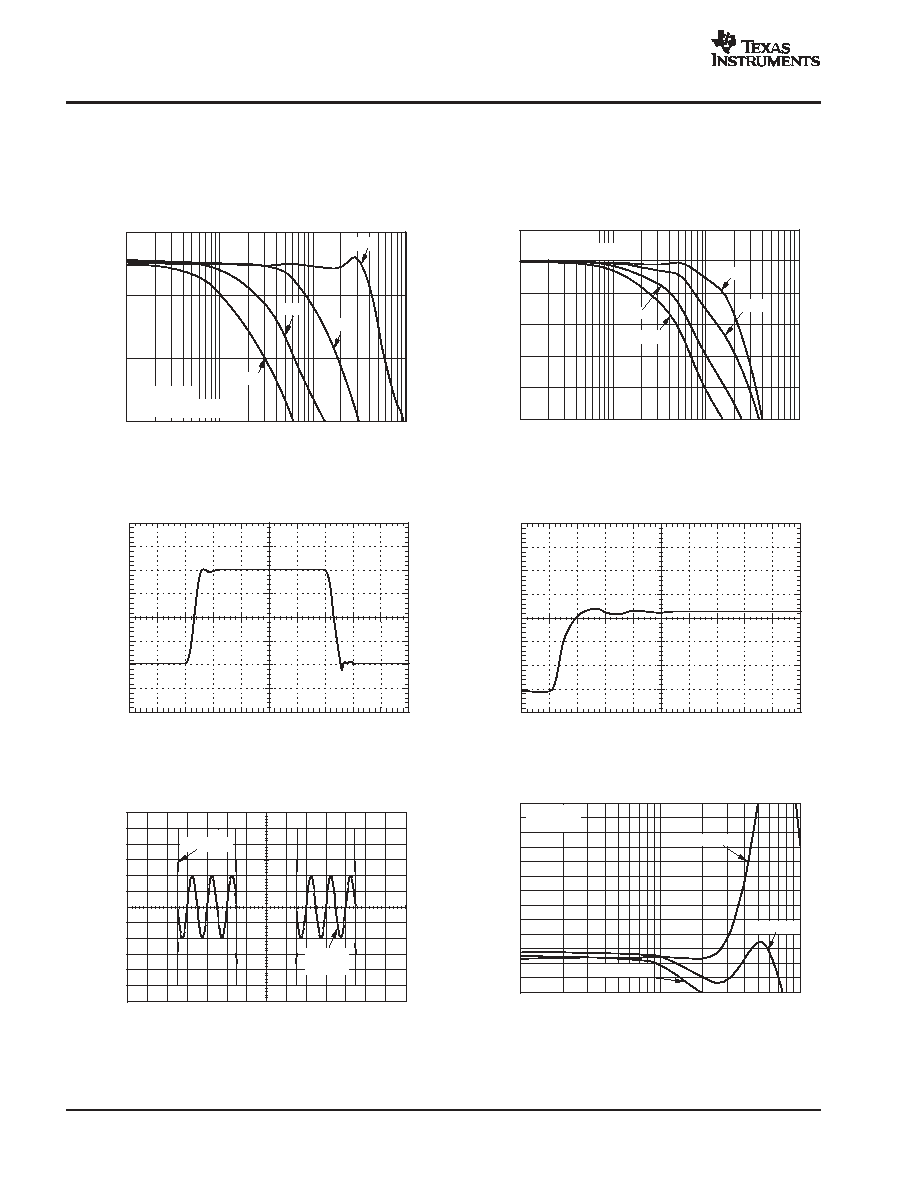
TYPICAL CHARACTERISTICS
All specifications at TA = 25
∞
C, VS = 5V, and RL = 150
connected to VS/2 unless otherwise noted.
NONINVERTING GAIN
SMALL-SIGNAL FREQUENCY RESPONSE
Frequency (Hz)
1M
10M
100M
1G
3
-
3
-
9
-
15
N
o
r
m
a
liz
e
d
G
a
i
n
(
d
B
)
G = 2
G = 1
G = 5
G = 10
V
O
= 0.1V
PP
R
F
= 310
for G > 1
LARGE-SIGNAL STEP RESPONSE
Time (50ns/div)
O
u
tput
V
o
l
t
age
(
5
0
0
mV
/di
v
)
LARGE-SIGNAL ENABLE/DISABLE RESPONSE
Time (100
µ
s/div)
O
u
t
p
u
t
V
o
l
t
ag
e
(
500mV
/
d
i
v
)
Enable Pin
Amplifier
Output
INVERTING GAIN
SMALL-SIGNAL FREQUENCY RESPONSE
Frequency (Hz)
1M
10M
100M
1G
3
0
-
3
-
6
-
9
-
12
-
15
N
o
rm
a
l
i
z
e
d
Ga
i
n
(d
B
)
G =
-
2
G =
-
1
G =
-
5
G =
-
10
V
O
= 0.1V
PP
R
F
= 310
for G > 1
O
u
t
p
ut
V
o
l
t
ag
e
(
1
0
m
V
/
d
i
v
)
Time (5ns/div)
SMALL-SIGNAL STEP RESPONSE
V
OUT
0.1dB GAIN FLATNESS FOR VARIOUS R
F
Frequency (MHz)
1
10
100
1.0
0.9
0.8
0.7
0.6
0.5
0.4
0.3
0.2
0.1
0
-
0.1
-
0.2
-
0.3
N
o
r
m
a
liz
e
d
G
a
i
n
(
d
B
)
R
F
= 825
Gain = 2
V
O
= 0.1V
PP
R
F
= 450
R
F
= 205
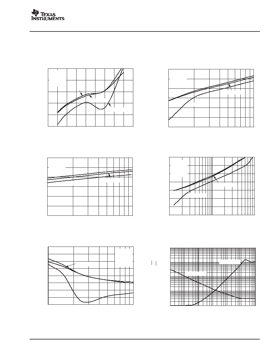
OPA300, OPA2300
OPA301, OPA2301
SBOS271B - MAY 2003 - REVISED JUNE 2005
www.ti.com
5
TYPICAL CHARACTERISTICS (continued)
All specifications at TA = 25
∞
C, VS = 5V, and RL = 150
connected to VS/2 unless otherwise noted.
HARMONIC DISTORTION vs OUTPUT VOLTAGE
Output Voltage (V
PP
)
0
0.5
1.0
1.5
2.0
2.5
3.0
3.5
4.0
4.5
-
50
-
60
-
70
-
80
-
90
-
100
Ha
r
m
o
n
i
c
Di
s
t
o
r
t
i
o
n
(
d
B
c
)
THD
2nd-Harmonic
3rd-Harmonic
R
L
= 200
f = 1MHz
R
F
= 310
G = 2
HARMONIC DISTORTION vs INVERTING GAIN
Gain (V/V)
1
10
-
50
-
60
-
70
-
80
-
90
-
100
-
110
H
a
rm
o
n
i
c
D
i
s
t
o
rt
i
o
n
(
d
B
c
)
THD
2nd-Harmonic
3rd-Harmonic
V
O
= 2V
PP
R
L
= 200
f = 1MHz
R
F
= 310
HARMONIC DISTORTION vs LOAD RESISTANCE
Load Resistance (
)
100
1k
-
60
-
65
-
70
-
75
-
80
-
85
-
90
-
95
-
100
Ha
r
m
o
n
i
c
Di
s
t
o
r
ti
o
n
(
d
B
c
)
THD
2nd-Harmonic
3rd-Harmonic
V
O
= 2V
PP
f = 1MHz
Gain = 2
R
F
= 310
HARMONIC DISTORTION vs NONINVERTING GAIN
Gain (V/V)
1
10
-
50
-
60
-
70
-
80
-
90
-
100
-
110
H
a
rm
o
n
i
c
D
i
s
t
o
rt
i
o
n
(
d
B
c)
THD
2nd-Harmonic
3rd-Harmonic
V
O
= 2V
PP
R
L
= 200
f = 1MHz
R
F
= 310
HARMONIC DISTORTION vs FREQUENCY
Frequency (Hz)
100k
1M
10M
-
50
-
60
-
70
-
80
-
90
-
100
-
110
-
120
Ha
r
m
o
n
i
c
Di
s
t
o
r
ti
o
n
(
d
B
c
)
THD
2nd-Harmonic
3rd-Harmonic
V
O
= 2V
PP
R
L
= 200
Gain = 2
R
F
= 310
INPUT VOLTAGE AND CURRENT NOISE
SPECTRAL DENSITY vs FREQUENCY
Frequency (Hz)
10
100
1k
10k
100k
1M
10M
10k
1k
100
10
1
Vo
l
t
a
g
e
N
o
i
s
e
(
n
V
/
Hz
)
Cu
r
r
e
n
t
No
i
s
e
(
fA
/
Hz
)
Voltage Noise
Current Noise

OPA300, OPA2300
OPA301, OPA2301
SBOS271B - MAY 2003 - REVISED JUNE 2005
www.ti.com
6
TYPICAL CHARACTERISTICS (continued)
All specifications at TA = 25
∞
C, VS = 5V, and RL = 150
connected to VS/2 unless otherwise noted.
FREQUENCY RESPONSE FOR VARIOUS R
L
Frequency (Hz)
10M
100M
500
9
3
-
3
-
9
-
15
-
21
Ga
i
n
(d
B
)
R
LOAD
= 1k
R
LOAD
= 150
R
LOAD
= 50
Gain = 1
V
O
= 0.1V
PP
COMMON-MODE REJECTION RATIO AND
POWER-SUPPLY REJECTION RATIO vs FREQUENCY
Frequency (Hz)
10k
100k
1M
10M
100M
1G
100
90
80
70
60
50
40
30
20
10
0
PS
R
R
(
d
B
)
CM
RR
(
d
B
)
CMRR
PSRR V
-
PSRR V+
COMPOSITE VIDEO
DIFFERENTIAL GAIN AND PHASE
Number of 150
Loads
1
2
3
4
1.0
0.8
0.6
0.4
0.2
0
dP
(
_
)
dG
(
%
)
dP
dG
FREQUENCY RESPONSE vs CAPACITIVE LOAD
Frequency (Hz)
10M
100M
500
3
-
3
-
9
-
15
-
21
-
27
N
o
r
m
a
liz
e
d
G
a
i
n
(
d
B
)
C
LOAD
= 100pF
R
S
= 20
C
LOAD
= 47pF
R
S
= 30
C
LOAD
= 1pF, R
S
= 75
C
LOAD
= 5pF
R
S
= 55
C
LOAD
= 10pF
R
S
= 40
R
S
C
L
OPEN-LOOP GAIN AND PHASE vs FREQUENCY
Frequency (Hz)
10k
1k
100
100k
1M
10M
100M
1G
110
100
90
80
70
60
50
40
30
20
10
0
-
10
0
-
30
-
60
-
90
-
120
-
150
-
180
Ga
i
n
(d
B
)
Ph
a
s
e
(
_
)
Phase
Gain
OUTPUT VOLTAGE SWING vs OUTPUT CURRENT
Output Current (mA)
0
10
20
30
40
50
60
70
80
5.0
4.0
3.0
2.0
1.0
0
O
u
t
p
u
t
Vo
l
t
a
g
e
(
V)
V
S
= 5V
125
_
C 85
_
C
25
_
C
25
_
C
-
40
_
C
-
55
_
C
OPA300, OPA2300
OPA301, OPA2301
SBOS271B - MAY 2003 - REVISED JUNE 2005
www.ti.com
7
TYPICAL CHARACTERISTICS (continued)
All specifications at TA = 25
∞
C, VS = 5V, and RL = 150
connected to VS/2 unless otherwise noted.
OUTPUT VOLTAGE SWING vs OUTPUT CURRENT
Output Current (mA)
0
10
20
30
40
50
60
70
80
2.7
2.4
2.1
1.8
1.5
1.2
0.9
0.6
0.3
0
O
u
t
put
V
o
l
t
a
g
e
(
V
)
V
S
= 2.7V
125
_
C 85
_
C 25
_
C
-
40
_
C
-
55
_
C
QUIESCENT CURRENT vs TEMPERATURE
Temperature (
_
C)
-
40
-
20
0
20
40
60
80
100
140
120
12
11
10
9
8
7
6
Q
u
i
e
sce
n
t
C
u
rre
n
t
(
m
A)
POWER-SUPPLY REJECTION RATIO AND
COMMON-MODE REJECTION RATIO vs TEMPERATURE
Temperature (
_
C)
-
40
-
20
0
20
40
60
80
100
120
140
100
95
90
85
80
75
70
65
60
PS
R
R
(
d
B)
CM
RR
(
d
B
)
PSRR
CMRR
INPUT BIAS CURRENT vs TEMPERATURE
Temperature (
_
C)
-
40
-
20
0
20
40
60
80
100
140
120
1
0.1
0.01
Inpu
t
B
i
a
s
C
u
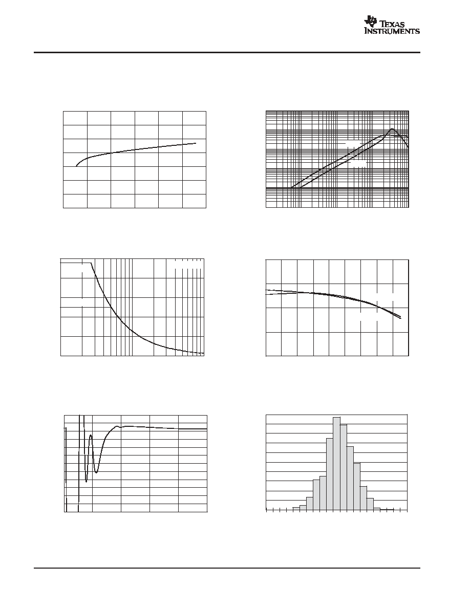
r
r
ent
(
p
A
)
INPUT BIAS CURRENT vs COMMON-MODE VOLTAGE
Common-Mode Voltage (V)
-
3
-
2
-
1
0
1
2
2
1
0
-
1
-
2
Inpu
t
B
i
a
s
C
ur
r
ent
(
p
A
)
V
S
=
±
2.5V
SHORT-CIRCUIT CURRENT vs TEMPERATURE
Temperature (
_
C)
80
60
40
20
0
-
20
-
40
-
60
-
80
Sh
o
r
t
-
C
i
rc
u
i
t
C
u
r
r
e
n
t
(m
A
)
-
40
-
20
0
20
40
60
80
100
120
140
V
S
= 5.5V
V
S
= 5V
V
S
= 5.5V
V
S
= 2.7V
V
S
= 3.5V
OPA300, OPA2300
OPA301, OPA2301
SBOS271B - MAY 2003 - REVISED JUNE 2005
www.ti.com
8
TYPICAL CHARACTERISTICS (continued)
All specifications at TA = 25
∞
C, VS = 5V, and RL = 150
connected to VS/2 unless otherwise noted.
QUIESCENT CURRENT vs SUPPLY VOLTAGE
Supply Voltage (V)
2.5
3
3.5
4
5
4.5
5.5
12
11
10
9
8
7
6
5
Q
u
i
e
s
c
ent
C
u
r
r
e
nt
(
m
A
)
MAXIMUM OUTPUT VOLTAGE vs FREQUENCY
Frequency (MHz)
1
10
100
5
4
3
2
1
0
Ou
t
p
u
t
V
o
l
t
a
g
e
(
V
PP
)
V
S
= 5V
V
S
= 2.7V
R
LOAD
= 2k
OUTPUT SETTLING TIME TO 0.1%
Time (ns)
0
20
40
60
80
100
0.2
0.1
0
-
0.1
-
0.2
-
0.3
-
0.4
-
0.5
-
0.6
-
0.7
-
0.8
-
0.9
-
1.0
Ou
t
p
u
t
E
r
r
o
r
(
%
)
OUTPUT IMPEDANCE vs FREQUENCY
Frequency (Hz)
10k
100k
1M
10M
100M
1000
100
10
1
0.1
0.01
O
u
t
p
u
t
Im
p
e
dan
c
e
,
Z
O
(
)
G = 2
G = 1
OPEN-LOOP GAIN vs TEMPERATURE
Temperature (
_
C)
-
40
-
20
0
20
40
60
80
100
120
140
120
110
100
90
80
O
p
e
n
-
L
o
o
pG
a
i
n(
d
B
)
R
LOAD
= 2k
R
LOAD
= 100
OFFSET VOLTAGE
PRODUCTION DISTRIBUTION
Offset Voltage (mV)
-
5
-
4
-
3
-
2
-
1
0
1
3
4
2
5
20
18
16
14
12
10
8
6
4
2
0
P
e
r
c
ent
of
A
m
pl
i
f
i
e
r
s
OPA300, OPA2300
OPA301, OPA2301
SBOS271B - MAY 2003 - REVISED JUNE 2005
www.ti.com
9
TYPICAL CHARACTERISTICS (continued)
All specifications at TA = 25
∞
C, VS = 5V, and RL = 150
connected to VS/2 unless otherwise noted.
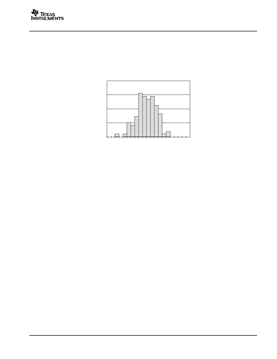
OFFSET VOLTAGE DRIFT
PRODUCTION DISTRIBUTION
Offset Voltage Drift (
µ
V/
_
C)
-
10
-
8
-
6
-
4
-
2
0
2
6
8
4
10
20
15
10
5
0
Pe
r
c
e
n
t
o
f
Am
p
lif
i
e
r
s
OPA300, OPA2300
OPA301, OPA2301
SBOS271B - MAY 2003 - REVISED JUNE 2005
www.ti.com
10
APPLICATIONS INFORMATION
The OPA300 and OPA301 series of single-supply
CMOS op amps are designed to interface with
high-speed 16-bit analog-to-digital converters (ADCs).
Featuring wide 150MHz bandwidth, fast 150ns settling
time to 16 bits, and high open loop gain, this series
offers excellent performance in a small SO-8 and tiny
SOT23 packages.
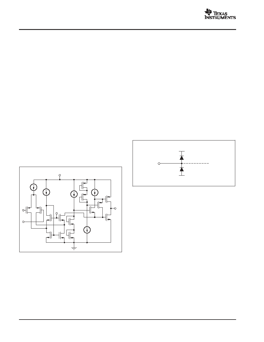
THEORY OF OPERATION
The OPA300 and OPA301 series op amps use a classic
two-stage topology, shown in Figure 1. The differential
input pair is biased to maximize slew rate without
compromising stability or bandwidth. The folded
cascode adds the signal from the input pair and
presents a differential signal to the class AB output
stage. The class AB output stage allows rail- to-rail
output swing, with high-impedance loads
(> 2k
), typically 100mV from the supply rails. With 10
loads, a useful output swing can be achieved and still
maintain high open-loop gain. See the typical
characteristic Output Voltage Swing vs Output Current.
+V
S
V
BIAS
+
V
IN
-
V
OUT
Figure 1. OPA30x Classic Two-Stage Topology
OPERATING VOLTAGE
OPA300/OPA301 series op amp parameters are fully
specified from +2.7V to +5.5V. Supply voltages higher
than 5.5V (absolute maximum) can cause permanent
damage to the amplifier. Many specifications apply from
≠40
∞
C to +125
∞
C. Parameters that vary significantly
with operating voltages or temperature are shown in the
Typical Characteristics.
PCB LAYOUT
As with most high-speed operational amplifiers, board
layout requires special attention to maximize AC and
DC performance. Extensive use of ground planes, short
lead lengths, and high-quality bypass capacitors will
minimize leakage that can compromise signal quality.
Guard rings applied with potential as near to the input
pins as possible help minimize board leakage.
INPUT AND ESD PROTECTION
All OPA300/OPA301 series op amps' pins are static-
protected with internal ESD protection diodes tied to the
supplies, as shown in Figure 2. These diodes will
provide overdrive protection if the current is externally
limited to 10mA, as stated in the Absolute Maximum
Ratings. Any input current beyond the Absolute
Maximum Ratings, or long-term operation at maximum
ratings, will shorten the lifespan of the amplifier.
External
Pin
+V
-
V
Internal
Circuitry
Figure 2. ESD Protection Diodes
ENABLE FUNCTION
The shutdown function of the OPA300 and OPA2300 is
referenced to the negative supply voltage of the
operational amplifier. A logic level HIGH enables the op
amp. A valid logic HIGH is defined as 2.5V above the
negative supply applied to the enable pin. A valid logic
LOW is defined as < 0.8V above the negative supply
pin. If dual or split power supplies are used, care should
be taken to ensure logic input signals are properly
referred to the negative supply voltage. If this pin is not
connected to a valid high or low voltage, the internal
circuitry will pull the node high and enable the part to
function.
The logic input is a high-impedance CMOS input. For
battery-operated applications, this feature may be used
to greatly reduce the average current and extend
battery life. The enable time is 10
µ
s; disable time is 1
µ
s.
When disabled, the output assumes a high-impedance
state. This allows the OPA300 to be operated as a gated
amplifier, or to have its output multiplexed onto a
common analog output bus.

OPA300, OPA2300
OPA301, OPA2301
SBOS271B - MAY 2003 - REVISED JUNE 2005
www.ti.com
11
DRIVING CAPACITIVE LOADS
When using high-speed operational amplifiers, it is
extremely important to consider the effects of
capacitive loading on amplifier stability. Capacitive
loading will interact with the output impedance of the
operational amplifier, and depending on the capacitor
value, may significantly decrease the gain bandwidth,
as well as introduce peaking. To reduce the effects of
capacitive loading and allow for additional capacitive
load drive, place a series resistor between the output
and the load. This will reduce available bandwidth, but
permit stable operation with capacitive loading.
Figure
3 illustrates the recommended relationship
between the resistor and capacitor values.
Capacitive Load (pF)
1
10
100
100
75
50
25
0
S
e
r
i
e
s
R
e
s
i
s
t
anc
e
(
)
Figure 3. Recommended R
S
and C
L
Combinations
Amplifiers configured in unity gain are most susceptible
to stability issues. The typical characteristic, Frequency
Response vs Capacitive Load, describes the relation-
ship between capacitive load and stability for the
OPA300/OPA301 series. In unity gain, the
OPA300/OPA301 series is capable of driving a few
picofarads of capacitive load without compromising
stability. Board level parasitic capacitance can often fall
into the range of a picofarad or more, and should be
minimized through good circuit-board layout practices
to avoid compromising the stability of the
OPA300/OPA301. For more information on detecting
parasitics during testing, see the Application Note
Measuring Board Parasitics in High-Speed Analog
Design (SBOA094), available at the TI web site
www.ti.com.
DRIVING A 16-BIT ADC
The OPA300/OPA301 series feature excellent
THD+noise, even at frequencies greater than 1MHz,
with a 16-bit settling time of 150ns. Figure 4 shows a
total single supply solution for high-speed data
acquisition. The OPA300/OPA301 directly drives the
ADS8401, a 1.25 mega sample per second (MSPS)
16-bit data converter. The OPA300/OPA301 is
configured in an inverting gain of 1, with a 5V single
supply. Results of the OPA300/OPA301 performance
are summarized in Table 1.
ADS8401
10
V
IN
1.5nF
130pF
(mica)
OPA30x
1820
f
S
= 1.25MSPS
f = 10kHz
5V
130pF
(mica)
1820
Figure 4. The OPA30x Drives the 16-Bit ADS8401
PARAMETER
RESULTS (f = 10kHz)
THD
-99.3dB
SFDR
101.2dB
THD+N
84.2dB
SNR
84.3dB
Table
1. OPA30x Performance Results Driving a
1.25MSPS ADS8401

PACKAGING INFORMATION
Orderable Device
Status
(1)
Package
Type
Package
Drawing
Pins Package
Qty
Eco Plan
(2)
Lead/Ball Finish
MSL Peak Temp
(3)
OPA2300AIDGSR
ACTIVE
MSOP
DGS
10
2500 Green (RoHS &
no Sb/Br)
CU NIPDAU
Level-2-260C-1 YEAR
OPA2300AIDGSRG4
ACTIVE
MSOP
DGS
10
2500 Green (RoHS &
no Sb/Br)
CU NIPDAU
Level-2-260C-1 YEAR
OPA2300AIDGST
ACTIVE
MSOP
DGS
10
250
Green (RoHS &
no Sb/Br)
CU NIPDAU
Level-2-260C-1 YEAR
OPA2300AIDGSTG4
ACTIVE
MSOP
DGS
10
250
Green (RoHS &
no Sb/Br)
CU NIPDAU
Level-2-260C-1 YEAR
OPA2301AID
ACTIVE
SOIC
D
8
75
Green (RoHS &
no Sb/Br)
CU NIPDAU
Level-2-260C-1 YEAR
OPA2301AIDG4
ACTIVE
SOIC
D
8
75
Green (RoHS &
no Sb/Br)
CU NIPDAU
Level-2-260C-1 YEAR
OPA2301AIDGKR
ACTIVE
MSOP
DGK
8
2500 Green (RoHS &
no Sb/Br)
CU NIPDAU
Level-2-260C-1 YEAR
OPA2301AIDGKRG4
ACTIVE
MSOP
DGK
8
2500 Green (RoHS &
no Sb/Br)
CU NIPDAU
Level-2-260C-1 YEAR
OPA2301AIDGKT
ACTIVE
MSOP
DGK
8
250
Green (RoHS &
no Sb/Br)
CU NIPDAU
Level-2-260C-1 YEAR
OPA2301AIDGKTG4
ACTIVE
MSOP
DGK
8
250
Green (RoHS &
no Sb/Br)
CU NIPDAU
Level-2-260C-1 YEAR
OPA2301AIDR
ACTIVE
SOIC
D
8
2500 Green (RoHS &
no Sb/Br)
CU NIPDAU
Level-2-260C-1 YEAR
OPA2301AIDRG4
ACTIVE
SOIC
D
8
2500 Green (RoHS &
no Sb/Br)
CU NIPDAU
Level-2-260C-1 YEAR
OPA300AID
ACTIVE
SOIC
D
8
100
TBD
CU NIPDAU
Level-3-235C-168 HR
OPA300AIDBVR
ACTIVE
SOT-23
DBV
6
3000
TBD
CU SNPB
Level-2-240C-1 YEAR
OPA300AIDBVT
ACTIVE
SOT-23
DBV
6
250
TBD
CU SNPB
Level-2-240C-1 YEAR
OPA300AIDR
ACTIVE
SOIC
D
8
2500
TBD
CU NIPDAU
Level-3-235C-168 HR
OPA301AID
ACTIVE
SOIC
D
8
100
TBD
CU NIPDAU
Level-3-240C-168 HR
OPA301AIDBVR
ACTIVE
SOT-23
DBV
5
3000
TBD
CU NIPDAU
Level-1-235C-UNLIM
OPA301AIDBVT
ACTIVE
SOT-23
DBV
5
250
TBD
CU NIPDAU
Level-1-235C-UNLIM
OPA301AIDR
ACTIVE
SOIC
D
8
2500
TBD
CU NIPDAU
Level-3-240C-168 HR
(1)
The marketing status values are defined as follows:
ACTIVE: Product device recommended for new designs.
LIFEBUY: TI has announced that the device will be discontinued, and a lifetime-buy period is in effect.
NRND: Not recommended for new designs. Device is in production to support existing customers, but TI does not recommend using this part in
a new design.
PREVIEW: Device has been announced but is not in production. Samples may or may not be available.
OBSOLETE: TI has discontinued the production of the device.
(2)
Eco
Plan
-
The
planned
eco-friendly
classification:
Pb-Free
(RoHS)
or
Green
(RoHS
&
no
Sb/Br)
-
please
check
http://www.ti.com/productcontent
for the latest availability information and additional product content details.
TBD: The Pb-Free/Green conversion plan has not been defined.
Pb-Free (RoHS): TI's terms "Lead-Free" or "Pb-Free" mean semiconductor products that are compatible with the current RoHS requirements
for all 6 substances, including the requirement that lead not exceed 0.1% by weight in homogeneous materials. Where designed to be soldered
at high temperatures, TI Pb-Free products are suitable for use in specified lead-free processes.
Green (RoHS & no Sb/Br): TI defines "Green" to mean Pb-Free (RoHS compatible), and free of Bromine (Br) and Antimony (Sb) based flame
retardants (Br or Sb do not exceed 0.1% by weight in homogeneous material)
(3)
MSL, Peak Temp. -- The Moisture Sensitivity Level rating according to the JEDEC industry standard classifications, and peak solder
PACKAGE OPTION ADDENDUM
www.ti.com
22-Nov-2005
Addendum-Page 1

temperature.
Important Information and Disclaimer:The information provided on this page represents TI's knowledge and belief as of the date that it is
provided. TI bases its knowledge and belief on information provided by third parties, and makes no representation or warranty as to the
accuracy of such information. Efforts are underway to better integrate information from third parties. TI has taken and continues to take
reasonable steps to provide representative and accurate information but may not have conducted destructive testing or chemical analysis on
incoming materials and chemicals. TI and TI suppliers consider certain information to be proprietary, and thus CAS numbers and other limited
information may not be available for release.
In no event shall TI's liability arising out of such information exceed the total purchase price of the TI part(s) at issue in this document sold by TI
to Customer on an annual basis.
PACKAGE OPTION ADDENDUM
www.ti.com
22-Nov-2005
Addendum-Page 2


IMPORTANT NOTICE
Texas Instruments Incorporated and its subsidiaries (TI) reserve the right to make corrections, modifications,
enhancements, improvements, and other changes to its products and services at any time and to discontinue
any product or service without notice. Customers should obtain the latest relevant information before placing
orders and should verify that such information is current and complete. All products are sold subject to TI's terms
and conditions of sale supplied at the time of order acknowledgment.
TI warrants performance of its hardware products to the specifications applicable at the time of sale in
accordance with TI's standard warranty. Testing and other quality control techniques are used to the extent TI
deems necessary to support this warranty. Except where mandated by government requirements, testing of all
parameters of each product is not necessarily performed.
TI assumes no liability for applications assistance or customer product design. Customers are responsible for
their products and applications using TI components. To minimize the risks associated with customer products
and applications, customers should provide adequate design and operating safeguards.
TI does not warrant or represent that any license, either express or implied, is granted under any TI patent right,
copyright, mask work right, or other TI intellectual property right relating to any combination, machine, or process
in which TI products or services are used. Information published by TI regarding third-party products or services
does not constitute a license from TI to use such products or services or a warranty or endorsement thereof.
Use of such information may require a license from a third party under the patents or other intellectual property
of the third party, or a license from TI under the patents or other intellectual property of TI.
Reproduction of information in TI data books or data sheets is permissible only if reproduction is without
alteration and is accompanied by all associated warranties, conditions, limitations, and notices. Reproduction
of this information with alteration is an unfair and deceptive business practice. TI is not responsible or liable for
such altered documentation.
Resale of TI products or services with statements different from or beyond the parameters stated by TI for that
product or service voids all express and any implied warranties for the associated TI product or service and
is an unfair and deceptive business practice. TI is not responsible or liable for any such statements.
Following are URLs where you can obtain information on other Texas Instruments products and application
solutions:
Products
Applications
Amplifiers
amplifier.ti.com
Audio
www.ti.com/audio
Data Converters
dataconverter.ti.com
Automotive
www.ti.com/automotive
DSP
dsp.ti.com
Broadband
www.ti.com/broadband
Interface
interface.ti.com
Digital Control
www.ti.com/digitalcontrol
Logic
logic.ti.com
Military
www.ti.com/military
Power Mgmt
power.ti.com
Optical Networking
www.ti.com/opticalnetwork
Microcontrollers
microcontroller.ti.com
Security
www.ti.com/security
Telephony
www.ti.com/telephony
Video & Imaging
www.ti.com/video
Wireless
www.ti.com/wireless
Mailing Address:
Texas Instruments
Post Office Box 655303 Dallas, Texas 75265
Copyright
2005, Texas Instruments Incorporated