Document Outline
- FEATURES
- APPLICATIONS
- DESCRIPTION
- ABSOLUTE MAXIMUM RATINGS(
- PACKAGE/ORDERING INFORMATION
- ELECTRICAL CHARACTERISTICS: OPA452; VS = ±10V to ±40V
- ELECTRICAL CHARACTERISTICS: OPA453; VS = ±10V to ±40V
- TYPICAL CHARACTERISTICS
- APPLICATIONS INFORMATION
- CURRENT LIMIT
- THERMAL PROTECTION
- POWER SUPPLIES
- POWER DISSIPATION
- SAFE OPERATING AREA
- HEAT SINKING
- CAPACITIVE LOADS
- INCREASING OUTPUT CURRENT
- INPUT PROTECTION
- USING THE OPA453 IN LOW GAINS

OPA4
52
OPA
452
OPA4
52
7-Lead
Straight-Formed
TO-220 (TA)
NOTE: Tabs are electrically connected to V≠ supply.
NC
V≠
V
O
V+
V
IN≠
V
IN+
1 2 3 4 5 6
Flag
7
7-Lead
DDPAK (FA)
Surface-Mount
NC
V≠
V
O
V+
V
IN≠
V
IN+
1 2 3 4 5 6
Flag
7
7-Lead
Stagger-Formed
TO-220 (TA-1)
NC
V≠
V
O
V+
V
IN≠
V
IN+
1 2 3 4 5 6
Flag
7
80V, 50mA
OPERATIONAL AMPLIFIERS
FEATURES
q
WIDE POWER-SUPPLY RANGE:
±
10V to
±
40V
q
HIGH OUTPUT LOAD DRIVE:
50mA Continuous
q
WIDE OUTPUT VOLTAGE SWING: 1V to Rail
q
FULLY PROTECTED:
Thermal Shutdown
Output Current-Limited
q
WIDE OPERATING TEMPERATURE RANGE:
≠40
∞
C TO +125
∞
C
q
PACKAGE OPTIONS:
TO220-7
DDPACK-7 Surface-Mount
APPLICATIONS
q
PIEZOELECTRIC CELLS
q
TEST EQUIPMENT
q
AUDIO AMPLIFIERS
q
TRANSDUCER DRIVERS
q
SERVO DRIVERS
DESCRIPTION
The OPA452 and OPA453 are low-cost operational amplifi-
ers with high-voltage (80V) and high-current capabilities
(50mA). The OPA452 is unity-gain stable and has a gain
bandwidth product of 1.8MHz, whereas the OPA453 is opti-
mized for gains greater than 5 and has a 7.5MHz bandwidth.
The OPA452 and OPA453 are internally protected against
over-temperature conditions and current overloads. Power
supplies in the range of
±
10V to
±
40V can be used. Unlike
most other power op amps, the OPA452 and OPA453 have
ensured specifications over the entire power-supply range.
These laser-trimmed, monolithic integrated circuits provide
excellent low-level accuracy along with wide output swing.
Special design considerations assure that the product is
easy to use and free from phase inversion problems often
found in other amplifiers.
The OPA452 and OPA453 are available in TO220-7 and
DDPAK-7 options. They are specified for a junction tempera-
ture range of ≠40
∞
C to +125
∞
C.
OPA452
OPA453
SBOS127C ≠ JULY 2000 ≠ REVISED NOVEMBER 2003
www.ti.com
PRODUCTION DATA information is current as of publication date.
Products conform to specifications per the terms of Texas Instruments
standard warranty. Production processing does not necessarily include
testing of all parameters.
Copyright © 2000-2003, Texas Instruments Incorporated
Please be aware that an important notice concerning availability, standard warranty, and use in critical applications of
Texas Instruments semiconductor products and disclaimers thereto appears at the end of this data sheet.

OPA452, 453
2
SBOS127C
www.ti.com
Supply Voltage, V+ to V≠ ................................................................... 80V
Signal Input Terminals, Voltage
(2)
.................. (V≠) ≠ 0.5V to (V+) + 0.5V
Current
(2)
...................................................... 5mA
Output Short-Circuit ................................................................. Continuous
Operating Temperature .................................................. ≠55
∞
C to +125
∞
C
Storage Temperature ..................................................... ≠65
∞
C to +150
∞
C
Junction Temperature .................................................................... +150
∞
C
Lead Temperature (soldering 10s, TO-220) ................................... 300
∞
C
(soldering 3s, DDPAK) ..................................... 240
∞
C
NOTES: (1) Stresses above these ratings may cause permanent damage.
Exposure to absolute maximum conditions for extended periods may degrade
device reliability. (2) Input terminals are diode-clamped to the power-supply
rails. Input signals that can swing more than 0.5V beyond the supply rails
should be current limited to 5mA or less.
PACKAGE/ORDERING INFORMATION
For the most current package and ordering information, see the
Package Option Addendum located at the end of this data
sheet.
ELECTROSTATIC
DISCHARGE SENSITIVITY
This integrated circuit can be damaged by ESD. Texas Instru-
ments recommends that all integrated circuits be handled with
appropriate precautions. Failure to observe proper handling
and installation procedures can cause damage.
ESD damage can range from subtle performance degrada-
tion to complete device failure. Precision integrated circuits
may be more susceptible to damage because very small
parametric changes could cause the device not to meet its
published specifications.
ABSOLUTE MAXIMUM RATINGS
(1)

OPA452, 453
3
SBOS127C
www.ti.com
ELECTRICAL CHARACTERISTICS: OPA452; V
S
=
±
10V to
±
40V
Boldface limits apply over the specified junction temperature range, T
J
= ≠40
∞
C to +125
∞
C.
At T
J
= +25
∞
C, R
L
= 3.8k
connected to ground, and V
OUT
= 0V, unless otherwise noted.
OPA452TA, FA
PARAMETER
CONDITION
MIN
TYP
MAX
UNITS
OFFSET VOLTAGE
Input Offset Voltage
V
OS
V
S
=
±
40V, V
CM
= 0V, I
O
= 0V
±
1
±
3
mV
over Temperature
±
6
mV
Drift
dV
OS
/dT
±
5
µ
V/
∞
C
vs Power Supply
PSRR
V
S
=
±
10V to
±
40V, V
CM
= 0V
5
30
µ
V/V
over Temperature
45
µ
V/V
INPUT BIAS CURRENT
(1)
Input Bias Current
I
B
V
S
=
±
40V, V
CM
= 0V
±
7
±
100
pA
Input Offset Current
I
OS
V
S
=
±
40V, V
CM
= 0V
±
1
±
100
pA
NOISE
Input Voltage Noise Density
e
n
f = 1kHz
21
nV/
Hz
Current Noise Density
i
n
f = 1kHz
9
fA/
Hz
INPUT VOLTAGE RANGE
Common-Mode Voltage Range
V
CM
(V≠) + 5
(V+) ≠ 0.5
V
Common-Mode Rejection Ratio
CMRR
V
S
=
±
40V, ≠35V < V
CM
< 39.5V
86
94
dB
over Temperature
V
S
=
±
40V, ≠35V < V
CM
< 39.5V
76
dB
INPUT IMPEDANCE
Differential
10
13
|| 2
|| pF
Common-Mode
V
S
=
±
40V, ≠35V < V
CM
< 39.5V
10
13
|| 6
|| pF
OPEN-LOOP GAIN
Open-Loop Voltage Gain
A
OL
I
O
= 10mA, ≠V
S
+ 2V < V
O
< +V
S
≠ 2V
105
110
dB
over Temperature
I
O
= 10mA, ≠V
S
+ 2V < V
O
< +V
S
≠ 2V
107
dB
I
O
= 50mA, ≠V
S
+ 4V < V
O
< +V
S
≠ 4V
96
110
dB
over Temperature
I
O
= 50mA, ≠V
S
+ 5V < V
O
< +V
S
≠ 5.5V
105
dB
FREQUENCY RESPONSE
Gain-Bandwidth Product
GBW
V
S
=
±
40V
1.8
MHz
Slew Rate
SR
V
S
=
±
40V
+7.2 / ≠10
V/
µ
s
Settling Time: 0.1%
V
S
=
±
40V, G = +1, 10V Step, C
L
= 100pF
2
µ
s
0.01%
V
S
=
±
40V, G = +1, 10V Step, C
L
= 100pF
5
µ
s
Overload Recovery Time
V
IN
∑ Gain = V
S
1
µ
s
Total Harmonic Distortion + Noise
THD+N
V
S
=
±
40V, V
O
= 30Vp-p, G = 5
0.0008
%
f = 1kHz, R
L
= 2k
OUTPUT
Voltage Output
V
OUT
I
O
= 50mA
(V≠) + 4.0
(V+) ≠ 4
V
over Temperature
I
O
= 50mA
(V≠) + 5
(V+) ≠ 5.5
V
Voltage Output
I
O
= 10mA
(V≠) + 2
(V+) ≠ 2
V
over Temperature
I
O
= 10mA
(V≠) + 2
(V+) ≠ 2
V
Output Current
±
50
mA
Short-Circuit Current
I
SC
±
125
mA
Capacitive Load Drive
C
LOAD
See Typical Characteristic
SHUTDOWN FLAG
Thermal Shutdown Status Output
Normal Operation
V
S
=
±
40V
0.1
1.0
µ
A
Thermally Shutdown
V
S
=
±
40V
100
140
165
µ
A
Junction Temperature
Shutdown
+160
∞
C
Reset from Shutdown
+145
∞
C
POWER SUPPLY
Supply Voltage Range
V
S
±
10
±
40
V
Quiescent Current (per amplifier)
I
Q
I
O
= 0
±
5.5
±
6.5
mA
over Temperature
±
7.5
mA
TEMPERATURE RANGE
Specified Range (junction)
T
J
≠40
+125
∞
C
Operating Range (junction)
T
J
≠55
+125
∞
C
Storage Range (ambient)
T
A
≠65
+150
∞
C
Thermal Resistance
JC
TO200-7
3
∞
C/W
DDPAK-7
3
∞
C/W
NOTE: (1) All tests are high-speed tested at +25
∞
C ambient temperature. Effective junction temperature is +25
∞
C, unless otherwise noted.

OPA452, 453
4
SBOS127C
www.ti.com
ELECTRICAL CHARACTERISTICS: OPA453; V
S
=
±
10V to
±
40V
Boldface limits apply over the specified junction temperature range, T
J
= ≠40
∞
C to +125
∞
C.
At T
J
= +25
∞
C, R
L
= 3.8k
connected to ground, and V
OUT
= 0V, unless otherwise noted.
OPA453TA, FA
PARAMETER
CONDITION
MIN
TYP
MAX
UNITS
OFFSET VOLTAGE
Input Offset Voltage
V
OS
V
S
=
±
40V, V
CM
= 0V, I
O
= 0V
±
1
±
3
mV
over Temperature
±
6
mV
Drift
dV
OS
/dT
±
5
µ
V/
∞
C
vs Power Supply
PSRR
V
S
=
±
10V to
±
40V, V
CM
= 0V
5
30
µ
V/V
over Temperature
45
µ
V/V
INPUT BIAS CURRENT
(1)
Input Bias Current
I
B
V
S
=
±
40V, V
CM
= 0V
±
7
±
100
pA
Input Offset Current
I
OS
V
S
=
±
40V, V
CM
= 0V
±
1
±
100
pA
NOISE
Input Voltage Noise Density
e
n
f = 1kHz
21
nV/
Hz
Current Noise Density
i
n
f = 1kHz
9
fA/
Hz
INPUT VOLTAGE RANGE
Common-Mode Voltage Range
V
CM
(V≠) + 5
(V+) ≠ 0.5
V
Common-Mode Rejection Ratio
CMRR
V
S
=
±
40V, ≠35V < V
CM
< 39.5V
86
94
dB
over Temperature
V
S
=
±
40V, ≠35V < V
CM
< 39.5V
76
dB
INPUT IMPEDANCE
Differential
10
13
|| 2
|| pF
Common-Mode
V
S
=
±
40V, ≠35V < V
CM
< 39.5V
10
13
|| 6
|| pF
OPEN-LOOP GAIN
Open-Loop Voltage Gain
A
OL
I
O
= 10mA, ≠V
S
+ 2V < V
O
< +V
S
≠ 2V
105
110
dB
over Temperature
I
O
= 10mA, ≠V
S
+ 2V < V
O
< +V
S
≠ 2V
107
dB
I
O
= 50mA, ≠V
S
+ 4V < V
O
< +V
S
≠ 4V
96
110
dB
over Temperature
I
O
= 50mA, ≠V
S
+ 5V < V
O
< +V
S
≠ 5.5V
105
dB
FREQUENCY RESPONSE
Gain-Bandwidth Product
GBW
V
S
=
±
40V
7.5
MHz
Slew Rate
SR
V
S
=
±
40V
+23 / ≠38
V/
µ
s
Settling Time: 0.1%
V
S
=
±
40V, G = +5, 10V Step, C
L
= 100pF
1
µ
s
0.01%
V
S
=
±
40V, G = +5, 10V Step, C
L
= 100pF
1.5
µ
s
Overload Recovery Time
V
IN
∑ Gain = V
S
1
µ
s
Total Harmonic Distortion + Noise
THD+N
V
S
=
±
40V, V
O
= 30Vp-p, G = 5
0.0008
%
f = 1kHz, R
L
= 2k
OUTPUT
Voltage Output
V
OUT
I
O
= 50mA
(V≠) + 4.0
(V+) ≠ 4
V
over Temperature
I
O
= 50mA
(V≠) + 5
(V+) ≠ 5.5
V
Voltage Output
I
O
= 10mA
(V≠) + 2
(V+) ≠ 2
V
over Temperature
I
O
= 10mA
(V≠) + 2
(V+) ≠ 2
V
Output Current
±
50
mA
Short-Circuit Current
I
SC
±
125
mA
Capacitive Load Drive
C
LOAD
See Typical Characteristic
SHUTDOWN FLAG
Thermal Shutdown Status Output
Normal Operation
V
S
=
±
40V
0.1
1.0
µ
A
Thermally Shutdown
V
S
=
±
40V
100
140
165
µ
A
Junction Temperature
Shutdown
+160
∞
C
Reset from Shutdown
+145
∞
C
POWER SUPPLY
Supply Voltage Range
V
S
±
10
±
40
V
Quiescent Current (per amplifier)
I
Q
I
O
= 0
±
5.5
±
6.5
mA
over Temperature
±
7.5
mA
TEMPERATURE RANGE
T
J
Specified Range (junction)
T
J
≠40
+125
∞
C
Operating Range (junction)
T
A
≠55
+125
∞
C
Storage Range (ambient)
≠65
+150
∞
C
Thermal Resistance
JC
TO200-7
3
∞
C/W
DDPAK-7
3
∞
C/W
NOTE: (1) All tests are high-speed tested at +25
∞
C ambient temperature. Effective junction temperature is +25
∞
C, unless otherwise noted.

OPA452, 453
5
SBOS127C
www.ti.com
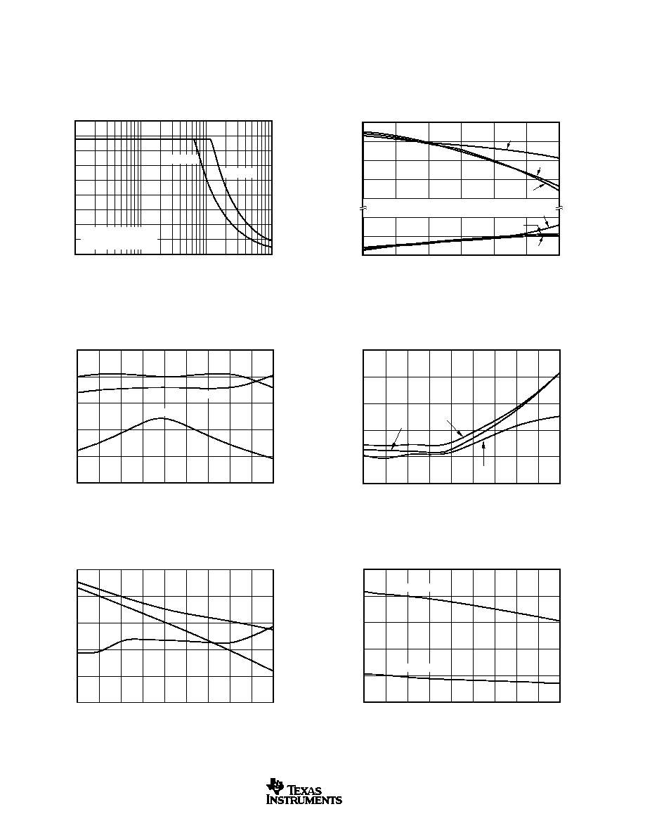
TYPICAL CHARACTERISTICS
At T
J
= +25
∞
C, V
S
=
±
40V, and R
L
= 3.8k
, unless otherwise noted.
All temperatures are junction temperatures unless otherwise noted. Refer to the Applications Information section to calculate junction temperatures from ambient
temperatures for a specific configuration.
140
120
100
80
60
40
20
0
≠20
≠40
0
≠20
≠40
≠60
≠80
≠100
≠120
≠140
≠160
≠180
1
10
100
1k
10k
100k
1M
10M
Frequency (Hz)
Gain (dB)
OPEN-LOOP GAIN AND PHASE vs FREQUENCY
Phase (
∞
)
Phase
Gain
OPA452
140
120
100
80
60
40
20
0
≠20
≠40
0
≠20
≠40
≠60
≠80
≠100
≠120
≠140
≠160
≠180
1
10
100
1k
10k
100k
1M
10M
Frequency (Hz)
Gain (dB)
OPEN-LOOP GAIN AND PHASE vs FREQUENCY
Phase (
∞
)
Phase
OPA453
Gain
120
100
80
60
40
20
0
1
10
100
1k
10k
100k
1M
10M
Frequency (Hz)
CMRR (dB)
COMMON-MODE REJECTION RATIO vs FREQUENCY
140
120
100
80
60
40
20
1
10
100
1k
10k
100k
1M
10M
Frequency (Hz)
PSRR (dB)
POWER-SUPPLY REJECTION RATIO vs FREQUENCY
≠PSRR
+PSRR
100
10
1
INPUT VOLTAGE AND CURRENT NOISE
SPECTRAL DENSITY vs FREQUENCY
Voltage Noise (nV/
Hz)
Current Noise (fA/
Hz)
10
100
1k
10k
100k
1M
Frequency (Hz)
i
n
e
n
1
0.1
0.01
0.001
0.0001
TOTAL HARMONIC DISTORTION + NOISE
vs FREQUENCY
Frequency (Hz)
10
100
1k
10k
100k
THD+N (%)
A
V
= +5
V
O
= 30Vp-p
R
L
= 600
, 2k
OPA452
600
2k
OPA453
600
2k
OPA452, 453
6
SBOS127C
www.ti.com
TYPICAL CHARACTERISTICS
(Cont.)
At T
J
= +25
∞
C, V
S
=
±
40V, and R
L
= 3.8k
, unless otherwise noted.
All temperatures are junction temperatures unless otherwise noted. Refer to the Applications Information section to calculate junction temperatures from ambient
temperatures for a specific configuration.
45
40
35
30
25
20
15
10
5
0
1k
10k
100k
1M
Frequency (Hz)
Maximum Output Voltage (Vp-p)
MAXIMUM OUTPUT VOLTAGE SWING
vs FREQUENCY
Without Slew-Induced
Distortion
OPA452
OPA453
OUTPUT VOLTAGE SWING vs OUTPUT CURRENT
(V+)
(V+) ≠ 2
(V+) ≠ 4
(V+) ≠ 6
(V≠) ≠ 8
(V≠) + 4
(V≠) + 2
(V≠)
0
20
40
60
80
100
120
Output Current (mA)
Output Voltage Swing (V)
+85
∞
C
+25
∞
C
+25
∞
C
≠55
∞
C
+85
∞
C
≠55
∞
C
160
140
120
100
80
60
≠55
≠35
≠15
5
25
65
45
85
105
125
Temperature (
∞
C)
Short-Circuit Current (mA)
5.7
5.5
5.3
QUIESCENT CURRENT AND SHORT-CIRCUIT
CURRENT vs TEMPERATURE
+I
SC
≠I
SC
I
Q
Quiescent Current (mA)
10
8
6
4
2
0
≠55
≠35
≠15
5
25
65
45
85
105
125
Temperature (
∞
C)
Gain Bandwidth (MHz)
GAIN BANDWIDTH PRODUCT
vs TEMPERATURE
OPA453
OPA452
120
110
100
90
80
70
≠55
≠35
≠15
5
25
65
45
85
105
125
Temperature (
∞
C)
AOL, PSRR, and CMRR (dB)
OPEN-LOOP GAIN, POWER-SUPPLY
REJECTION RATIO, AND COMMON-MODE
REJECTION RATIO vs TEMPERATURE
AOL
PSRR
CMRR
10000
1000
100
10
1
0.1
≠55
≠35
≠15
5
25
65
45
85
105
125
Temperature (
∞
C)
Current (pA)
INPUT BIAS CURRENT AND INPUT
OFFSET CURRENT vs TEMPERATURE
≠I
B
I
OS
+I
B
OPA452, 453
7
SBOS127C
www.ti.com
TYPICAL CHARACTERISTICS
(Cont.)
At T
J
= +25
∞
C, V
S
=
±
40V, and R
L
= 3.8k
, unless otherwise noted.
All temperatures are junction temperatures unless otherwise noted. Refer to the Applications Information section to calculate junction temperatures from ambient
temperatures for a specific configuration.
20
15
10
5
0
≠5
≠40
≠30
≠20
≠10
0
30
20
10
40
Common-Mode Voltage (V)
Current (pA)
INPUT BIAS CURRENT AND INPUT OFFSET CURRENT
vs COMMON-MODE VOLTAGE
+I
B
≠I
B
I
OS
15
10
5
0
≠3
≠2
≠1
0
1
2
3
Offset Voltage (mV)
Percentage of Amplifiers (%)
OFFSET VOLTAGE
PRODUCTION DISTRIBUTION
45
35
25
15
5
≠55
≠35
≠15
5
25
45
65
85
105
125
Temperature (
∞
C)
Slew Rate (V/
µ
s)
SLEW RATE vs TEMPERATURE
≠Slew (OPA453)
+Slew (OPA453)
≠Slew (OPA452)
+Slew (OPA452)
100
10
1
1
10
100
Gain (V/V)
Settling Time (
µ
s)
SETTLING TIME vs CLOSED-LOOP GAIN
0.01%
OPA452
OPA453
0.01%
0.1%
0.1%
20
15
10
5
0
0
1
Offset Voltage Drift (
µ
V/
∞
C)
Amplifiers (%)
OFFSET VOLTAGE DRIFT DISTRIBUTION
2
3
4
5
6
7
8
9 10 11 12 13 14 15 16 17 18
130
120
110
6
5
≠55
10
20
30
40
Temperature (
∞
C)
Short-Circuit Current (mA)
QUIESCENT CURRENT AND SHORT-CIRCUIT
CURRENT vs TEMPERATURE
+I
SC
≠I
SC
I
Q
Quiescent Current (mA)
OPA452, 453
8
SBOS127C
www.ti.com
TYPICAL CHARACTERISTICS
(Cont.)
At T
J
= +25
∞
C, V
S
=
±
40V, and R
L
= 3.8k
, unless otherwise noted.
All temperatures are junction temperatures unless otherwise noted. Refer to the Applications Information section to calculate junction temperatures from ambient
temperatures for a specific configuration.
60
50
40
30
20
10
0
0.01
0.1
1
10
32
Load Capacitance
Overshoot (%)
SMALL-SIGNAL OVERSHOOT
vs LOAD CAPACITANCE
G = +1
G = ≠6
G = ≠8
OPA452
OPA453
G = ≠1
G = ≠4
G = ≠2
LARGE-SIGNAL STEP RESPONSE
(G = 1, C
L
= 100pF)
10V/div
2.5
µ
s/div
OPA452
LARGE-SIGNAL STEP RESPONSE
(G = 5, C
L
= 100pF)
10V/div
2.5
µ
s/div
OPA453
SMALL-SIGNAL STEP RESPONSE
(G = 1, C
L
= 100pF)
20V/div
1
µ
s/div
OPA452
SMALL-SIGNAL STEP RESPONSE
(G = 5, C
L
= 100pF)
20V/div
500ns/div
OPA453
SMALL-SIGNAL STEP RESPONSE
(G = ≠1, C
L
= 1000pF)
20V/div
2.5
µ
s/div
OPA452

OPA452, 453
9
SBOS127C
www.ti.com
APPLICATIONS INFORMATION
Figure 1 shows the OPA452 connected as a basic noninverting
amplifier. The OPA452 can be used in virtually any op amp
configuration. The OPA453 is designed for use in configura-
tions with gains of 5 or greater. Power-supply terminals
should be bypassed with 0.1
µ
F capacitors, or greater, near
the power-supply pins. Be sure that the capacitors are
appropriately rated for the power-supply voltage used. The
OPA452 and OPA453 can supply output currents up to
50mA with excellent performance.
FIGURE 1. Basic Circuit Connections.
CURRENT LIMIT
The OPA452 and OPA453 are designed with internal cur-
rent-limiting circuitry that limits the output current to approxi-
mately 125mA. The current limit varies slightly with increas-
ing junction temperature and supply voltage, as shown in the
Typical Characteristics. Current limit, in combination with the
thermal protection circuitry, provides protection from most
types of overload conditions including short-circuit to ground.
THERMAL PROTECTION
The OPA452 and OPA453 have thermal shutdown circuitry
that protects the amplifier from damage caused by overload
conditions. The thermal protection circuitry disables the out-
put when the junction temperature reaches approximately
160
∞
C, allowing the device to cool. When the junction tem-
perature cools to approximately 140
∞
C, the output circuitry is
automatically re-enabled.
The thermal shutdown function is not intended to replace
proper heat sinking. Activation of the thermal shutdown
circuitry is an indication of excessive power dissipation or an
inadequate heat sink. Continuously running the amplifier into
thermal shutdown can degrade reliability.
The Thermal Shutdown Indicator (Flag) pin can be monitored
to determine if shutdown is occurring. During normal opera-
tion, the current output from the flag pin is typically 50nA.
During shutdown, the current output from the flag pin in-
creases to 140
µ
A (typical). This current output allows for
easy interfacing to external logic. Figure 2 shows two ex-
amples implementing this function.
FIGURE 2. Thermal Shutdown Indicator.
G = 1+
R
2
R
1
Z
L
R
2
R
1
0.1
µ
F
10
µ
F
OPA452
V≠
V+
+
+
V
IN
10
µ
F
0.1
µ
F
V
O
Flag
(optional)
Flag
100
µ
A to
165
µ
A
HCT
OPA452
Logic
Ground
V
OUT
+5V
19.1k
+5V
V
OUT
CMOS
OPA452
Logic
Ground
Interfacing with CMOS Logic
Interfacing with HCT Logic
39k
Interface to virtually any CMOS
logic gate by choosing a resistor
value that provides an assured
logic high voltage with the
minimum (100
µ
A) flag current.
HCT logic has relatively well-
controlled logic level. A properly
chosen resistor value can
assure proper logic high level
throughout the full range of flag
output current.

OPA452, 453
10
SBOS127C
www.ti.com
POWER SUPPLIES
The OPA452 and OPA453 may be operated from power
supplies of
±
10V to
±
40V, or a total of 80V with excellent
performance. Most behavior remains unchanged throughout
the full operating voltage range. Parameters that vary signifi-
cantly with operating voltage are shown in the Typical Char-
acteristics.
For applications that do not require symmetrical output volt-
age swing, power-supply voltages do not need to be equal.
The OPA452 and OPA453 can operate with as little as 20V
between the supplies or with up to 80V between the supplies.
For example, the positive supply could be set to 70V with the
negative supply at ≠10V or vice-versa.
The tabs of the DDPAK-7 and TO220 packages are electri-
cally connected to the negative supply (V≠), however, these
connections should not be used to carry current. For best
thermal performance, the tab should be soldered directly to
the circuit board copper area (see Heat Sinking section).
POWER DISSIPATION
Internal power dissipation of these op amps can be quite
large. All of the specifications for the OPA452 and OPA453
may change with junction temperature. If the device is not
subjected to internal self-heating, the junction temperature
will be the same as the ambient. However, in practical
applications, the device will self-heat and the junction tem-
perature will be significantly higher than ambient. The follow-
ing calculation can be performed to establish junction tem-
perature as a function of ambient temperature and the
conditions of the application.
Consider the OPA452 in a circuit configuration where the
load is 600
and the output voltage is 20V. The supplies are
at
±
40V and the ambient temperature (T
A
) is 40
∞
C. The
JA
for the package plus heat sink is 30
∞
C/W.
First, the quiescent heating of the op amp is as follows:
P
D(internal)
= I
Q
∑ V
S
= 6mA ∑ 80V = 480mW
The output current (I
O
) can be calculated:
I
O
= V
O
/R
L
= 20V/600
= 33.33mA
The power being dissipated (P
D
) in the output transistor of
the amplifier can be calculated:
P
D(output stage)
= I
O
∑ (V
S
≠ V
O
) = 33.3mA ∑ (40 ≠ 20) = 667mW
P
D(total)
= P
D(internal)
+ P
D(output stage)
= 480mW + 667mW = 1147mW
The resulting junction temperature can be calculated:
T
J
= T
A
+ P
D
JA
T
J
= 40
∞
C + 1147mW ∑ 30
∞
C/W = 74.4
∞
C
FIGURE 3. DDPAK-7 and TO220-7 Safe Operating Area.
Where,
V
O
= output voltage
V
S
= supply voltage
I
O
= output current
R
L
= load resistance
T
J
= junction temperature (
∞
C)
T
A
= ambient temperature (
∞
C)
JA
= junction-to-air thermal resistance (
∞
C/W)
To estimate the margin of safety in a complete design
(including heat sink), increase the ambient temperature until
the thermal protection is activated. Use worst-case load and
signal conditions. For good reliability, the thermal protection
should trigger more than +35
∞
C above the maximum ex-
pected ambient condition of your application. This ensures a
maximum junction temperature of +125
∞
C at the maximum
expected ambient condition.
Operation from a single power supply (or unbalanced power
supplies) can produce even larger power dissipation be-
cause a larger voltage can be impressed across the conduct-
ing output transistor. Consult Application Bulletin SBOA022
at www.ti.com for further information on how to calculate or
measure power dissipation.
Power dissipation can be minimized by using the lowest
possible supply voltage. For example, with a 50mA load, the
output will swing to within 5.0V of the power-supply rails.
Power supplies set to no more than 5.0V above the maxi-
mum output voltage swing required by the application will
minimize the power dissipation.
SAFE OPERATING AREA
The Safe Operating Area (SOA curves, Figure 3) shows the
permissible range of voltage and current. The safe output
current decreases as the voltage across the output transistor
(V
S
≠ V
O
) increases. For further insight on SOA, consult
Application Report SBOA022.
Output short circuits are a very demanding case for SOA. A
short-circuit to ground forces the full power-supply voltage
(V+ or V≠) across the conducting transistor and produces a
100
10
1
0.1
50
10
80
100
| V
S
| ≠ | V
O
| (V)
I
O
(mA)
SAFE OPERATING AREA
is total thermal
resistance including
junction-to-case.
This graph is for
+125
∞
C max operating
temperature.
+85
∞
C, = 20
+85
∞
C, = 40
+25
∞
C, = 40
+25
∞
C, = 3

OPA452, 453
11
SBOS127C
www.ti.com
typical output current of 125mA. With
±
40V power supplies,
this creates an internal dissipation of 10W. This far exceeds
practical heat sinking and is not recommended. If operation
in this region is unavoidable, use the part with a heat sink.
HEAT SINKING
Power dissipated in the OPA452 or OPA453 will cause the
junction temperature to rise. For reliable operation, the junc-
tion temperature should be limited to +125
∞
C. Many applica-
tions will require a heat sink to assure that the maximum
operating junction temperature is not exceeded. The heat
sink required depends on the power dissipated and on
ambient conditions.
For heat sinking purposes, the tab of the DDPAK is typically
soldered directly to a circuit board copper area. Increasing
the copper area improves heat dissipation. Figure 4 shows
typical thermal resistance from junction-to-ambient as a
function of copper area.
Depending on conditions, additional heat sinking may be
required. Aavid Thermal Products Inc. manufactures sur-
face-mountable heat sinks designed specifically for use with
these packages. Further information is available on Aavid's
web site, www.aavid.com.
FIGURE 4. DDPAK Thermal Resistance versus Circuit Board
Copper Area.
CAPACITIVE LOADS
The dynamic characteristics of the OPA452 and OPA453
have been optimized for commonly encountered gains, loads,
and operating conditions. The combination of low closed-
loop gain and capacitive load will decrease the phase margin
and may lead to gain peaking or oscillations. Figure 5 shows
a circuit that preserves phase margin with capacitive load.
Figure 6 shows the small-signal step response for the circuit
in Figure 5. Consult Application Bulletin SBOA015, at
www.ti.com, for more information.
FIGURE 5. Driving Large Capacitive Loads.
R
F
5k
C
S
1.8nF
10nF
OPA452
+40V
≠40V
V
I
C
F
270pF
R
G
5k
THERMAL RESISTANCE vs
CIRCUIT BOARD COPPER AREA
50
40
30
20
10
0
0
1
2
3
4
5
Copper Area (inches
2
)
OPA452FA, OPA453FA
Surface-Mount Package
1oz. copper
Circuit Board Copper Area
OPA452FA, OPA453FA
Surface-Mount Package
Thermal Resistance,
JA
(
∞
C/W)
FIGURE 6. Small-Signal Step Response for Figure 5.
SMALL-SIGNAL STEP RESPONSE
(G = ≠1, C
L
= 10nF)
20mV/div
2.5
µ
s/div
OPA452

OPA452, 453
12
SBOS127C
www.ti.com
INCREASING OUTPUT CURRENT
In those applications where the 50mA of output current is not
sufficient to drive the desired load, output current can be
increased by connecting two or more OPA452s or OPA453s
in parallel, as shown in Figure 7. Amplifier A1 is the master
amplifier and may be configured in virtually any op amp
circuit. Amplifier A2, the slave, is configured as a unity gain
buffer. Alternatively, external output transistors can be used
to boost output current. The circuit in Figure 8 is capable of
supplying output currents up to 1A. Alternatively, the OPA547,
OPA548, and OPA549 series power op amps should be
considered for high output current drive, along with program-
mable current limit and output disable capability.
FIGURE 7. Parallel Amplifiers Increase Output Current Ca-
pability.
INPUT PROTECTION
The OPA452 and OPA453 feature internal clamp diodes to
protect the inputs when voltages beyond the supply rails are
encountered. However, input current should be limited to
5mA. In some cases, an external series resistor may be
required. Many input signals are inherently current-limited,
therefore, a limiting resistor may not be required. Please
consider that a large series resistor, in conjunction with the
input capacitance, can affect stability.
USING THE OPA453 IN LOW GAINS
The OPA453 is intended for applications with signal gains of
5 or greater, but it is possible to take advantage of its high
slew rate in lower gains using an external compensation
technique in an inverting configuration. This technique main-
tains low noise characteristics of the OPA453 architecture at
low frequencies. Depending on the application, a small in-
crease in high-frequency noise may result. This technique
shapes the loop gain for good stability while giving an easily
controlled 2nd-order low-pass frequency response.
Considering only the noise gain (noninverting signal gain) for
the circuit of Figure 9, the low-frequency noise gain (NG
1
) will
be set by the resistor ratios, whereas the high-frequency
noise gain (NG
2
) will be set by the capacitor ratios. The
capacitor values set both the transition frequencies and the
high-frequency noise gain. If this noise gain, determined by
NG
2
= 1 + C
S
/C
F
, is set to a value greater than the recom-
mended minimum stable gain for the op amp and the noise
gain pole, set by 1/R
F
C
F
, is placed correctly, a very well
controlled, 2nd-order low-pass frequency response will result.
To choose the values for both C
S
and C
F
, two parameters
and only three equations need to be solved. First, the target
for the high-frequency noise gain (NG
2
) should be greater
than the minimum stable gain for the OPA453. In the circuit
in Figure 9, a target NG
2
of 10 is used. Second, the signal
gain of ≠1 in Figure 10 sets the low-frequency noise gain to
NG
1
= 1 + R
F
/R
G
(= 2 in this example). Using these two gains,
knowing the Gain Bandwidth Product (GBP) for the OPA453
(7.5MHz), and targeting a maximally flat 2nd-order, low-pass
Butterworth frequency response (Q = 0.707), the key fre-
quency in the compensation can be found.
For the values in Figure 9, the f
≠3dB
will be approximately
180kHz. This is less than that predicted by simply dividing the
GBP by NG
1
. The compensation network controls the band-
width to a lower value while providing good slew rate at the
output and an exceptional distortion performance due to
increased loop gain at frequencies below NG
1
∑ Z
0
. The
capacitor values in Figure 10 are calculated for NG
1
= 2 and
NG
2
= 10 with no adjustment for parasitics.
Actual circuit values can be optimized by checking the small-
signal step response with actual load conditions. See Figure 9
for the small-signal step response of this OPA453, G = ≠1
circuit with a 1000pF load. It is well-behaved with no tendency
to oscillate. If C
S
and C
F
were removed, the circuit would be
unstable.
FIGURE 8. External Output Transistors Boost Output Cur-
rent Up to 1 Amp.
R
1
R
2
OPA452
OPA452
"SLAVE"
"MASTER"
V
IN
R
S
(1)
10
R
S
(1)
10
R
L
NOTE: (1) R
S
resistors minimize the circulating
current that can flow between the two devices
due to V
OS
errors.
R
1
R
2
OPA452
TIP30C
TIP29C
V
IN
+40V
≠40V
V
O
R
3
(1)
100
NOTE: (1) R
3
provides current limit and allows the amplifier to
drive the load when the output is between 0.7V and ≠0.7V.
R
4
0.2
R
4
0.2
LOAD
C
F

OPA452, 453
13
SBOS127C
www.ti.com
FIGURE 9. Compensation of the OPA453 for G = ≠1.
FIGURE 10. Small-Signal Step Response for Figure 9.
R
F
5k
C
S
1.8nF
NG
1
= 1 + R
F
/R
G
= 2
NG
2
= 1 + C
S
/C
F
= 10
OPA453
+40V
≠40V
V
IN
V
OUT
C
F
200pF
R
G
5k
SMALL-SIGNAL STEP RESPONSE
(G = ≠1, C
L
= 1000pF)
20mV/div
2.5
µ
s/div
OPA453

PACKAGING INFORMATION
ORDERABLE DEVICE
STATUS(1)
PACKAGE TYPE
PACKAGE DRAWING
PINS
PACKAGE QTY
OPA452FA
OBSOLETE
PFM
KTW
7
OPA452FA/500
ACTIVE
PFM
KTW
7
500
OPA452FAKTWT
ACTIVE
PFM
KTW
7
50
OPA452FKTWT
ACTIVE
PFM
KTW
7
50
OPA452TA
ACTIVE
TO/SOT
KC
7
49
OPA452TA-1
ACTIVE
TO/SOT
KC
7
49
OPA453FA
OBSOLETE
PFM
KTW
7
OPA453FA/500
ACTIVE
PFM
KTW
7
500
OPA453FAKTWT
ACTIVE
PFM
KTW
7
50
OPA453FKTWT
ACTIVE
PFM
KTW
7
50
OPA453TA
ACTIVE
TO/SOT
KC
7
49
OPA453TA-1
ACTIVE
TO/SOT
KC
7
49
(1) The marketing status values are defined as follows:
ACTIVE: Product device recommended for new designs.
LIFEBUY: TI has announced that the device will be discontinued, and a lifetime-buy period is in effect.
NRND: Not recommended for new designs. Device is in production to support existing customers, but TI does not recommend using this part in
a new design.
PREVIEW: Device has been announced but is not in production. Samples may or may not be available.
OBSOLETE: TI has discontinued the production of the device.
PACKAGE OPTION ADDENDUM
www.ti.com
12-Nov-2003

MECHANICAL DATA
MPSF015 ≠ AUGUST 2001
POST OFFICE BOX 655303
∑
DALLAS, TEXAS 75265
KTW (R-PSFM-G7)
PLASTIC FLANGE-MOUNT
0.010 (0,25)
A
M
4201284/A 08/01
0.385 (9,78)
0.410 (10,41)
M
M
B
C
≠A≠
0.006
≠B≠
0.170 (4,32)
0.183 (4,65)
0.000 (0,00)
0.012 (0,305)
0.104 (2,64)
0.096 (2,44)
0.034 (0,86)
0.022 (0,57)
0.050 (1,27)
0.055 (1,40)
0.045 (1,14)
0.014 (0,36)
0.026 (0,66)
0.330 (8,38)
0.370 (9,40)
0.297 (7,54)
0.303 (7,70)
0.0585 (1,485)
0.0625 (1,587)
0.595 (15,11)
0.605 (15,37)
0.019 (0,48)
0.017 (0,43)
0
∞
~3
∞
0.179 (4,55)
0.187 (4,75)
0.056 (1,42)
0.064 (1,63)
0.296 (7,52)
0.304 (7,72)
0.300 (7,62)
0.252 (6,40)
F
C
C
H
H
H
C
A
NOTES: A. All linear dimensions are in inches (millimeters).
B. This drawing is subject to change without notice.
C. Lead width and height dimensions apply to the
plated lead.
D. Leads are not allowed above the Datum B.
E. Stand≠off height is measured from lead tip
with reference to Datum B.
F. Lead width dimension does not include dambar
protrusion. Allowable dambar protrusion shall not
cause the lead width to exceed the maximum
dimension by more than 0.003".
G. Cross≠hatch indicates exposed metal surface.
H. Falls within JEDEC MO≠169 with the exception
of the dimensions indicated.

MECHANICAL DATA
MSOT010 ≠ OCTOBER 1994
1
POST OFFICE BOX 655303
∑
DALLAS, TEXAS 75265
KC (R-PSFM-T7)
PLASTIC FLANGE-MOUNT PACKAGE
4040251 / B 01/95
0.420 (10,67)
0.055 (1,40)
0.335 (8,51)
0.030 (0,76)
0.026 (0,66)
0.380 (9,65)
0.325 (8,25)
0.045 (1,14)
0.113 (2,87)
0.103 (2,62)
0.146 (3,71)
0.156 (3,96)
0.122 (3,10)
0.102 (2,59)
DIA
(see Note C)
0.125 (3,18)
0.137 (3,48)
0.147 (3,73)
1.020 (25,91)
1.000 (25,40)
0.175 (4,46)
0.185 (4,70)
1
7
0.050 (1,27)
0.300 (7,62)
0.025 (0,64)
0.012 (0,30)
M
0.010 (0,25)
NOTES: A. All linear dimensions are in inches (millimeters).
B. This drawing is subject to change without notice.
C. Lead dimensions are not controlled within this area.
D. All lead dimensions apply before solder dip.
E. The center lead is in electrical contact with the mounting tab.

IMPORTANT NOTICE
Texas Instruments Incorporated and its subsidiaries (TI) reserve the right to make corrections, modifications,
enhancements, improvements, and other changes to its products and services at any time and to discontinue
any product or service without notice. Customers should obtain the latest relevant information before placing
orders and should verify that such information is current and complete. All products are sold subject to TI's terms
and conditions of sale supplied at the time of order acknowledgment.
TI warrants performance of its hardware products to the specifications applicable at the time of sale in
accordance with TI's standard warranty. Testing and other quality control techniques are used to the extent TI
deems necessary to support this warranty. Except where mandated by government requirements, testing of all
parameters of each product is not necessarily performed.
TI assumes no liability for applications assistance or customer product design. Customers are responsible for
their products and applications using TI components. To minimize the risks associated with customer products
and applications, customers should provide adequate design and operating safeguards.
TI does not warrant or represent that any license, either express or implied, is granted under any TI patent right,
copyright, mask work right, or other TI intellectual property right relating to any combination, machine, or process
in which TI products or services are used. Information published by TI regarding third-party products or services
does not constitute a license from TI to use such products or services or a warranty or endorsement thereof.
Use of such information may require a license from a third party under the patents or other intellectual property
of the third party, or a license from TI under the patents or other intellectual property of TI.
Reproduction of information in TI data books or data sheets is permissible only if reproduction is without
alteration and is accompanied by all associated warranties, conditions, limitations, and notices. Reproduction
of this information with alteration is an unfair and deceptive business practice. TI is not responsible or liable for
such altered documentation.
Resale of TI products or services with statements different from or beyond the parameters stated by TI for that
product or service voids all express and any implied warranties for the associated TI product or service and
is an unfair and deceptive business practice. TI is not responsible or liable for any such statements.
Following are URLs where you can obtain information on other Texas Instruments products and application
solutions:
Products
Applications
Amplifiers
amplifier.ti.com
Audio
www.ti.com/audio
Data Converters
dataconverter.ti.com
Automotive
www.ti.com/automotive
DSP
dsp.ti.com
Broadband
www.ti.com/broadband
Interface
interface.ti.com
Digital Control
www.ti.com/digitalcontrol
Logic
logic.ti.com
Military
www.ti.com/military
Power Mgmt
power.ti.com
Optical Networking
www.ti.com/opticalnetwork
Microcontrollers
microcontroller.ti.com
Security
www.ti.com/security
Telephony
www.ti.com/telephony
Video & Imaging
www.ti.com/video
Wireless
www.ti.com/wireless
Mailing Address:
Texas Instruments
Post Office Box 655303 Dallas, Texas 75265
Copyright
2003, Texas Instruments Incorporated