 | –≠–ª–µ–∫—Ç—Ä–æ–Ω–Ω—ã–π –∫–æ–º–ø–æ–Ω–µ–Ω—Ç: OPA548T-1 | –°–∫–∞—á–∞—Ç—å:  PDF PDF  ZIP ZIP |
Document Outline
- FEATURES
- APPLICATIONS
- DESCRIPTION
- ABSOLUTE MAXIMUM RATINGS(1)
- PACKAGE/ORDERING INFORMATION
- PIN CONFIGURATIONS
- ELECTRICAL CHARACTERISTICS
- TYPICAL CHARACTERISTICS
- APPLICATIONS INFORMATION
- POWER SUPPLIES
- ADJUSTABLE CURRENT LIMIT
- SAFE OPERATING AREA
- AMPLIFIER MOUNTING
- POWER DISSIPATION
- THERMAL PROTECTION
- HEAT SINKING
- Heat Sink Selection Example
- ENABLE/STATUS (E/S) PIN
- Output Disable
- Thermal Shutdown Status
- Output Disable and Thermal Shutdown Status
- OUTPUT STAGE COMPENSATION
- OUTPUT PROTECTION
- VOLTAGE SOURCE APPLICATION
- PROGRAMMABLE POWER SUPPLY

OPA548
V
IN
≠
V
IN
+
V+
E/S
R
CL
R
CL
sets the current limit
value from 0 to 5A.
(1/4W Resistor)
I
LIM
V
O
V≠
High-Voltage, High-Current
OPERATIONAL AMPLIFIER
DESCRIPTION
The OPA548 is a low-cost, high-voltage/high-current opera-
tional amplifier ideal for driving a wide variety of loads. A
laser-trimmed monolithic integrated circuit provides excellent
low-level signal accuracy and high output voltage and cur-
rent.
The OPA548 operates from either single or dual supplies for
design flexibility. In single-supply operation, the input com-
mon-mode range extends below ground.
The OPA548 is internally protected against over-temperature
conditions and current overloads. In addition, the OPA548
was designed to provide an accurate, user-selected current
limit. Unlike other designs which use a "power" resistor in
series with the output current path, the OPA548 senses the
load indirectly. This allows the current limit to be adjusted
from 0A to 5A with a resistor/potentiometer or controlled
digitally with a voltage-out or current-out DAC.
The Enable/Status (E/S) pin provides two functions. An input
on the pin not only disables the output stage to effectively
disconnect the load, but also reduces the quiescent current
to conserve power. The E/S pin output can be monitored to
determine if the OPA548 is in thermal shutdown.
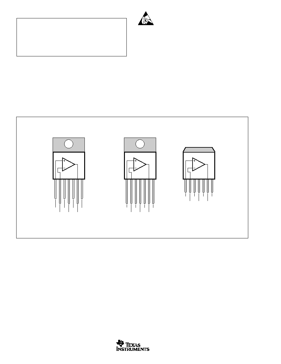
The OPA548 is available in an industry-standard
7-lead staggered and straight lead TO-220 package, and a
7-lead DDPAK surface-mount plastic power package. The
copper tab allows easy mounting to a heat sink or circuit
board for excellent thermal performance. It is specified for
operation over the extended industrial temperature range,
≠40
∞
C to +85
∞
C. A SPICE macromodel is available for
design analysis.
FEATURES
q
WIDE SUPPLY RANGE
Single Supply: +8V to +60V
Dual Supply:
±
4V to
±
30V
q
HIGH OUTPUT CURRENT:
3A Continuous
5A Peak
q
WIDE OUTPUT VOLTAGE SWING
q
FULLY PROTECTED:
Thermal Shutdown
Adjustable Current Limit
q
OUTPUT DISABLE CONTROL
q
THERMAL SHUTDOWN INDICATOR
q
HIGH SLEW RATE: 10V/
µ
s
q
LOW QUIESCENT CURRENT
q
PACKAGES:
7-Lead TO-220, Zip and Straight Leads
7-Lead DDPAK Surface-Mount
APPLICATIONS
q
VALVE, ACTUATOR DRIVERS
q
SYNCHRO, SERVO DRIVERS
q
POWER SUPPLIES
q
TEST EQUIPMENT
q
TRANSDUCER EXCITATION
q
AUDIO AMPLIFIERS
OPA548
SBOS070B ≠ OCTOBER 1997 ≠ OCTOBER 2003
www.ti.com
PRODUCTION DATA information is current as of publication date.
Products conform to specifications per the terms of Texas Instruments
standard warranty. Production processing does not necessarily include
testing of all parameters.
Copyright © 1997-2003, Texas Instruments Incorporated
Please be aware that an important notice concerning availability, standard warranty, and use in critical applications of
Texas Instruments semiconductor products and disclaimers thereto appears at the end of this data sheet.
OPA5
48
OPA
548
OPA5
48
OPA548
2
SBOS070B
www.ti.com
ABSOLUTE MAXIMUM RATINGS
(1)
Output Current ................................................................. See SOA Curve
Supply Voltage, V+ to V≠ ................................................................... 60V
Input Voltage .................................................. (V≠) ≠ 0.5V to (V+) + 0.5V
Input Shutdown Voltage ........................................................................ V+
Operating Temperature .................................................. ≠40
∞
C to +125
∞
C
Storage Temperature ..................................................... ≠55
∞
C to +125
∞
C
Junction Temperature ...................................................................... 150
∞
C
Lead Temperature (soldering 10s)
(2)
.............................................. 300
∞
C
Top Front View
PIN CONFIGURATIONS
NOTES: (1) Stresses above these ratings may cause permanent damage.
(2) Vapor-phase or IR reflow techniques are recommended for soldering the
OPA547F surface-mount package. Wave soldering is not recommended due to
excessive thermal shock and "shadowing" of nearby devices.
PACKAGE/ORDERING INFORMATION
For the most current package and ordering information, see the Package Ordering Addendum at the end of this data sheet.
ELECTROSTATIC
DISCHARGE SENSITIVITY
This integrated circuit can be damaged by ESD. Texas Instru-
ments recommends that all integrated circuits be handled with
appropriate precautions. Failure to observe proper handling
and installation procedures can cause damage.
ESD damage can range from subtle performance degradation
to complete device failure. Precision integrated circuits may be
more susceptible to damage because very small parametric
changes could cause the device not to meet its published
specifications.
7-Lead
Straight-Formed
TO-220 (T-1)
NOTE: Tabs are electrically connected to the V≠ supply.
I
LIM
V≠
V
O
V+
V
IN≠
V
IN+
1 2 3 4 5 6
E/S
7
7-Lead
DDPAK (FA)
Surface-Mount
I
LIM
V≠
V
O
V+
V
IN≠
V
IN+
1 2 3 4 5 6
E/S
7
7-Lead
Stagger-Formed
TO-220 (T)
I
LIM
V≠
V
O
V+
V
IN≠
V
IN+
1 2 3 4 5 6
E/S
7

OPA548
3
SBOS070B
www.ti.com
ELECTRICAL CHARACTERISTICS
At T
CASE
= +25
∞
C, V
S
=
±
30V and E/S pin open, unless otherwise noted.
OPA548T, F
PARAMETER
CONDITION
MIN
TYP
MAX
UNITS
OFFSET VOLTAGE
Input Offset Voltage
V
CM
= 0, I
O
= 0
±
2
±
10
mV
vs Temperature
T
A
= ≠40
∞
C to +85
∞
C
±
30
µ
V/
∞
C
vs Power Supply
V
S
=
±
4V to
±
30V
30
100
µ
V/V
INPUT BIAS CURRENT
(1)
Input Bias Current
(2)
V
CM
= 0V
≠100
≠500
nA
vs Temperature
T
A
= ≠40
∞
C to +85
∞
C
±
0.5
nA/
∞
C
Input Offset Current
V
CM
= 0V
±
5
±
50
nA
NOISE
Input Voltage Noise Density, f = 1kHz
90
nV/
Hz
Current Noise Density, f = 1kHz
200
fA/
Hz
INPUT VOLTAGE RANGE
Common-Mode Voltage Range: Positive
Linear Operation
(V+) ≠ 3
(V+) ≠ 2.3
V
Negative
Linear Operation
(V≠) ≠ 0.1
(V≠) ≠ 0.2
V
Common-Mode Rejection
V
CM
= (V≠) ≠0.1V to (V+) ≠3V
80
95
dB
INPUT IMPEDANCE
Differential
10
7
|| 6
|| pF
Common-Mode
10
9
|| 4
|| pF
OPEN-LOOP GAIN
Open-Loop Voltage Gain
V
O
=
±
25V, R
L
= 1k
90
98
dB
V
O
=
±
25V, R
L
= 8
90
dB
FREQUENCY RESPONSE
Gain-Bandwidth Product
R
L
= 8
1
MHz
Slew Rate
G = 1, 50Vp-p, R
L
= 8
10
V/
µ
s
Full-Power Bandwidth
See Typical Characteristics
kHz
Settling Time:
±
0.1%
G = ≠10, 50V Step
15
µ
s
Total Harmonic Distortion + Noise, f = 1kHz
R
L
= 8
, G = +3, Power = 10W
0.02
(3)
%
OUTPUT
Voltage Output, Positive
I
O
= 3A
(V+) ≠ 4.1
(V+) ≠ 3.7
V
Negative
I
O
= ≠3A
(V≠) + 3.7
(V≠) + 3.3
V
Positive
I
O
= 0.6A
(V+) ≠ 2.4
(V+) ≠ 2.1
V
Negative
I
O
= ≠0.6A
(V≠) + 1.3
(V≠) + 1.0
V
Maximum Continuous Current Output: dc
±
3
A
ac
3
Arms
Leakage Current, Output Disabled, dc
See Typical Characteristics
Output Current Limit
Current Limit Range
0 to
±
5
A
Current Limit Equation
I
LIM
= (15000)(4.75)/(13750
+ R
CL
)
A
Current Limit Tolerance
(1)
R
CL
= 14.8k
(I
LIM
=
±
2.5A),
±
100
±
250
mA
R
L
= 8
Capacitive Load Drive
See Typical Characteristics
(4)
OUTPUT ENABLE /STATUS (E/S) PIN
Shutdown Input Mode
V
E/S
HIGH (output enabled)
E/S Pin Open or Forced High
(V≠) + 2.4
V
V
E/S
LOW (output disabled)
E/S Pin Forced Low
(V≠) + 0.8
V
I
E/S
HIGH (output enabled)
E/S Pin High
≠65
µ
A
I
E/S
LOW (output disabled)
E/S Pin Low
≠70
µ
A
Output Disable Time
1
µ
s
Output Enable Time
3
µ
s
Thermal Shutdown Status Output
Normal Operation
Sourcing 20
µ
A
(V≠) + 2.4
(V≠) + 3.5
V
Thermally Shutdown
Sinking 5
µ
A, T
J
> 160
∞
C
(V≠) + 0.35
(V≠) + 0.8
V
Junction Temperature, Shutdown
+160
∞
C
Reset from Shutdown
+140
∞
C
POWER SUPPLY
Specified Voltage
±
30
V
Operating Voltage Range
±
4
±
30
V
Quiescent Current
I
LIM
Connected to V≠, I
O
= 0
±
17
±
20
mA
Quiescent Current, Shutdown Mode
I
LIM
Connected to V≠, I
O
= 0
±
6
mA
TEMPERATURE RANGE
Specified Range
≠40
+85
∞
C
Operating Range
≠40
+125
∞
C
Storage Range
≠55
+125
∞
C
Thermal Resistance,
JC
7-Lead DDPAK, 7-Lead TO-220
f > 50Hz
2
∞
C/W
7-Lead DDPAK, 7-Lead TO-220
dc
2.5
∞
C/W
Thermal Resistance,
JA
7-Lead DDPAK, 7-Lead TO-220
No Heat Sink
65
∞
C/W
NOTES: (1) High-speed test at T
J
= +25
∞
C. (2) Positive conventional current flows into the input terminals. (3) See "Total Harmonic Distortion+Noise vs Frequency" in
the Typical Characteristics section for additional power levels. (4) See "Small-Signal Overshoot vs Load Capacitance" in the Typical Characteristics section.

OPA548
4
SBOS070B
www.ti.com
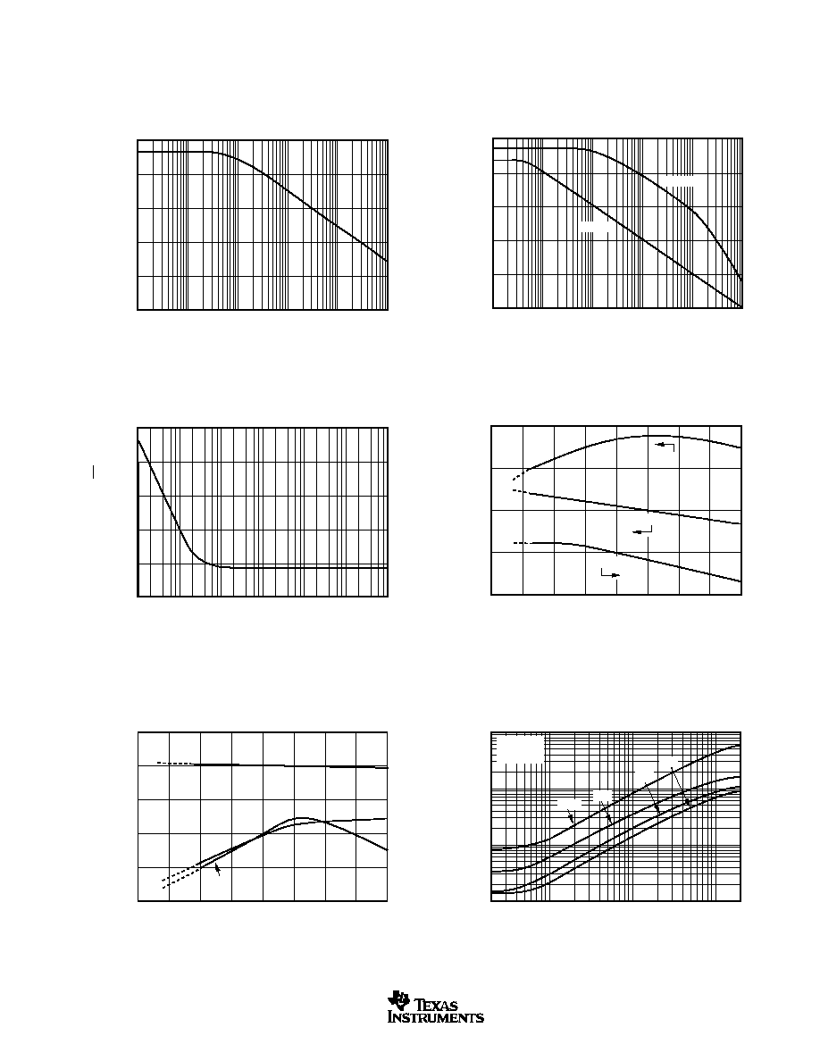
TYPICAL CHARACTERISTICS
At T
CASE
= +25
∞
C, V
S
=
±
30V and E/S pin open, unless otherwise noted.
1
10
100
1k
10k
100k
1M
10M
100
80
60
40
20
0
≠20
Gain (dB)
0
≠45
≠90
≠135
≠180
Phase (
∞
)
Frequency (Hz)
OPEN-LOOP GAIN AND PHASE
vs FREQUENCY
G
No
Load
R
L
= 8
R
L
= 8
No Load
0
±
5
±
10
±
15
±
20
±
25
±
30
±
5
±
4
±
3
±
2
±
1
0
Current Limit (A)
Supply Voltage (V)
CURRENT LIMIT vs SUPPLY VOLTAGE
R
CL
= 4.02k
R
CL
= 14.7k
R
CL
= 57.6k
≠75
≠50
≠25
0
25
50
75
100
125
≠160
≠140
≠120
≠100
≠80
≠60
≠40
Input Bias Current (nA)
Temperature (
∞
C)
INPUT BIAS CURRENT vs TEMPERATURE
V
S
=
±
5V
V
S
=
±
30V
≠30
≠20
≠10
0
10
20
30
≠200
≠150
≠100
≠50
0
Input Bias Current (nA)
Common-Mode Voltage (V)
INPUT BIAS CURRENT
vs COMMON-MODE VOLTAGE
≠75
≠50
≠25
0
25
50
75
100
125
±
20
±
18
±
16
±
14
±
12
±
10
±
8
±
6
±
4
Quiescent Current (mA)
Temperature (
∞
C)
QUIESCENT CURRENT vs TEMPERATURE
V
S
=
±
5V
I
Q
V
S
=
±
30V
V
S
=
±
5V
V
S
=
±
30V
I
Q
Shutdown
≠75
≠50
≠25
0
25
50
75
100
125
±
5
±
4
±
3
±
2
±
1
0
Current Limit (A)
Temperature (
∞
C)
CURRENT LIMIT vs TEMPERATURE
R
CL
= 4.02k
R
CL
= 14.7k
R
CL
= 57.6k
+I
LIM
≠I
LIM
OPA548
5
SBOS070B
www.ti.com
TYPICAL CHARACTERISTICS
(Cont.)
At T
CASE
= +25
∞
C, V
S
=
±
30V and E/S pin open, unless otherwise noted.
10
100
1k
10k
100k
1M
100
80
60
40
20
0
Common-Mode Rejection (dB)
Frequency (Hz)
COMMON-MODE REJECTION vs FREQUENCY
≠75
≠50
≠25
0
25
50
75
100
125
1.25
1
0.75
0.5
0.25
0
13
12
11
10
9
8
Gain-Bandwidth Product (MHz)
Slew Rate (V/
µ
s)
Temperature (
∞
C)
GAIN-BANDWIDTH PRODUCT AND
SLEW RATE vs TEMPERATURE
SR+
SR≠
GBW
1
10
100
1k
10k
100k
1M
500
400
300
200
100
0
Voltage Noise (nV/
Hz)
Frequency (Hz)
VOLTAGE NOISE DENSITY vs FREQUENCY
20
100
1k
10k
20k
1
0.1
0.01
0.001
THD+N (%)
Frequency (Hz)
TOTAL HARMONIC DISTORTION+NOISE
vs FREQUENCY
G = +3
R
L
= 8
0.1W
1W
10W
20W
10
100
1k
10k
100k
1M
100
80
60
40
20
0
Power Supply Rejection (dB)
Frequency (Hz)
POWER-SUPPLY REJECTION
vs FREQUENCY
+PSRR
≠PSRR
≠75
≠50
≠25
0
25
50
75
100
A
OL
125
100
95
90
85
80
A
OL
, PSRR (dB)
110
105
100
95
90
CMRR (dB)
Temperature (
∞
C)
OPEN-LOOP GAIN, COMMON-MODE REJECTION,
AND POWER-SUPPLY REJECTION vs TEMPERATURE
CMRR
PSRR

OPA548
6
SBOS070B
www.ti.com
TYPICAL CHARACTERISTICS
(Cont.)
At T
CASE
= +25
∞
C, V
S
=
±
30V and E/S pin open, unless otherwise noted.
0
1
2
3
4
5
4
3
2
1
0
V
SUPPLY
≠
V
OUT
(V)
Output Current (A)
OUTPUT VOLTAGE SWING vs OUTPUT CURRENT
(V+) ≠V
O
(V≠) ≠V
O
5
4
3
2
1
0
V
SUPPLY
≠
V
OUT
(V)
Temperature (
∞
C)
OUTPUT VOLTAGE SWING vs TEMPERATURE
≠75
≠50
≠25
0
25
50
75
100
125
I
O
= +3A
I
O
= ≠3A
I
O
= +0.6A
I
O
= ≠0.6A
1k
10k
100k
1M
30
25
20
15
10
5
0
Output Voltage (Vp)
Frequency (Hz)
MAXIMUM OUTPUT VOLTAGE SWING
vs FREQUENCY
Maximum Output
Voltage Without
Slew Rate Induced
Distortion
OFFSET VOLTAGE
PRODUCTION DISTRIBUTION
Percent of Amplifiers (%)
Offset Voltage (mV)
≠10 ≠9 ≠8 ≠7 ≠6 ≠5 ≠4 ≠3 ≠2 ≠1 0 1 2 3 4 5 6 7 8 9 10
20
18
16
14
12
10
8
6
4
2
0
Typical distribution
of packaged units.
OFFSET VOLTAGE DRIFT
PRODUCTION DISTRIBUTION
Percent of Amplifiers (%)
Offset Voltage Drift (
µ
V/
∞
C)
14
12
10
8
6
4
2
0
Typical production
distribution of
packaged units.
0
10
20
30
40
50
60
70
80
90 100 110 120 130
≠40
≠30
≠20
≠10
0
10
20
40
30
10
5
0
≠5
≠10
Leakage Current (mA)
Output Voltage (V)
OUTPUT LEAKAGE CURRENT
vs APPLIED OUTPUT VOLTAGE
R
L
= 8
Output Disabled
V
E/S
< (V≠) + 0.8V
R
CL
=
R
CL
= 0
OPA548
7
SBOS070B
www.ti.com
TYPICAL CHARACTERISTICS
(Cont.)
At T
CASE
= +25
∞
C, V
S
=
±
30V and E/S pin open, unless otherwise noted.
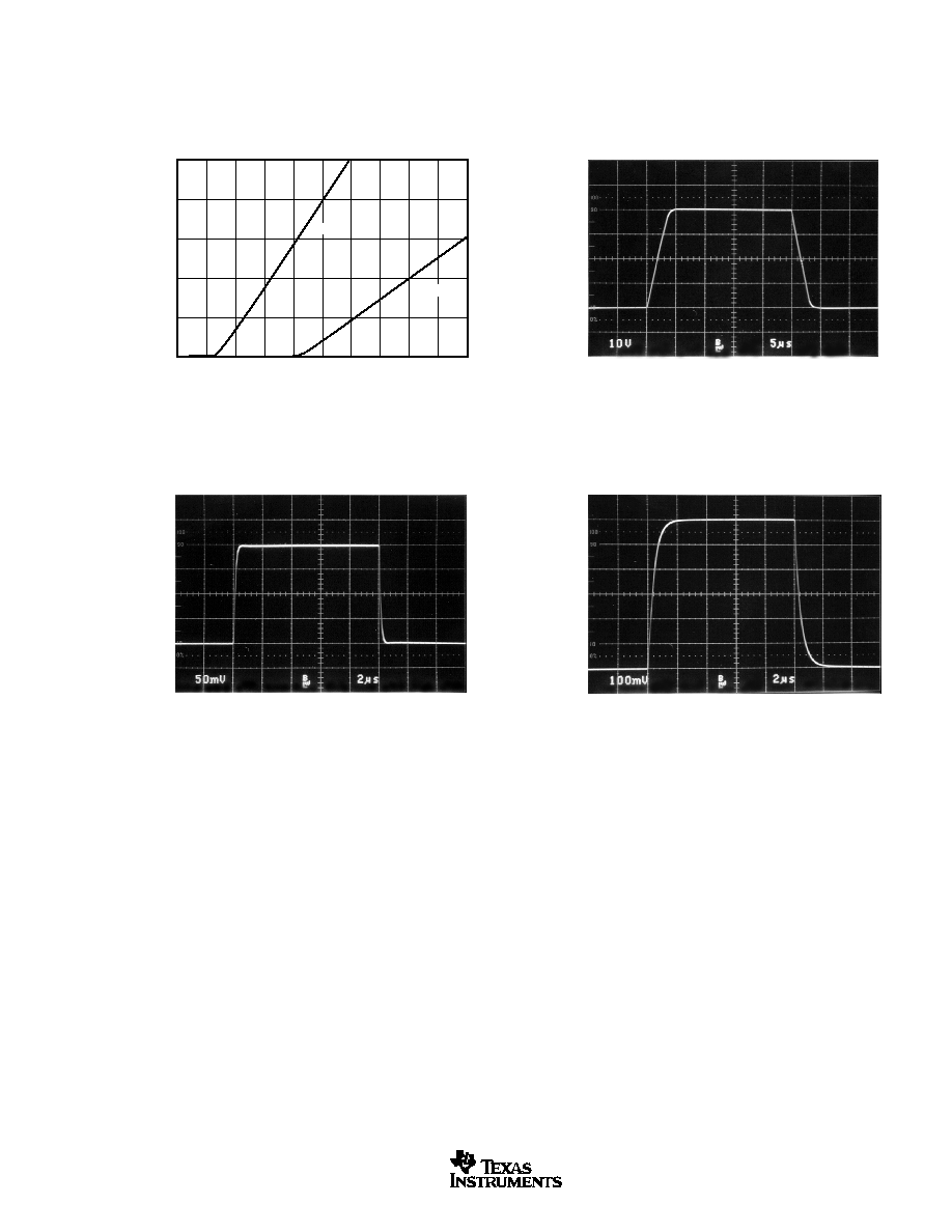
0
2k
4k
6k
8k
10k
12k
14k
16k
18k
20k
50
40
30
20
10
0
Overshoot (%)
Load Capacitance (pF)
SMALL-SIGNAL OVERSHOOT
vs LOAD CAPACITANCE
G = ≠1
G = +1
SMALL-SIGNAL STEP RESPONSE
G = 3, C
L
= 1000pF
100mV/div
2
µ
s/div
LARGE-SIGNAL STEP RESPONSE
G = 3, C
L
= 1000pF, R
L
= 8
10V/div
5
µ
s/div
SMALL-SIGNAL STEP RESPONSE
G = 1, C
L
= 1000pF
50mV/div
2
µ
s/div
OPA548
8
SBOS070B
www.ti.com
APPLICATIONS INFORMATION
Figure 1 shows the OPA548 connected as a basic noninverting
amplifier. The OPA548 can be used in virtually any op amp
configuration.
Power-supply terminals should be bypassed with low series
impedance capacitors. The technique shown in Figure 7,
using a ceramic and tantalum type in parallel is recom-
mended. In addition, we recommend a 0.01
µ
F capacitor
between V+ and V≠ as close to the OPA548 as possible.
Power-supply wiring should have low series impedance.
With the OPA548, the simplest method for adjusting the
current limit uses a resistor or potentiometer connected
between the I
LIM
pin and V≠ according to the Equation 1:
R
I
CL
LIM
=
(
)(
)
15000 4 75
13750
.
≠
The low-level control signal (0
µ
A to 330
µ
A) also allows the
current limit to be digitally controlled.
See Figure 3 for a simplified schematic of the internal
circuitry used to set the current limit. Leaving the I
LIM
pin
open programs the output current to zero, while connecting
I
LIM
directly to V≠ programs the maximum output current limit,
typically 5A.
SAFE OPERATING AREA
Stress on the output transistors is determined both by the
output current and by the output voltage across the conduct-
ing output transistor, V
S
≠ V
O
. The power dissipated by the
output transistor is equal to the product of the output current
and the voltage across the conducting transistor, V
S
≠ V
O
.
The Safe Operating Area (SOA curve, Figure 2) shows the
permissible range of voltage and current.
FIGURE 1. Basic Circuit Connections.
POWER SUPPLIES
The OPA548 operates from single (+8V to +60V) or dual
(
±
4V to
±
30V) supplies with excellent performance. Most
behavior remains unchanged throughout the full operating
voltage range. Parameters which vary significantly with oper-
ating voltage are shown in the typical characteristic curves.
Some applications do not require equal positive and negative
output voltage swing. Power-supply voltages do not need to
be equal. The OPA548 can operate with as little as 8V
between the supplies and with up to 60V between the
supplies. For example, the positive supply could be set to
55V with the negative supply at ≠5V, or vice-versa.
ADJUSTABLE CURRENT LIMIT
The OPA548 features an accurate, user-selected current
limit. Current limit is set from 0A to 5A by controlling the input
to the I
LIM
pin. Unlike other designs which use a power
resistor in series with the output current path, the OPA548
senses the load indirectly. This allows the current limit to be
set with a 0
µ
A to 330
µ
A control signal. In contrast, other
designs require a limiting resistor to handle the full output
current (5A in this case).
FIGURE 2. Safe Operating Area.
The safe output current decreases as V
S
≠ V
O
increases.
Output short-circuits are a very demanding case for SOA. A
short-circuit to ground forces the full power-supply voltage
(V+ or V≠) across the conducting transistor. Increasing the
case temperature reduces the safe output current that can be
tolerated without activating the thermal shutdown circuit of
the OPA548. For further insight on SOA, consult Application
Bulletin SBOA022.
AMPLIFIER MOUNTING
Figure 4 provides recommended solder footprints for both the
TO-220 and DDPAK power packages. The tab of both pack-
ages is electrically connected to the negative supply, V≠. It may
be desirable to isolate the tab of the TO-220 package from its
G = 1+
R
2
R
1
Z
L
E/S
3
7
5
2
1
4
6
R
2
I
LIM
(1)
R
1
0.1
µ
F
(2)
10
µ
F
OPA548
V≠
V+
+
+
V
IN
10
µ
F
0.1
µ
F
(2)
0.01
µ
F
(2)
V
O
NOTES: (1) I
LIM
connected to V≠ gives the maximum
current limit, 5A (peak). (2) Connect capacitors directly to
package power-supply pins.
1
2
5
10
V
S
≠
V
O
(V)
20
50
100
SAFE OPERATING AREA
10
1
Output Current (A)
0.1
Pulse Operation Only
(Limit rms current to
3A)
Current-Limited
Output current can
be limited to less
than 3A--see text.
T
C
= 125
∞
C
T
C
= 85
∞
C
T
C
= 25
∞
C
PD
=
5
0W
PD
=
2
6W
PD
=
1
0W
(1)
OPA548
9
SBOS070B
www.ti.com
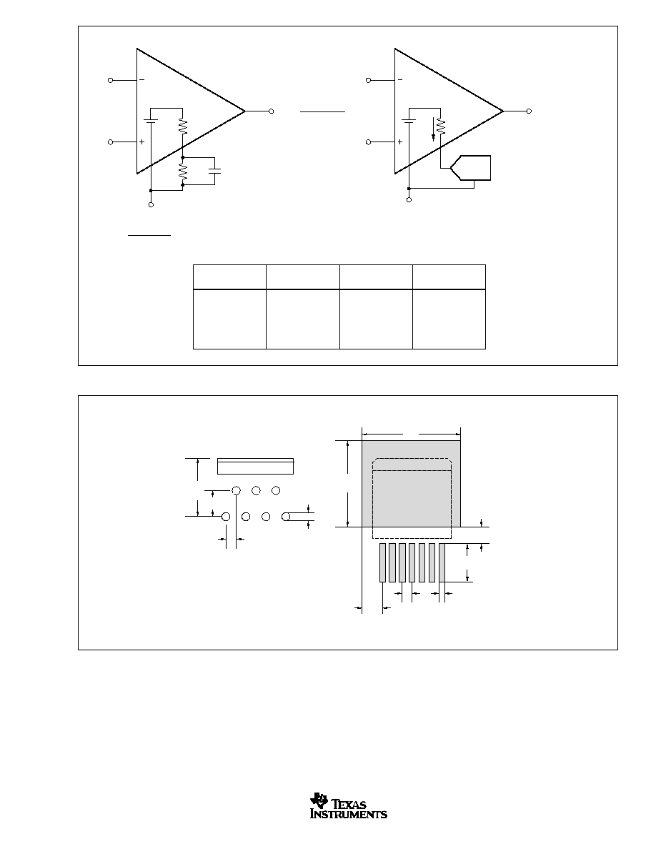
DDPAK-7
(1)
(Package Designator KTW)
TO220-7
(Package Designator KVT)
NOTE: (1) For improved thermal performance increase footprint area.
See Figure 6, "Thermal Resistance vs Circuit Board Copper Area".
Mean dimensions in inches. Refer to end of data sheet
or www.ti.com for tolerances and detailed package
drawings.
0.335
0.15
0.05
0.45
0.51
0.105
0.05
0.035
0.04
0.2
0.085
heat dissipation. See Figure 6 for typical thermal resistance
from junction-to-ambient as a function of the copper area.
POWER DISSIPATION
Power dissipation depends on power supply, signal, and load
conditions. For dc signals, power dissipation is equal to
the product of output current times the voltage across the
mounting surface with a mica (or other film) insulator (see
Figure 5). For lowest overall thermal resistance it is best to
isolate the entire heat sink/OPA548 structure from the mount-
ing surface rather than to use an insulator between the
semiconductor and heat sink.
For best thermal performance, the tab of the DDPAK sur-
face-mount version should be soldered directly to a circuit
board copper area. Increasing the copper area improves
13750
R
CL
0.01
µ
F
(optional, for noisy
environments)
3
4
3
4
4.75V
R
CL
=
≠ 13750
OPA547 CURRENT LIMIT: 0 to 5A
NOTE: (1) Resistors are nearest standard 1% values.
DESIRED
CURRENT LIMIT
0A
1A
2.5A
3A
4A
5A
RESISTOR
(1)
(R
CL
)
I
LIM
Open
57.6k
14.7k
10k
4.02k
I
LIM
Connected to V≠
CURRENT
(I
SET
)
0
µ
A
67
µ
A
167
µ
A
200
µ
A
267
µ
A
333
µ
A
VOLTAGE
(V
SET
)
(V≠) + 4.75V
(V≠) + 3.8V
(V≠) + 2.5V
(V≠) + 2V
(V≠) + 1.1V
(V≠)
RESISTOR METHOD
15000 (4.75V)
I
LIM
V≠
13750
I
SET
= I
LIM
/15000
V
SET
= (V≠) + 4.75V ≠ (13750
) (I
LIM
)/15000
DAC METHOD (Current or Voltage)
V≠
D/A
I
SET
4.75V
±
I
LIM
=
Max I
O
= I
LIM
(4.75) (15000)
13750
+ R
CL
Max I
O
= I
LIM
±
I
LIM
=15000
I
SET
FIGURE 3. Adjustable Current Limit.
FIGURE 4. TO-220 and DDPAK Solder Footprints.

OPA548
10
SBOS070B
www.ti.com
THERMAL RESISTANCE vs
CIRCUIT BOARD COPPER AREA
50
40
30
20
10
0
Thermal Resistance,
JA
(
∞
C/W)
0
1
2
3
4
5
Copper Area (inches
2
)
OPA548F
Surface Mount Package
1oz copper
Circuit Board Copper Area
OPA548
Surface-Mount Package
FIGURE 5. TO-220 Thermal Resistance vs Aluminum Plate Area.
FIGURE 6. DDPAK Thermal Resistance vs Circuit Board Copper Area.
conducting output transistor. Power dissipation can be mini-
mized by using the lowest possible power-supply voltage
necessary to assure the required output voltage swing.
For resistive loads, the maximum power dissipation occurs at
a dc output voltage of one-half the power-supply voltage.
Dissipation with ac signals is lower. Application Bulletin
SBOA022 explains how to calculate or measure power
dissipation with unusual signals and loads.
THERMAL PROTECTION
Power dissipated in the OPA548 will cause the junction
temperature to rise. The OPA548 has thermal shutdown
circuitry that protects the amplifier from damage. The thermal
protection circuitry disables the output when the junction
temperature reaches approximately 160
∞
C, allowing the de-
vice to cool. When the junction temperature cools to approxi-
mately 140
∞
C, the output circuitry is again enabled. Depend-
ing on load and signal conditions, the thermal protection
circuit may cycle on and off. This limits the dissipation of the
amplifier but may have an undesirable effect on the load.
Any tendency to activate the thermal protection circuit indi-
cates excessive power dissipation or an inadequate heat
sink. For reliable operation, junction temperature should be
limited to 125
∞
C, maximum. To estimate the margin of safety
in a complete design (including heat sink) increase the
ambient temperature until the thermal protection is triggered.
Use worst-case load and signal conditions. For good reliabil-
ity, thermal protection should trigger more than 35
∞
C above
the maximum expected ambient condition of your applica-
tion. This produces a junction temperature of 125
∞
C at the
maximum expected ambient condition.
The internal protection circuitry of the OPA548 was designed
to protect against overload conditions. It was not intended to
replace proper heat sinking. Continuously running the OPA548
into thermal shutdown will degrade reliability.
0
1
2
3
4
5
6
7
8
18
16
14
12
10
8
Thermal Resistance
JA
(
∞
C/W)
Aluminum Plate Area (inches
2
)
THERMAL RESISTANCE
vs ALUMINUM PLATE AREA
Aluminum Plate Area
Flat, Rectangular
Aluminum Plate
OPA548
TO220 Package
0.030in Al
0.062in Al
0.050in Al
Vertically Mounted
in Free Air
Optional mica or film insulator
for electrical isolation. Adds
approximately 1
∞
C/W.
Aluminum
Plate Thickness

OPA548
11
SBOS070B
www.ti.com
HEAT SINKING
Most applications require a heat sink to assure that the
maximum operating junction temperature (125
∞
C) is not
exceeded. In addition, the junction temperature should be
kept as low as possible for increased reliability. Junction
temperature can be determined according to the equation:
T
J
= T
A
+ P
D
JA
(1)
where,
JA
=
JC
+
CH
+
HA
(2)
T
J
= Junction Temperature (
∞
C)
T
A
= Ambient Temperature (
∞
C)
P
D
= Power Dissipated (W)
JC
= Junction-to-Case Thermal Resistance (
∞
C/W)
CH
= Case-to-Heat Sink Thermal Resistance (
∞
C/W)
HA
= Heat Sink-to-Ambient Thermal Resistance (
∞
C/W)
JA
= Junction-to-Air Thermal Resistance (
∞
C/W)
Figure 7 shows maximum power dissipation versus ambient
temperature with and without the use of a heat sink. Using a
heat sink significantly increases the maximum power dissipa-
tion at a given ambient temperature as shown.
The difficulty in selecting the heat sink required lies in
determining the power dissipated by the OPA548. For dc
output into a purely resistive load, power dissipation is simply
the load current times the voltage developed across the
conducting output transistor, P
D
= I
L
(V
S
≠V
O
). Other loads are
not as simple. Consult Application Bulletin SBOA022 for
further insight on calculating power dissipation. Once power
dissipation for an application is known, the proper heat sink
can be selected.
Combining equations (1) and (2) gives:
T
J
= T
A
+ P
D
(
JC
+
CH
+
HA
)
(3)
T
J
, T
A
, and P
D
are given.
JC
is provided in the specification
table, 2.5
∞
C/W (dc).
CH
can be obtained from the heat sink
manufacturer. Its value depends on heat sink size, area, and
material used. Semiconductor package type, mounting screw
torque, insulating material used (if any), and thermal
joint compound used (if any) also affect
CH
. A typical
CH
for
a TO-220 mounted package is 1
∞
C/W. Now we can solve for
HA
:
HA
J
A
D
JC
CH
HA
T
T
P
C
C
W
C W
C W
C W
=
+
(
)
=
∞
∞
∞
+ ∞
(
)
=
∞
≠
≠
≠
≠
.
/
/
.
/
125
40
5
2 5
1
13 5
To maintain junction temperature below 125
∞
C, the heat sink
selected must have a
HA
less than 14
∞
C/W. In other words,
the heat sink temperature rise above ambient must be less
than 67.5
∞
C (13.5
∞
C/W ∑ 5W). For example, at 5W Thermalloy
model number 6030B has a heat sink temperature rise of
66
∞
C above ambient (
HA
= 66
∞
C/5W = 13.2
∞
C/W), which is
below the 67.5
∞
C required in this example. Figure 7 shows
power dissipation versus ambient temperature for a TO-220
package with a 6030B heat sink.
Another variable to consider is natural convection versus
forced convection air flow. Forced-air cooling by a small fan
can lower
CA
(
CH
+
HA
) dramatically. Heat sink manufac-
tures provide thermal data for both of these cases. For
additional information on determining heat sink requirements,
consult Application Bulletin SBOA021.
As mentioned earlier, once a heat sink has been selected,
the complete design should be tested under worst-case load
and signal conditions to ensure proper thermal protection.
ENABLE/STATUS (E/S) PIN
The Enable/Status pin provides two functions: forcing this pin
LOW disables the output stage, or E/S can be monitored to
determine if the OPA548 is in thermal shutdown. One or both
of these functions can be utilized on the same device using
single or dual supplies. For normal operation (output en-
abled), the E/S pin can be left open or pulled HIGH (at least
2.4V above the negative rail). A small value capacitor con-
nected between the E/S pin and V≠ may be required for noisy
applications.
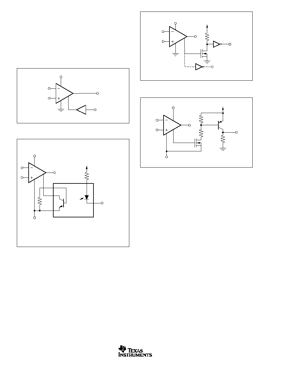
Output Disable
A unique feature of the OPA548 is its output disable capabil-
ity. This function not only conserves power during idle peri-
ods (quiescent current drops to approximately 6mA), but also
allows multiplexing in low frequency (f < 20kHz), multichan-
nel applications. Signals greater than 20kHz may cause
leakage current to increase in devices that are shutdown.
Figure 18 shows the two OPA548s in a switched amplifier
configuration. The on/off state of the two amplifiers is con-
trolled by the voltage on the E/S pin.
Heat Sink Selection Example
A TO-220 package is dissipating 5W. The maximum ex-
pected ambient temperature is 40
∞
C. Find the proper heat
sink to keep the junction temperature below 125
∞
C (150
∞
C
minus 25
∞
C safety margin).
FIGURE 7. Maximum Power Dissipation vs Ambient
Temperature.
10
8
6
4
2
0
Power Dissipation (Watts)
0
25
50
75
100
125
Ambient Temperature (
∞
C)
MAXIMUM POWER DISSIPATION
vs AMBIENT TEMPERATURE
TO220 with Thermalloy
6030B Heat Sink
JA
= 16.7
∞
C/W
P
D
= (T
J
(max) ≠ T
A
)
/
JA
T
J
(max) = 150
∞
C
With infinite heat sink
(
JA
= 2.5
∞
C/W),
max P
D
= 50W at T
A
= 25
∞
C.
DDPAK
JA
= 26
∞
C/W
(3 in
2
one oz
copper mounting pad)
DDPAK or TO-220
JA
= 65
∞
C/W (no heat sink)
OPA548
12
SBOS070B
www.ti.com
To disable the output, the E/S pin is pulled LOW, no greater
than 0.8V above the negative rail. Typically the output is
shutdown in 1
µ
s. Figure 8 provides an example of how to
implement this function using a single supply. Figure 9 gives
a circuit for dual-supply applications. To return the output to an
enabled state, the E/S pin should be disconnected (open) or
pulled to at least (V≠) + 2.4V. It should be noted that pulling the
E/S pin HIGH (output enabled) does not disable internal
thermal shutdown.
Output Disable and Thermal Shutdown Status
As mentioned earlier, the OPA548's output can be disabled
and the disable status can be monitored simultaneously.
Figures 12 and 13 provide examples interfacing to the E/S
pin while using a single supply and dual supplies, respec-
tively.
OUTPUT STAGE COMPENSATION
The complex load impedances common in power op amp
applications can cause output stage instability. For normal
operation output compensation circuitry is typically not re-
quired. However, if the OPA548 is intended to be driven into
current limit, an R/C network may be required. See Figure 14
for an output series R/C compensation (snubber) network
which generally provides excellent stability.
A snubber circuit may also enhance stability when driving
large capacitive loads (> 1000pF) or inductive loads (motors,
loads separated from the amplifier by long cables). Typically
3
to 10
in series with 0.01
µ
F to 0.1
µ
F is adequate. Some
variations in circuit value may be required with certain loads.
OUTPUT PROTECTION
Reactive and EMF-generating loads can return load cur-
rent to the amplifier, causing the output voltage to exceed
the power-supply voltage. This damaging condition can be
FIGURE 11. Thermal Shutdown Status with Dual Supplies.
FIGURE 10. Thermal Shutdown Status with a Single Supply.
OPA548
V+
E/S
V≠
1k
5V
22k
470
2N3906
Zetex
ZVN3310
OPA548
V+
E/S
V≠
CMOS or TTL
OPA548
V+
E/S
HCT
OR
TTL
2.49k
Zetex
ZVN3310
5V
V≠
Thermal Shutdown Status
Internal thermal shutdown circuitry shuts down the output when
the die temperature reaches approximately 160
∞
C, resetting
when the die has cooled to 140
∞
C. The E/S pin can be
monitored to determine if shutdown has occurred. During
normal operation the voltage on the E/S pin is typically 3.5V
above the negative rail. Once shutdown has occurred, this
voltage drops to approximately 350mV above the negative rail.
Figure 10 gives an example of monitoring shutdown in a
single-supply application. Figure 11 provides a circuit for dual
supplies. External logic circuitry or an LED could be used to
indicate if the output has been thermally shutdown, see
Figure 16.
FIGURE 9. Output Disable with Dual Supplies.
OPA548
V+
E/S
V≠
NOTE: (1) Optional--may be required to limit leakage
current of optocoupler at high temperatures.
(1)
6
1
1
4N38
Optocoupler
5
4
HCT or TTL In
5V
FIGURE 8. Output Disable with a Single Supply.

OPA548
13
SBOS070B
www.ti.com
avoided with clamp diodes from the output terminal to the
power supplies, as shown in Figure 14. Schottky rectifier
diodes with a 5A or greater continuous rating are recom-
mended.
VOLTAGE SOURCE APPLICATION
Figure 15 illustrates how to use the OPA548 to provide an
accurate voltage source with only three external resistors.
First, the current limit resistor, R
CL
, is chosen according to
the desired output current. The resulting voltage at the I
LIM
pin is constant and stable over temperature. This voltage,
V
CL
, is connected to the noninverting input of the op amp and
used as a voltage reference, thus eliminating the need for an
external reference. The feedback resistors are selected to
gain V
CL
to the desired output voltage level.
PROGRAMMABLE POWER SUPPLY
A programmable source/sink power supply can easily be
built using the OPA548. Both the output voltage and output
current are user-controlled. See Figure 16 for a circuit using
potentiometers to adjust the output voltage and current while
Figure 17 uses DACs. An LED tied to the E/S pin through a
logic gate indicates if the OPA548 is in thermal shutdown.
FIGURE 13. Output Disable and Thermal Shutdown Status with Dual Supplies.
FIGURE 12. Output Disable and Thermal Shutdown Status
with a Single Supply.
FIGURE 14. Motor Drive Circuit.
OPA548
V+
E/S
Open Drain
(Output Disable)
HCT
(Thermal Status
Shutdown)
V≠
OPA548
V+
E/S
NOTE: (1) Optional--may be required to limit leakage
current of optocoupler at high temperatures.
V≠
(1)
6
1
2
4N38
Optocoupler
5
4
HCT or TTL In
5V
6
2
1
4N38
Optocoupler
5
4
Zetex
ZVN3310
TTL Out
7.5k
1W
5V
G = ≠ = ≠4
R
2
R
1
10
(Carbon)
0.01µF
R
2
20k
R
1
5k
OPA548
V≠
V+
V
IN
Motor
D
1
D
2
D
1
, D
2
: Motorola MUR410.

OPA548
14
SBOS070B
www.ti.com
G = 1 + = 10
9k
1k
9k
1k
OPA548
+30V
+5V
+5V
0.12V to 2.5V
0V to 4.75V
Output
Adjust
V+
5
6
Thermal
Shutdown Status
NOTES: (1) For V
O
0V, V≠
≠1V.
(2) Optional: Improves noise
immunity.
(LED)
74HCT04
R
250
E/S
V
O
= 1.2V to 25V
(1)
I
O
= 0 to 5A
7
4
3
1
2
V≠
I
LIM
10.5k
499
10k
Current
Limit
Adjust
1k
20k
0.01µF
(2)
V≠
13750
R
CL
I
LIM
0.01µF
(Optional, for noisy
environments)
4.75V
I
O
=
15000 (4.75V)
13750
+ R
CL
V
O
= V
CL
(1 + R
2
/R
1
)
V≠
V+
V
CL
V
CL
= = 2V
Desired V
O
= 20V,
R
1
= 1k
and R
2
= 9k
G = = 10
20
2
For Example:
10k
∑ 4.75V
(10k
+ 13750
)
If I
LIM
= 3A, R
CL
=
10k
R
2
R
1
Uses voltage developed at I
LIM
pin
as a moderately accurate reference
voltage.
FIGURE 16. Resistor-Controlled Programmable Power Supply.
FIGURE 15. Voltage Source.

OPA548
15
SBOS070B
www.ti.com
( )
E/S
R
2
R
1
V
IN1
AMP1
V
O
E/S
R
4
R
3
V
E/S
> (V≠) +2.4V: Amp 1 is on, Amp 2 if off
V
O
= ≠V
IN1
R
2
R
1
V
E/S
V
IN2
AMP2
( )
V
E/S
< (V≠) +2.4V: Amp 2 is on, Amp 1 if off
V
O
= ≠V
IN2
R
4
R
3
OPA548
R
CL2
R
CL1
Close for high current
(Could be open drain
output of a logic gate).
I
LIM
V≠
FIGURE 19. Multiple Current Limit Values.
FIGURE 20. Single Quadrant V ∑ I Limiting.
FIGURE 17. Digitally-Controlled Programmable Power Supply.
OPA548
V
O
I
LIM
R
CL
As V
O
increases,
I
LIM
decreases.
FIGURE 18. Switched Amplifier.
DAC B
1/2 DAC7800/1/2
(3)
1/2 DAC7800/1/2
(3)
10pF
I
OUT B
R
FB B
AGND B
0.01
µ
F
(2)
I
LIM
Thermal
Shutdown Status
(LED)
74HCT04
R
250
9k
1k
V
O
= 0.8 to 25V
(1)
I
O
= 0 to 5A
G = 10
V≠
E/S
DAC A
+5V
+5V
V
REF B
DGND
10pF
I
OUT A
R
FB A
OUTPUT ADJUST
OPA548
CURRENT LIMIT ADJUST
AGND A
+30V
V
REF A
NOTES: (1) For V
O
0V, V≠
≠1V. (2) Optional, improves noise immunity. (3) Chose DAC780X based on
digital interface: DAC7800--12-bit interface, DAC7801--8-bit interface + 4 bits, DAC7802--serial
interface.
1/2
OPA2336
1/2
OPA2336
V
REF
≠5V

OPA548
16
SBOS070B
www.ti.com
I
LIM
V≠
V+
R
1
1k
R
2
4k
OPA548
OPA548
V
O
I
O
= 10A (peak)
(2)
G
= 1 + = 5
(1)
V
IN
800
800
0.25
4k
1k
0.25
NOTES: (1) Works well for G < 10. Input offset causes output current to flow between amplifiers
with G > 10. Gains (resistor ratios) of the two amplifiers should be carefully matched to ensure
equal current sharing. (2) As configured (I
LIM
connected to V≠) output current limit is set to 10A
(peak). Each amplifier is limited to 5A (peak). Other current limit values may be obtained, see
Figure 3, "Adjustable Current Limit".
I
LIM
V≠
V+
R
3
1k
R
4
4k
FIGURE 21. Parallel Output for Increased Output Current.

PACKAGING INFORMATION
ORDERABLE DEVICE
STATUS(1)
PACKAGE TYPE
PACKAGE DRAWING
PINS
PACKAGE QTY
OPA548F
OBSOLETE
PFM
KTW
7
OPA548F/500
ACTIVE
PFM
KTW
7
500
OPA548FKTWT
ACTIVE
PFM
KTW
7
50
OPA548T
ACTIVE
PFM
KV
7
49
OPA548T-1
ACTIVE
TO/SOT
KC
7
49
(1) The marketing status values are defined as follows:
ACTIVE: Product device recommended for new designs.
LIFEBUY: TI has announced that the device will be discontinued, and a lifetime-buy period is in effect.
NRND: Not recommended for new designs. Device is in production to support existing customers, but TI does not recommend using this part in
a new design.
PREVIEW: Device has been announced but is not in production. Samples may or may not be available.
OBSOLETE: TI has discontinued the production of the device.
PACKAGE OPTION ADDENDUM
www.ti.com
10-Nov-2003
MECHANICAL DATA
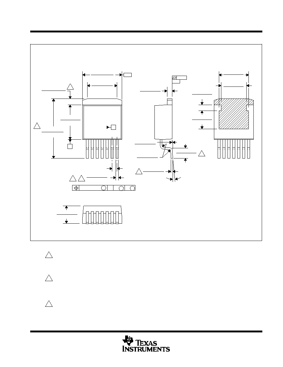
MPSF015 ≠ AUGUST 2001
POST OFFICE BOX 655303
∑
DALLAS, TEXAS 75265
KTW (R-PSFM-G7)
PLASTIC FLANGE-MOUNT
0.010 (0,25)
A
M
4201284/A 08/01
0.385 (9,78)
0.410 (10,41)
M
M
B
C
≠A≠
0.006
≠B≠
0.170 (4,32)
0.183 (4,65)
0.000 (0,00)
0.012 (0,305)
0.104 (2,64)
0.096 (2,44)
0.034 (0,86)
0.022 (0,57)
0.050 (1,27)
0.055 (1,40)
0.045 (1,14)
0.014 (0,36)
0.026 (0,66)
0.330 (8,38)
0.370 (9,40)
0.297 (7,54)
0.303 (7,70)
0.0585 (1,485)
0.0625 (1,587)
0.595 (15,11)
0.605 (15,37)
0.019 (0,48)
0.017 (0,43)
0
∞
~3
∞
0.179 (4,55)
0.187 (4,75)
0.056 (1,42)
0.064 (1,63)
0.296 (7,52)
0.304 (7,72)
0.300 (7,62)
0.252 (6,40)
F
C
C
H
H
H
C
A
NOTES: A. All linear dimensions are in inches (millimeters).
B. This drawing is subject to change without notice.
C. Lead width and height dimensions apply to the
plated lead.
D. Leads are not allowed above the Datum B.
E. Stand≠off height is measured from lead tip
with reference to Datum B.
F. Lead width dimension does not include dambar
protrusion. Allowable dambar protrusion shall not
cause the lead width to exceed the maximum
dimension by more than 0.003".
G. Cross≠hatch indicates exposed metal surface.
H. Falls within JEDEC MO≠169 with the exception
of the dimensions indicated.
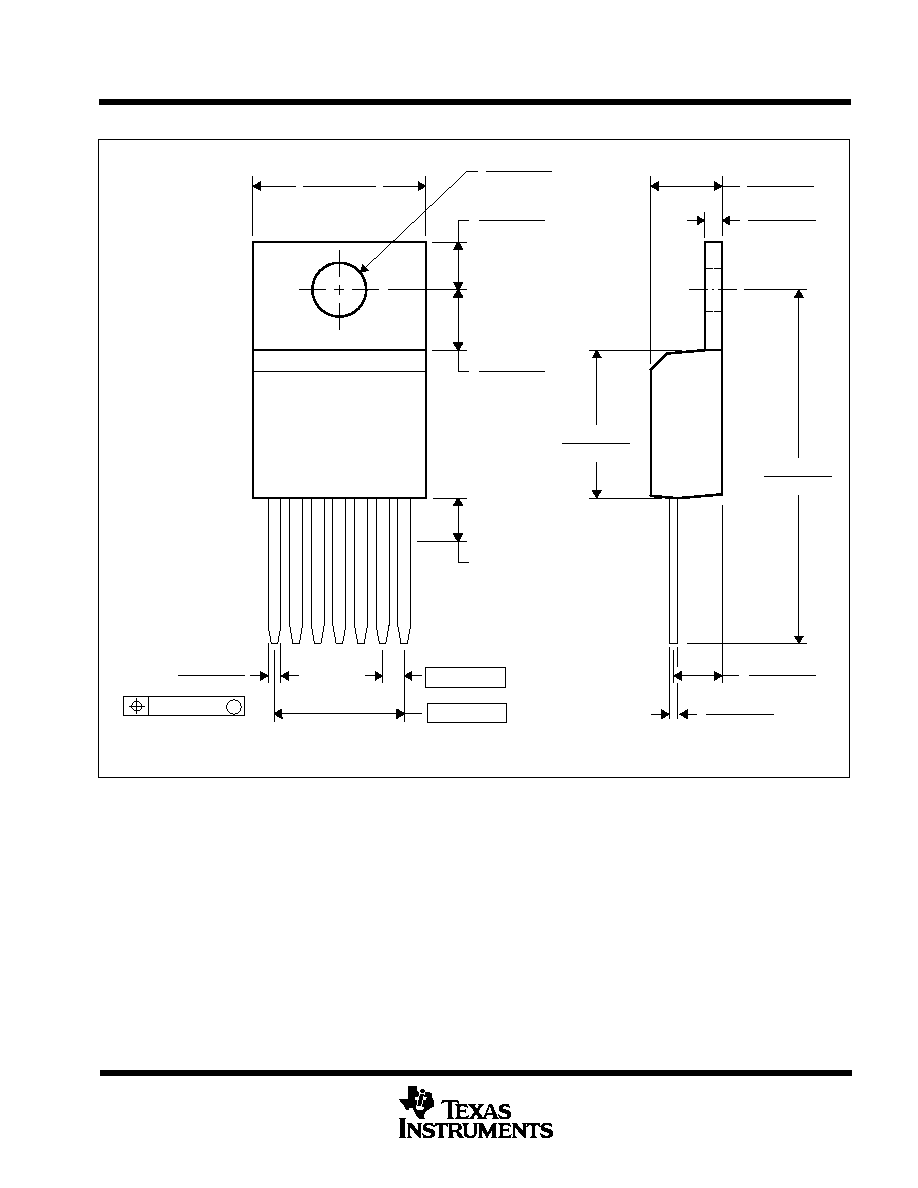
MECHANICAL DATA
MSOT010 ≠ OCTOBER 1994
1
POST OFFICE BOX 655303
∑
DALLAS, TEXAS 75265
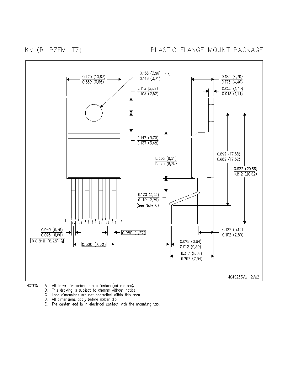
KC (R-PSFM-T7)
PLASTIC FLANGE-MOUNT PACKAGE
4040251 / B 01/95
0.420 (10,67)
0.055 (1,40)
0.335 (8,51)
0.030 (0,76)
0.026 (0,66)
0.380 (9,65)
0.325 (8,25)
0.045 (1,14)
0.113 (2,87)
0.103 (2,62)
0.146 (3,71)
0.156 (3,96)
0.122 (3,10)
0.102 (2,59)
DIA
(see Note C)
0.125 (3,18)
0.137 (3,48)
0.147 (3,73)
1.020 (25,91)
1.000 (25,40)
0.175 (4,46)
0.185 (4,70)
1
7
0.050 (1,27)
0.300 (7,62)
0.025 (0,64)
0.012 (0,30)
M
0.010 (0,25)
NOTES: A. All linear dimensions are in inches (millimeters).
B. This drawing is subject to change without notice.
C. Lead dimensions are not controlled within this area.
D. All lead dimensions apply before solder dip.
E. The center lead is in electrical contact with the mounting tab.

IMPORTANT NOTICE
Texas Instruments Incorporated and its subsidiaries (TI) reserve the right to make corrections, modifications,
enhancements, improvements, and other changes to its products and services at any time and to discontinue
any product or service without notice. Customers should obtain the latest relevant information before placing
orders and should verify that such information is current and complete. All products are sold subject to TI's terms
and conditions of sale supplied at the time of order acknowledgment.
TI warrants performance of its hardware products to the specifications applicable at the time of sale in
accordance with TI's standard warranty. Testing and other quality control techniques are used to the extent TI
deems necessary to support this warranty. Except where mandated by government requirements, testing of all
parameters of each product is not necessarily performed.
TI assumes no liability for applications assistance or customer product design. Customers are responsible for
their products and applications using TI components. To minimize the risks associated with customer products
and applications, customers should provide adequate design and operating safeguards.
TI does not warrant or represent that any license, either express or implied, is granted under any TI patent right,
copyright, mask work right, or other TI intellectual property right relating to any combination, machine, or process
in which TI products or services are used. Information published by TI regarding third-party products or services
does not constitute a license from TI to use such products or services or a warranty or endorsement thereof.
Use of such information may require a license from a third party under the patents or other intellectual property
of the third party, or a license from TI under the patents or other intellectual property of TI.
Reproduction of information in TI data books or data sheets is permissible only if reproduction is without
alteration and is accompanied by all associated warranties, conditions, limitations, and notices. Reproduction
of this information with alteration is an unfair and deceptive business practice. TI is not responsible or liable for
such altered documentation.
Resale of TI products or services with statements different from or beyond the parameters stated by TI for that
product or service voids all express and any implied warranties for the associated TI product or service and
is an unfair and deceptive business practice. TI is not responsible or liable for any such statements.
Following are URLs where you can obtain information on other Texas Instruments products and application
solutions:
Products
Applications
Amplifiers
amplifier.ti.com
Audio
www.ti.com/audio
Data Converters
dataconverter.ti.com
Automotive
www.ti.com/automotive
DSP
dsp.ti.com
Broadband
www.ti.com/broadband
Interface
interface.ti.com
Digital Control
www.ti.com/digitalcontrol
Logic
logic.ti.com
Military
www.ti.com/military
Power Mgmt
power.ti.com
Optical Networking
www.ti.com/opticalnetwork
Microcontrollers
microcontroller.ti.com
Security
www.ti.com/security
Telephony
www.ti.com/telephony
Video & Imaging
www.ti.com/video
Wireless
www.ti.com/wireless
Mailing Address:
Texas Instruments
Post Office Box 655303 Dallas, Texas 75265
Copyright
2003, Texas Instruments Incorporated